

Page 1
© 2000 Fairchild Semiconductor Corporation DS006433 www.fairchildsemi.com
August 1986
Revised March 2000
DM74LS390 Dual 4-Bit Decade Counter
DM74LS390
Dual 4-Bit Decade Counter
General Description
Each of these monolithic circuits contains eight masterslave flip-flops and additional gating to implement two individual four-bit counters in a single package. The
DM74LS390 incorporates dual divide-by-two and divideby-five counters, which can be used to implement cycle
lengths equal to any whole and/or cumulative multiples of 2
and/or 5 up to divi de-by- 100. Whe n c onnecte d as a bi-q uinary counter, the separate divide-by-two circuit can be
used to provide symmetry (a squ are wave ) at the final output stage. The DM74 LS39 0 ha s parallel outputs from ea ch
counter stage so that any submultiple of the input count frequency is available for system-timing signals.
Features
■ Dual version of the popular DM74LS90
■ DM74LS390...individual clocks for A and B flip-flops
provide dual ÷ 2 and ÷ 5 counters
■ Direct clear for each 4-bit counter
■ Dual 4-bit version can significa ntly impr ove syste m den-
sities by reducing counter package count by 50%
■ Typical maximum count frequency...35 MHz
■ Buffered outputs reduce possibility of collector commu-
tation
Ordering Code:
Devices also availab le in Tape and Reel. Specify by appending th e s uffix let t er “X” to the ordering code.
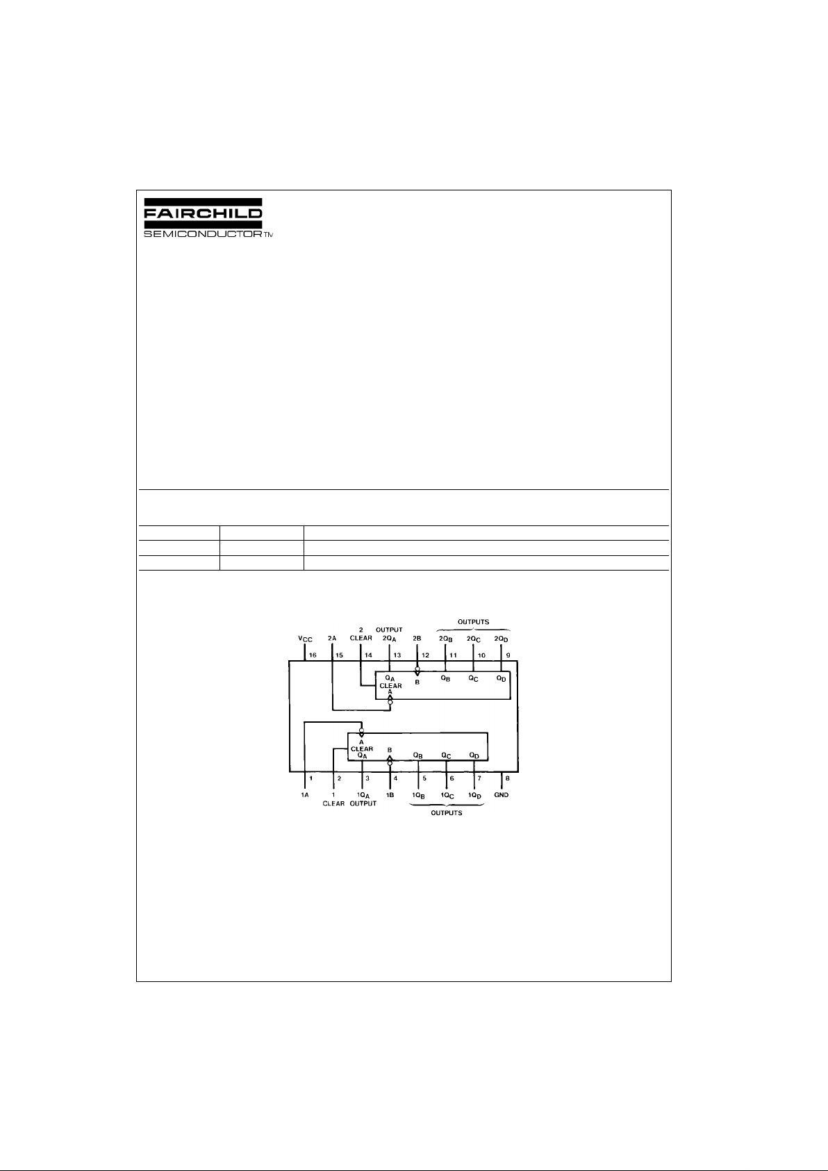
Connection Diagram
Order Number Package Number Package Description
DM74LS390M M16A 16-Lead Small Outline Integrated Circuit (SOIC), JEDEC MS-012, 0.150 Narrow
DM74LS390N N16E 16-Lead Plastic Dual-In-Line Package (PDIP), JEDEC MS-001, 0.300 Wide
Page 2
www.fairchildsemi.com 2
DM74LS390
Function Tables
BCD Count Sequence
(Each Counter) (Note 1)
Bi-Quinary (5-2)
(Each Counter) (Note 2)
H = HIGH Level
L = LOW Level
Note 1: Output Q
A
is connected to input B for BCD count.
Note 2: Output Q
D
is connected to input A for Bi-quinary count.
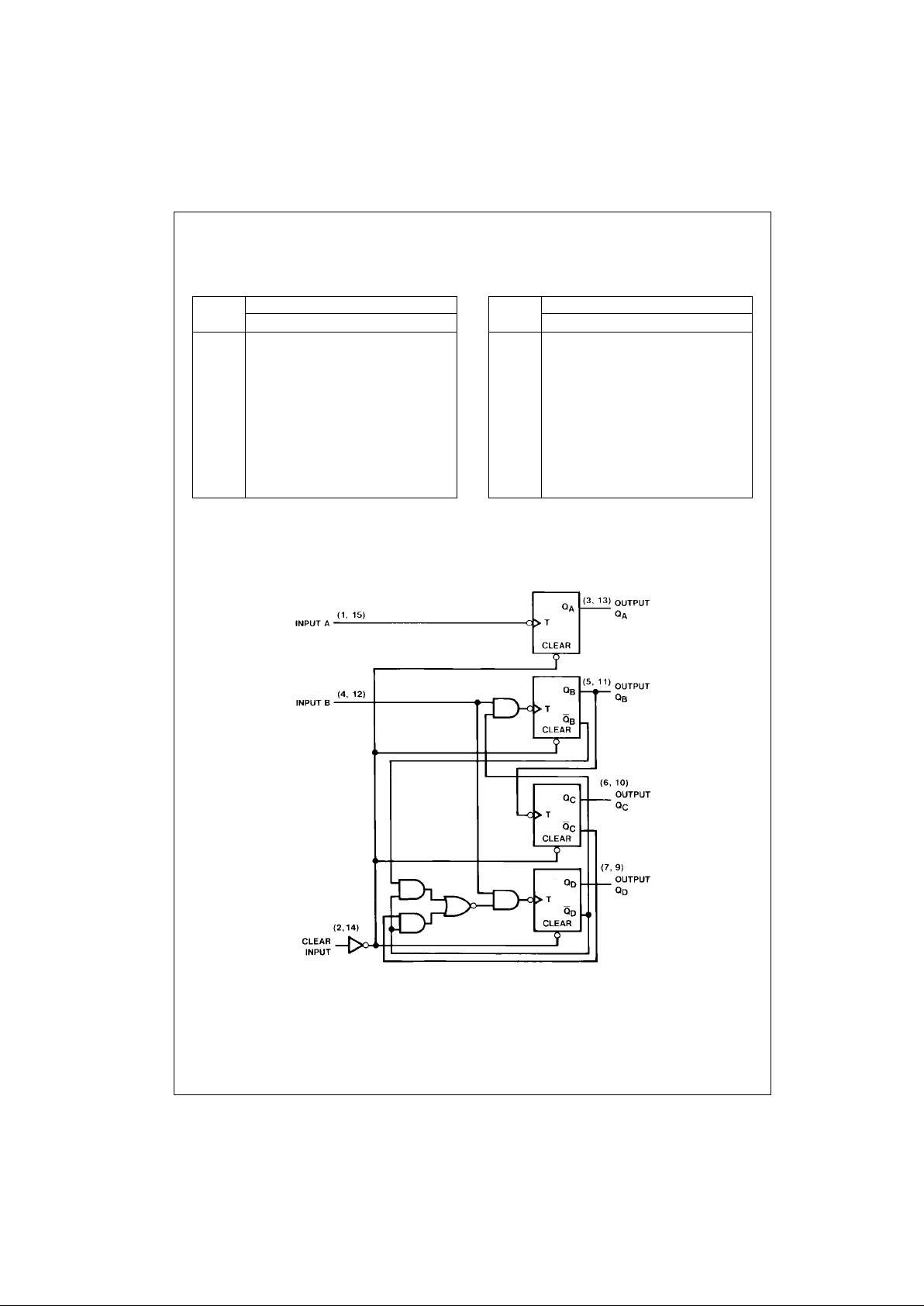
Logic Diagram
Count
Outputs
Q
D
Q
C
Q
B
Q
A
0LLLL
1LLLH
2LLHL
3LLHH
4LHLL
5LHLH
6LHHL
7LHHH
8HLLL
9HLLH
Count
Outputs
Q
A
Q
D
Q
C
Q
B
0LLLL
1LLLH
2LLHL
3LLHH
4LHLL
5HLLL
6HLLH
7HLHL
8HLHH
9HHLL
Page 3

3 www.fairchildsemi.com
DM74LS390
Absolute Maximum Ratings(Note 3)
Note 3: The “Absolute M aximu m R atin gs” are t hose valu es b eyo nd w hich
the safety of the device cannot be guaranteed. The device should not be
operated at these limits. The parametric values defined in the Electrical
Characteristics tables are not guaranteed at the absolute maximum ratings.
The “Recommend ed O peratin g Cond itions” t able w ill defin e the condition s
for actual device operation.
Recommended Operating Conditions
Note 4: CL = 15 pF, RL = 2 kΩ, TA = 25°C and VCC = 5V.
Note 5: C
L
= 50 pF, RL = 2 kΩ, TA = 25°C and VCC = 5V.
Note 6: The symbol (↓) indicates the falling edge of the clear pulse is used for reference.
Note 7: T
A
= 25°C and VCC = 5V.
Electrical Characteristics
over recommended operating free air temperature range (unless otherwise noted)
Note 8: All typicals are at VCC = 5V, TA = 25°C.
Note 9: Not more than one output should be shorted at a time, and the duration should not exceed one second.
Note 10: I
CC
is measured with all out put s OPEN, both CLEAR in puts grounded following momentary connec t ion to 4.5 and all other inp ut s grounded.
Supply Voltage 7V
Input Voltage
Clear 7V
A or B 5.5V
Operating Free Air Temperature Range 0°C to +70°C
Storage Temperature Range −65°C to +150°C
Symbol Parameter Min Nom Max Units
V
CC
Supply Voltage 4.75 5 5.25 V
V
IH
HIGH Level Input Voltage 2 V
V
IL
LOW Level Input Voltage 0.8 V
I
OH
HIGH Level Output Current −0.4 mA
I
OL
LOW Level Output Current 8 mA
f
CLK
Clock Frequency (Note 4) A to Q
A
025
MHz
B to Q
B
020
f
CLK
Clock Frequency (Note 5) A to Q
A
020
MHz
B to Q
B
015
t
W
Pulse Width (Note 4) A 20
B25 ns
Clear HIGH 20
t
REL
Clear Release Time (Note 6)(Note 7) 25↓ ns
T
A
Free Air Operating Temperature 0 70 °C
Symbol Parameter Conditions Min
Typ
Max Units
(Note 8)
V
I
Input Clamp Voltage VCC = Min, II = −18 mA −1.5 V
V
OH
HIGH Level VCC = Min, IOH = Max
2.7 3.4 V
Output Voltage VIL = Max, VIH = Min
V
OL
LOW Level VCC = Min, IOL = Max
0.35 0.5
Output Voltage VIL = Max, VIH = Min V
IOL = 4 mA, VCC = Min 0.25 0.4
I
I
Input Current @ Max VCC = Max, VI = 7V Clear 0.1
Input Voltage VCC = Max A 0.2 mA
VI = 5.5V B 0.4
I
IH
HIGH Level VCC = Max Clear 20
Input Current VI = 2.7V A 40 µA
B80
I
IL
LOW Level VCC = Max, VI = 0.4V Clear −0.4
Input Current A −1.6 mA
B −2.4
I
OS
Short Circuit Output Current VCC = Max (Note 9) −20 −100 mA
I
CC
Supply Current VCC = Max (Note 10) 15 26 mA
Page 4

www.fairchildsemi.com 4
DM74LS390
Switching Characteristics
at VCC = 5V and TA = 25°C
RL = 2 kΩ
Symbol Parameter From (Input)
CL = 15 pF CL = 50 pF
Units
To (Output) Min Max Min Max
f
MAX
Maximum Clock A to Q
A
25 20
MHz
Frequency B to Q
B
20 15
t
PLH
Propagation Delay Time
A to Q
A
20 24 ns
LOW-to-HIGH Level Output
t
PHL
Propagation Delay Time
A to Q
A
20 30 ns
HIGH-to-LOW Level Output
t
PLH
Propagation Delay Time
A to Q
C
60 81 ns
LOW-to-HIGH Level Output
t
PHL
Propagation Delay Time
A to Q
C
60 81 ns
HIGH-to-LOW Level Output
t
PLH
Propagation Delay Time
B to Q
B
21 27 ns
LOW-to-HIGH Level Output
t
PHL
Propagation Delay Time
B to Q
B
21 33 ns
HIGH-to-LOW Level Output
t
PLH
Propagation Delay Time
B to Q
C
39 51 ns
LOW-to-HIGH Level Output
t
PHL
Propagation Delay Time
B to Q
C
39 54 ns
HIGH-to-LOW Level Output
t
PLH
Propagation Delay Time
B to Q
D
21 27 ns
LOW-to-HIGH Level Output
t
PHL
Propagation Delay Time
B to Q
D
21 33 ns
HIGH-to-LOW Level Output
t
PHL
Propagation Delay Time
Clear to Any Q 39 45 ns
HIGH-to-LOW Level Output
Page 5

5 www.fairchildsemi.com
DM74LS390
Physical Dimensions inches (millimeters) unless otherwise noted
16-Lead Small Outline Integrated Circuit (SOIC), JEDEC MS-012, 0.150 Narrow
Package Number M16A
Page 6

6 www.fairchildsemi.com
DM74LS390 Dual 4-Bit Decade Counter
16-Lead Plastic Dual-In-Line Package (PDIP), JEDEC MS-001, 0.300 Wide
Package Number N16E
Fairchild does not assume any responsibility for use of any circu itry described, no circuit patent license s are implied and
Fairchild reserves the right at any time without notice to change said circuitry and specifications.
LIFE SUPPORT POLICY
FAIRCHILD’S PRODUCTS ARE NOT AUTHORIZED FOR USE AS CRITICAL COMPONENTS IN LIFE SUPPORT
DEVICES OR SYSTEMS WITHOUT THE EXPRESS WRITTEN APPROVAL OF THE PRESIDENT OF FAIRCHILD
SEMICONDUCTOR CORPORATION. As used herein:
1. Life support devices or systems are dev ic es or syste ms
which, (a) are intended for surgical implant into the
body, or (b) support or sustain life, and (c) whose failure
to perform when properly used in accordance with
instructions for use provided i n the labe li ng, can be re asonably expected to result in a significant injury to the
user.
2. A critical componen t in any com ponent o f a l ife supp ort
device or system whose failu re to perform can b e reasonably expected to c ause th e fa i lure of the li fe s upp or t
device or system, or to affect its safety or effectiveness.
www.fairchildsemi.com
 Loading...