

Datasheet DM74LS367AN, DM74LS367AMX, DM74LS367AM, DM74LS367ACW Datasheet (Fairchild Semiconductor)
Page 1
© 2000 Fairchild Semiconductor Corporation DS006429 www.fairchildsemi.com
August 1986
Revised March 2000
DM74LS367A Hex 3-STATE Buffer/Bus Driver
DM74LS367A
Hex 3-STATE Buffer/Bus Driver
General Description
This device contain s six independe nt gates eac h of which
performs a non-invertin g buffer function . The outpu ts have
the 3-STATE feature. Whe n enabled, the outputs exhibit
the low impedance characte ristics of a sta ndard LS outp ut
with additional drive capability to permit the driving of bus
lines without external r esistors. When disabled, both the
output transistors are turned OFF presenting a high-impedance state to the bus line. Thus the output will act n either
as a significant load n or as a d river. To minimize the possibility that two outputs will attempt to take a co mmon bus to
opposite logic levels, t he disable time is short er than the
enable time of the outputs.
Ordering Code:
Devices also availab le in Tape and Reel. Specify by appending th e s uffix let t er “X” to the ordering code.
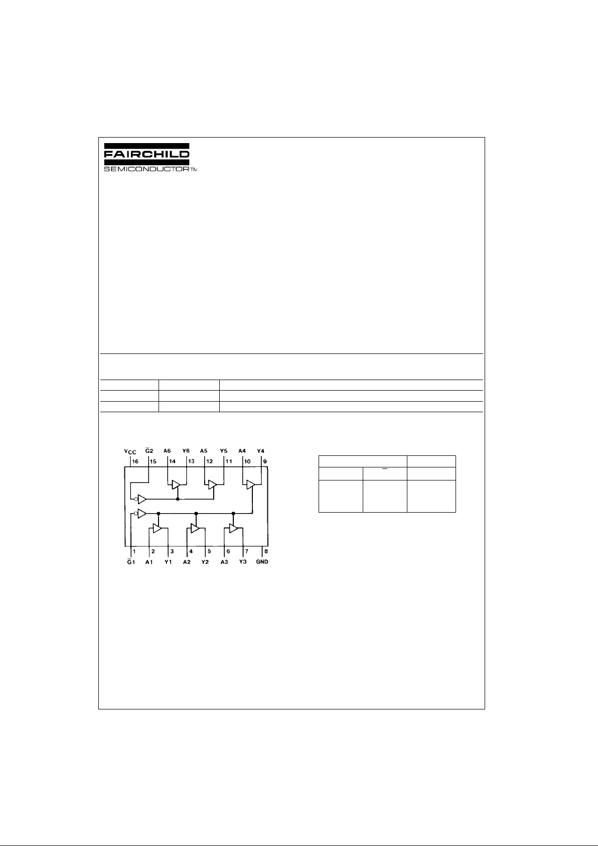
Connection Diagram Function Table
Y = A
H = HIGH Logic Level
L = LOW Logic Level
X = Either LOW or HIGH Logic Level
Hi-Z = 3-STATE (Outputs are disabled)
Order Number Package Number Package Description
DM74LS367AM M16A 16-Lead Small Outline Integrated Circuit (SOIC), JEDEC MS-012, 0.150 Narrow
DM74LS367AN N16E 16-Lead Plastic Dual-In-Line Package (PDIP), JEDEC MS-001, 0.300 Wide
Inputs Output
AG
Y
LL L
HL H
X H Hi-Z
Page 2
www.fairchildsemi.com 2
DM74LS367A
Absolute Maximum Ratings(Note 1)
Note 1: The “Absolute Maximum Ratin gs” are those v alues beyon d which
the safety of the dev ice cannot be guaranteed. T he device sh ould not be
operated at these limits. The parametric values defined in the Electrical
Characteristics tables are not guaranteed at the absolute maximum ratings.
The “Recommend ed O peratin g Cond itions” t able w ill defin e the co ndition s
for actual device operation.
Recommended Operating Conditions
Electrical Characteristics
over recommended operating free air temperature range (unless otherwise noted)
Note 2: All typicals are at VCC = 5V, TA = 25°C.
Note 3: Not more than one output should be shorted at a time, and the duration should not exceed one second.
Note 4: I
CC
is measured with the DATA inputs grounded and the OUTPUT CONTROLS at 4.5V.
Note 5: Both G
inputs are at 2V.
Note 6: Both G
inputs at 0.4V.
Switching Characteristics
at VCC = 5V and TA = 25°C
Note 7: CL = 5 pF.
Supply Voltage 7V
Input Voltage 7V
Operating Free Air Temperature Range 0°C to +70°C
Storage Temperature Range −65°C to +150°C
Symbol Parameter Min Nom Max Units
V
CC
Supply Voltage 4.75 5 5.25 V
V
IH
HIGH Level Input Voltage 2 V
V
IL
LOW Level Input Voltage 0.8 V
I
OH
HIGH Level Output Current −2.6 mA
I
OL
LOW Level Output Current 24 mA
T
A
Free Air Operating Temperature 0 70 °C
Symbol Parameter Conditions Min
Typ
Max Units
(Note 2)
V
I
Input Clamp Voltage VCC = Min, II = −18 mA −1.5 V
V
OH
HIGH Level VCC = Min, IOH = Max
2.4 3.4 V
Output Voltage VIL = Max, VIH = Min
V
OL
LOW Level VCC = Min, IOL = Max
0.35 0.5
Output Voltage VIL = Max, VIH = Min V
IOL = 12 mA, VCC = Min 0.25 0.4
I
I
Input Current @ Max Input Voltage VCC = Max, VI = 7V 0.1 mA
I
IH
HIGH Level Input Current VCC = Max, VI = 2.7V 20 µA
IIL LOW Level VCC = Max, VI = 0.5V (Note 5) A Input −20 µA
Input Current VCC = Max, VI = 0.4V (Note 6) A Input −0.4
mA
VCC = Max, VI = 0.4V G Input −0.4
I
OZH
Off-State Output Current with VCC = Max, VO = 2.4V
20 µA
HIGH Level Output Voltage Applied VIH = Min, VIL = Max
I
OZL
Off-State Output Current with VCC = Max, VO = 0.4V
−20 µA
LOW Level Output Voltage Applied VIH = Min, VIL = Max
I
OS
Short Circuit Output Current VCC = Max (Note 3) −20 −100 mA
I
CC
Supply Current VCC = Max (Note 4) 14 24 mA
RL = 667Ω
Symbol Parameter
CL = 50 pF CL = 150 pF
Units
Min Max Min Max
t
PLH
Propagation Delay Time LOW-to-HIGH Level Output 16 25 ns
t
PHL
Propagation Delay Time HIGH-to-LOW Level Output 16 25 ns
t
PZH
Output Enable Time to HIGH Level Output 30 40 ns
t
PZL
Output Enable Time to LOW Level Output 30 40 ns
t
PHZ
Output Disable Time from HIGH Level Output (Note 7) 20 ns
t
PLZ
Output Disable Time from LOW Level Output (Note 7) 20 ns
Page 3

3 www.fairchildsemi.com
DM74LS367A
Physical Dimensions inches (millimeters) unless otherwise noted
16-Lead Small Outline Integrated Circuit (SOIC), JEDEC MS-012, 0.150 Narrow
Package Number M16A
Page 4

www.fairchildsemi.com 4
DM74LS367A Hex 3-ST ATE Buffer/Bus Driver
Physical Dimensions inches (millimeters) unless otherwise noted (Continued)
16-Lead Plastic Dual-In-Line Package (PDIP), JEDEC MS-001, 0.300 Wide
Package Number N16E
Fairchild does not assume any responsibility for use of any circuitry described, no circuit pate nt licenses are implied and
Fairchild reserves the right at any time without notice to change said circuitry and specifications.
LIFE SUPPORT POLICY
FAIRCHILD’S PRODUCTS ARE NOT AUTHORIZED FOR USE AS CRITICAL COMPONENTS IN LIFE SUPPORT
DEVICES OR SYSTEMS WITHOUT THE EXPRESS WRITTEN APPROVAL OF THE PRESIDENT OF FAIRCHILD
SEMICONDUCTOR CORPORATION. As used herein:
1. Life support de vices o r syste ms are devices or syste ms
which, (a) are intended for surgical implant into the
body, or (b) support or sustain life, and (c) whose failure
to perform when properly used in accordance with
instructions for use provided in the labeling, can be reasonably expected to result in a significant inju ry to the
user.
2. A critical component in any com ponen t of a life su pport
device or system whose failu re to perform can be reasonably expected to ca use the fa i lure of the life su pp ort
device or system, or to affect its safety or effectiveness.
www.fairchildsemi.com
 Loading...