

Datasheet DM74LS283N, DM74LS283MX, DM74LS283M, DM74LS283CW Datasheet (Fairchild Semiconductor)
Page 1
© 2000 Fairchild Semiconductor Corporation DS006421 www.fairchildsemi.com
August 1986
Revised March 2000
DM74LS283 4-Bit Binary Adder with Fast Carry
DM74LS283
4-Bit Binary Adder with Fast Carry
General Description
These full adders perfor m the addition of two 4-bi t binary
numbers. The sum (∑) outputs are pr ovided for each bit
and the resultant car ry (C4 ) is obt aine d from the f ourth bit.
These adders feature full internal look ahead across all four
bits. This provides the system designer with partial lookahead performance at the econom y and red uced packa ge
count of a ripple-carry implementation.
The adder logic, i ncluding the carry, is implemente d in its
true form meaning that the end-around carry can be
accomplished without the need for logic or level inversion.
Features
■ Full-carry look-ahead across the four bits
■ Systems achieve partial look-ahead performance with
the economy of ripple carry
■ Typical add times
Two 8-bit words 25 ns
Two 1 6-bit words 45 ns
■ Typical power d issipation per 4-bit adder 95 mW
Ordering Code:
Devices also availab le in Tape and Reel. Specify by appending th e s uffix let t er “X” to the ordering code.
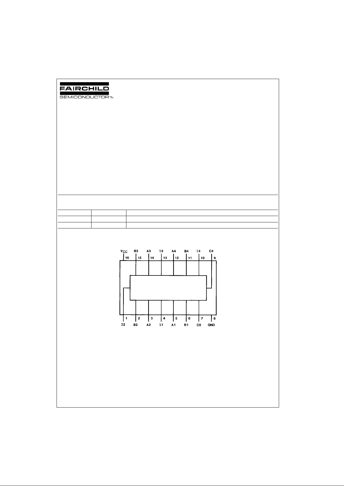
Connection Diagram
Order Number Package Number Package Description
DM74LS283M M16A 16-Lead Small Outline Integrated Circuit (SOIC), JEDEC MS-012, 0.150 Narrow
DM74LS283N N16E 16-Lead Plastic Dual-In-Line Package (PDIP), JEDEC MS-001, 0.300 Wide
Page 2
www.fairchildsemi.com 2
DM74LS283
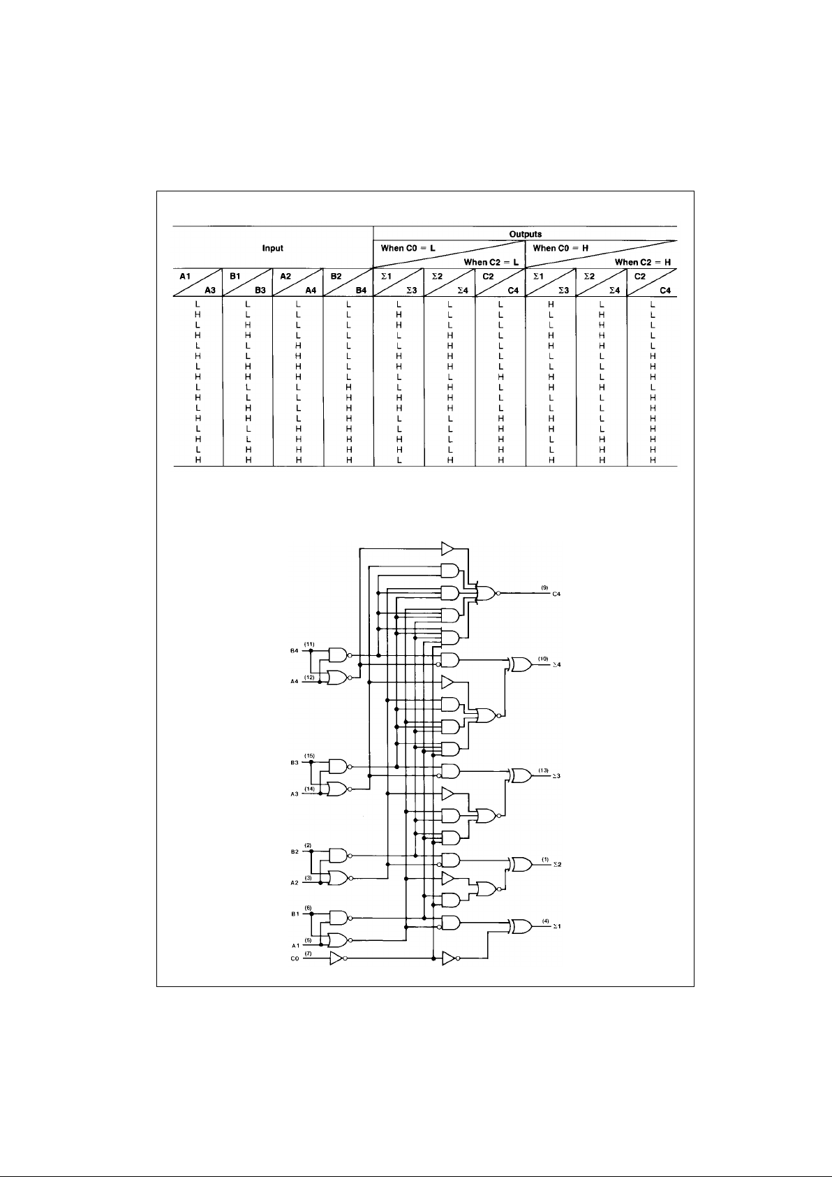
Function Table
H = HIGH Level, L = LOW Level
Input conditions at A1, B1, A2, B2, and C0 are us ed to determine outputs ∑1 and ∑2 and the value of the internal c arry C2.
The values at C2, A3 , B3, A4, and B4 are then use d to determine outputs ∑3, ∑4, and C4.
Logic Diagram
Page 3

3 www.fairchildsemi.com
DM74LS283
Absolute Maximum Ratings(Note 1)
Note 1: The “Absolute Maximum Ratings ” are those val ues beyond w hich
the safety of the device cannot be guaranteed. The device should not be
operated at these limits. The parametric values defined in the Electrical
Characteristics tables are not guaranteed at the absolute maximum ratings.
The “Recommend ed O peratin g Cond itions” t able w ill defin e the condition s
for actual device operation.
Recommended Operating Conditions
Electrical Characteristics
over recommended operating free air temperature range (unless otherwise noted)
Note 2: All typicals are at VCC = 5V, TA = 25°C.
Note 3: Not more than one output should be shorted at a time, and the duration should not exceed one second.
Note 4: I
CC1
is measured with all outputs OPEN, all B inp ut s LOW and all other inputs at 4. 5V, or all inputs at 4.5V.
Note 5: I
CC2
is measured with all outputs OPEN and all inputs GROUNDED.
Supply Voltage 7V
Input Voltage 7V
Operating Free Air Temperature Range 0°C to +70°C
Storage Temperature Range −65°C to +150°C
Symbol Parameter Min Nom Max Units
V
CC
Supply Voltage 4.75 5 5.25 V
V
IH
HIGH Level Input Voltage 2 V
V
IL
LOW Level Input Voltage 0.8 V
I
OH
HIGH Level Output Current −0.4 mA
I
OL
LOW Level Output Current 8 mA
T
A
Free Air Operating Tempe rature 0 70 °C
Symbol Parameter Conditions Min
Typ
Max Units
(Note 2)
V
I
Input Clamp Voltage VCC = Min, II = −18 mA −1.5 V
V
OH
HIGH Level VCC = Min, IOH = Max
2.7 3.4 V
Output Voltage VIL = Max, VIH = Min
V
OL
LOW Level VCC = Min, IOL = Max
0.35 0.5
Output Voltage VIL = Max, VIH = Min V
IOL = 4 mA, VCC = Min 0.25 0.4
I
I
Input Current @ Max VCC = Max A, B 0.2
mA
Input Voltage VI = 7V C0 0.1
I
IH
HIGH Level VCC = Max A, B 40
µA
Input Current VI = 2.7V C0 20
I
IL
LOW Level VCC = Max A, B −0.8
mA
Input Current VI = 0.4V C0 −0.4
I
OS
Short Circuit Output Current VCC = Max −20 −100 mA
I
CC1
Supply Current VCC = Max (Note 4) 19 34 mA
I
CC2
Supply Current VCC = Max (Note 5) 22 39 mA
Page 4

www.fairchildsemi.com 4
DM74LS283
Switching Characteristics
at VCC = 5V and TA = 25°C
From (Input) RL = 2 kΩ
Symbol Parameter
To (Output)
CL = 15 pF CL = 50 pF Units
MinMaxMinMax
t
PLH
Propagation Delay Time
C0 to ∑1, ∑22428ns
LOW-to-HIGH Level Output
t
PHL
Propagation Delay Time
C0 to ∑1, ∑22430ns
HIGH-to-LOW Level Output
t
PLH
Propagation Delay Time
C0 to ∑32428ns
LOW-to-HIGH Level Output
t
PHL
Propagation Delay Time
C0 to ∑32430ns
HIGH-to-LOW Level Output
t
PLH
Propagation Delay Time
C0 to ∑42428ns
LOW-to-HIGH Level Output
t
PHL
Propagation Delay Time
C0 to ∑42430ns
HIGH-to-LOW Level Output
t
PLH
Propagation Delay Time
Ai or Bi to ∑
i
24 28 ns
LOW-to-HIGH Level Output
t
PHL
Propagation Delay Time
Ai or Bi to ∑
i
24 30 ns
HIGH-to-LOW Level Output
t
PLH
Propagation Delay Time
C0 to C4 17 24 ns
LOW-to-HIGH Level Output
t
PHL
Propagation Delay Time
C0 to C4 17 25 ns
HIGH-to-LOW Level Output
t
PLH
Propagation Delay Time
Ai or Bi to C4 17 24 ns
LOW-to-HIGH Level Output
t
PHL
Propagation Delay Time
Ai or Bi to C4 17 26 ns
HIGH-to-LOW Level Output
Page 5

5 www.fairchildsemi.com
DM74LS283
Physical Dimensions inches (millimeters) unless otherwise noted
16-Lead Small Outline Integrated Circuit (SOIC), JEDEC MS-012, 0.150 Narrow
Package Number M16A
Page 6

www.fairchildsemi.com 6
DM74LS283 4-Bit Binary Adder with Fast Carry
Physical Dimensions inches (millimeters) unless otherwise noted (Continued)
16-Lead Plastic Dual-In-Line Package (PDIP), JEDEC MS-001, 0.300 Wide
Package Number N16E
Fairchild does not assume any responsibility for use of any circuitry described, no circuit pate nt licenses are implied and
Fairchild reserves the right at any time without notice to change said circuitry and specifications.
LIFE SUPPORT POLICY
FAIRCHILD’S PRODUCTS ARE NOT AUTHORIZED FOR USE AS CRITICAL COMPONENTS IN LIFE SUPPORT
DEVICES OR SYSTEMS WITHOUT THE EXPRESS WRITTEN APPROVAL OF THE PRESIDENT OF FAIRCHILD
SEMICONDUCTOR CORPORATION. As used herein:
1. Life support devices or systems are devices or syste ms
which, (a) are intended for surgical implant into the
body, or (b) support or sustain life, and (c) whose failure
to perform when properly used in accordance with
instructions for use provided in the labeling, can be reasonably expected to result in a significant inju ry to the
user.
2. A critical component i n any compon ent of a lif e support
device or system whose failu re to perform can be reasonably expected to ca use the fa i lure of the life su pp ort
device or system, or to affect its safety or effectiveness.
www.fairchildsemi.com
 Loading...