

Page 1
© 2000 Fairchild Semiconductor Corporation DS006420 www.fairchildsemi.com
August 1986
Revised March 2000
DM74LS279 Quad S-R Latch
DM74LS279
Quad S
-R Latch
General Description
The DM74LS279 consist s of four individual and indepe ndent Set-Reset Latches with active low inputs. Two of the
four latches have an add itiona l S
input ANDed with the pri-
mary S
input. A LOW on any S input while the R input is
HIGH will be stored in the latch and appear on the corresponding Q output as a HIGH. A LOW on the R
input while
the S
input is HIGH will clear the Q output to a LOW. Simul-
taneous transition of the R
and S inputs from LOW-toHIGH will cause the Q output to be indetermina te. Both
inputs are voltage leve l triggered and are no t affected by
transition time of the input data.
Ordering Code:
Devices also availab le in Tape and Reel. Specify by appending th e s uffix let t er “X” to the ordering code.
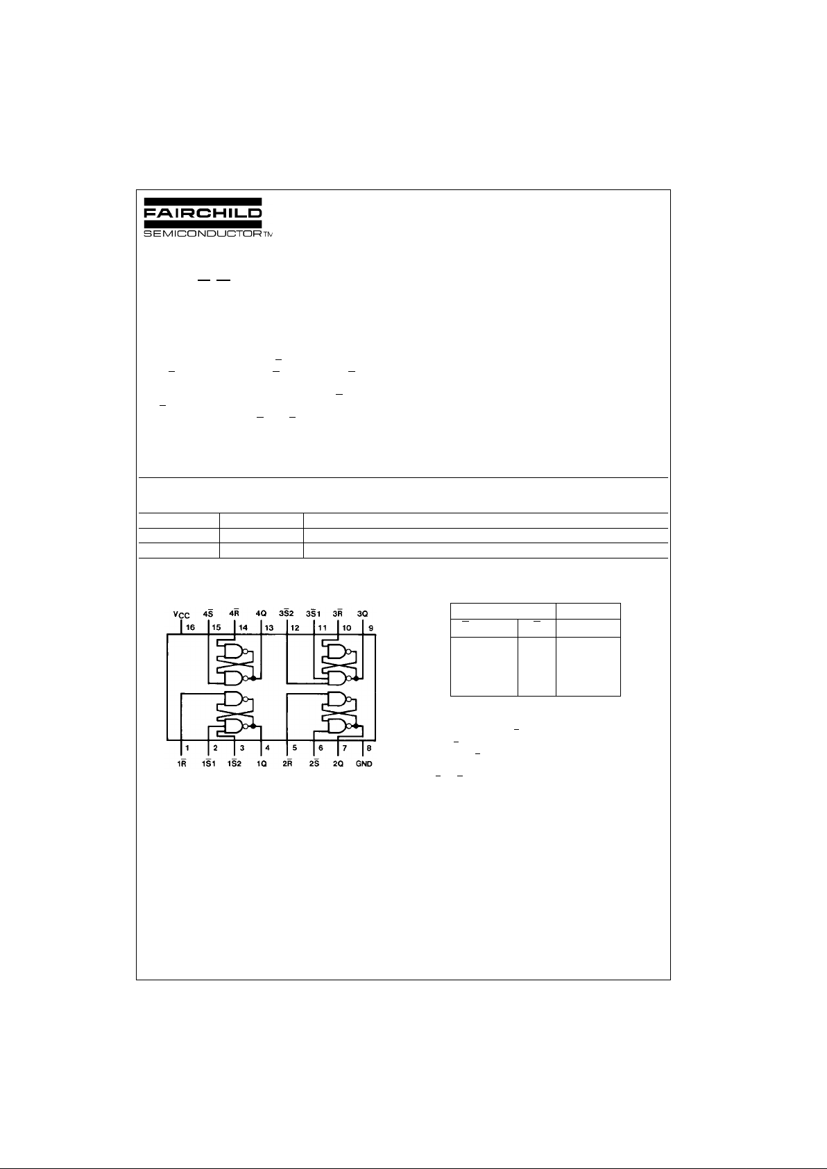
Connection Diagram Function Table
H = HIGH Level
L = LOW Level
Q0 = The Level of Q before the indica t ed input conditions were established.
Note 1: For latches with double S
inputs:
H = both S
inputs HIGH
L = one or both S
inputs LOW
Note 2: This output level is pse udo st able; that is, it may not per sist when
the S
and R inputs return to their inactive (HIGH) level.
Order Number Package Number Package Description
DM74LS279M M16A 16-Lead Small Outline Integrated Circuit (SOIC), JEDEC MS-012, 0.150 Narrow
DM74LS279N N16E 16-Lead Plastic Dual-In-Line Package (PDIP), JEDEC MS-001, 0.300 Wide
Inputs Output
S
(Note 1) R Q
L L H (Note 2)
LHH
HLL
HHQ
0
Page 2
www.fairchildsemi.com 2
DM74LS279
Absolute Maximum Ratings(Note 3)
Note 3: The “Absolute Maximum Ratin gs” are those v alues beyon d which
the safety of the dev ice cannot be guaranteed. T he device sh ould not be
operated at these limits. The parametric values defined in the Electrical
Characteristics tables are not guaranteed at the absolute maximum ratings.
The “Recommend ed O peratin g Cond itions” t able w ill defin e the co ndition s
for actual device operation.
Recommended Operating Conditions
Electrical Characteristics
over recommended operating free air temperature range (unless otherwise noted)
Note 4: All typicals are at VCC = 5V, TA = 25°C.
Note 5: Not more than one output should be shorted at a time, and the duration should not exceed one second.
Note 6: I
CC
is measured with all R in puts grounded, all S input s at 4. 5V and all outputs OPEN.
Switching Characteristics
at VCC = 5V and TA = 25°C
Supply Voltage 7V
Input Voltage 7V
Operating Free Air Temperature Range 0°C to +70°C
Storage Temperature Range −65°C to +150°C
Symbol Parameter Min Nom Max Units
V
CC
Supply Voltage 4.75 5 5.25 V
V
IH
HIGH Level Input Voltage 2 V
V
IL
LOW Level Input Voltage 0.8 V
I
OH
HIGH Level Output Current −0.4 mA
I
OL
LOW Level Output Current 8 mA
T
A
Free Air Operating Temperature 0 70 °C
Symbol Parameter Conditions Min
Typ
Max Units
(Note 4)
V
I
Input Clamp Voltage VCC = Min, II = −18 mA −1.5 V
V
OH
HIGH Level VCC = Min, IOH = Max
2.7 3.5 V
Output Voltage VIL = Max, VIH = Min
V
OL
LOW Level VCC = Min, IOL = Max
0.35 0.5
Output Voltage VIL = Max, VIH = Min V
IOL = 4 mA, VCC = Min 0.25 0.4
I
I
Input Current @ Max Input Voltage VCC = Max, VI = 7V 0.1 mA
I
IH
HIGH Level Input Current VCC = Max, VI = 2.7V 20 µA
I
IL
LOW Level Input Current VCC = Max, VI = 0.4V −0.4 mA
I
OS
Short Circuit Output Current VCC = Max (Note 5) −20 −100 mA
I
CC
Supply Current VCC = Max (Note 6) 3.8 7 mA
From (Input)
RL = 2 kΩ
Symbol Parameter
To (Output)
CL = 15 pF CL = 50 pF Units
Min Max Min Max
t
PLH
Propagation Delay Time
S to Q 22 25 ns
LOW-to-HIGH Level Output
t
PHL
Propagation Delay Time
S to Q 15 23 ns
HIGH-to-LOW Level Output
t
PHL
Propagation Delay Time
R to Q 27 33 ns
HIGH-to-LOW Level Output
Page 3

3 www.fairchildsemi.com
DM74LS279
Physical Dimensions inches (millimeters) unless otherwise noted
16-Lead Small Outline Integrated Circuit (SOIC), JEDEC MS-012, 0.150 Narrow
Package Number M16A
Page 4

www.fairchildsemi.com 4
DM74LS279 Quad S-R Latch
Physical Dimensions inches (millimeters) unless otherwise noted (Continued)
16-Lead Plastic Dual-In-Line Package (PDIP), JEDEC MS-001, 0.300 Wide
Package Number N16E
Fairchild does not assume any responsibility for use of any circuitry described, no circuit pate nt licenses are implied and
Fairchild reserves the right at any time without notice to change said circuitry and specifications.
LIFE SUPPORT POLICY
FAIRCHILD’S PRODUCTS ARE NOT AUTHORIZED FOR USE AS CRITICAL COMPONENTS IN LIFE SUPPORT
DEVICES OR SYSTEMS WITHOUT THE EXPRESS WRITTEN APPROVAL OF THE PRESIDENT OF FAIRCHILD
SEMICONDUCTOR CORPORATION. As used herein:
1. Life support devices or systems are devices or syste ms
which, (a) are intended for surgical implant into the
body, or (b) support or sustain life, and (c) whose failure
to perform when properly used in accordance with
instructions for use provided in the labeling, can be reasonably expected to result in a significant inju ry to the
user.
2. A critical component i n any compon ent of a lif e support
device or system whose failu re to perform can be reasonably expected to ca use the fa i lure of the life su pp ort
device or system, or to affect its safety or effectiveness.
www.fairchildsemi.com
 Loading...