

Datasheet DM74LS259WM, DM74LS259N, DM74LS259MX, DM74LS259M, DM74LS259CW Datasheet (Fairchild Semiconductor)
...Page 1
© 2000 Fairchild Semiconductor Corporation DS006418 www.fairchildsemi.com
August 1986
Revised March 2000
DM74LS259 8-Bit Addressable Latches
DM74LS259
8-Bit Addressable Latches
General Description
These 8-bit addressable latche s are designed for general
purpose storage applications in digital systems. Specific
uses include working registers, serial-holding registers,
and active-high de coders or de mult iplexers. Th ey are multifunctional devices capable of storing single-line data in
eight addressable latch es, and being a 1-of-8 decoder or
demultiplexer with active-high outputs.
Four distinct modes of ope ration are select able b y contr olling the clear and enable inputs as enumerated in the function table. In the addre ssab le-l a tch mod e, d ata at the dat ain terminal is written into the addressed latch. The
addressed latch will follow the data input with all unaddressed latches remaining in th eir previous states. In the
memory mode, all latches rem ain in their previous states
and are unaffected by the data o r addre ss inputs. To eliminate the possibility of entering erroneous data in the
latches, the enable should be held HIGH (inactive) while
the address lines are changing. In the 1-of-8 decoding or
demultiplexing mode, the addressed o utput will follow the
level of the D input with all other o utputs LO W. In the clear
mode, all outputs are LO W and un affected by the addr ess
and data inputs.
Features
■ 8-Bit parallel-out stora ge register pe rforms ser ial-to-parallel conversion with storage
■ Asynchronous parallel clear
■ Active high decoder
■ Enable/disable input simplifies expansion
■ Direct replacement for Fairchild DM9334
■ Expandable for N-bit applic atio ns
■ Four distinct functional modes
■ Typical propagation delay times:
Enable-to-output 18 ns
Data-to-output 16 ns
Address-to-output 21 ns
Clear-to-output 17 ns
■ Fan-out
I
OL
(sink current) 8 mA
I
OH
(source current) −0.4 mA
■ Typical I
CC
22 mA
Ordering Code:
Devices also availab le in Tape and Reel. Specify by appending th e s uffix let t er “X” to the ordering code.
Order Number Package Number Package Description
DM74LS259M M16A 16-Lead Small Outlin e Integrated Circuit (SOIC), JEDEC MS-012, 0.150 Narrow
DM74LS259WM M16B 16-Lead Small Outline Intergrated Circuit (SOIC), JEDEC MS-013, 0.300 Wide
DM74LS259N N16E 16-Lead Plastic Dual-In-Line Package (PDIP), JEDEC MS-001, 0.300 Wide
Page 2
www.fairchildsemi.com 2
DM74LS259
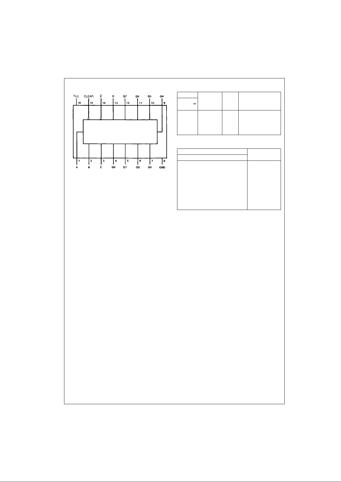
Connection Diagram Function Table
Latch Selection Table
H = HIGH Level
L = LOW Level
D = the Level of the Data Input
Q
i0
= the Level of Qi (i = 0, 1,…7, as A ppropriate) before the Indicated
Steady-State Input Conditions Were Est ablished.
Inputs Output of Each
Addressed Other Function
Clear E
Latch Output
HL D Q
i0
Addressable Latch
HH Q
i0
Qi0Memory
L L D L 8-Line Demultiplexer
L H L L Clear
Select Inputs Latch
C B A Addressed
LLL 0
LLH 1
LHL 2
LHH 3
HLL 4
HLH 5
HHL 6
HHH 7
Page 3

3 www.fairchildsemi.com
DM74LS259
Absolute Maximum Ratings(Note 1)
Note 1: The “Absolute Maximum Ratings ” are those val ues beyond w hich
the safety of the device cannot be guaranteed. The device should not be
operated at thes e limits. The paramet ric values defined in the “Electrical
Characteristics” ta ble are not guaranteed at the absolute maxim um ratings.
The “Recommend ed O peratin g Cond itions” t able w ill defin e the condition s
for actual device operation.
Recommended Operating Conditions
Note 2: The symbols (↓, ↑) indicate the edge of th e c loc k pulse used for referenc e: ↑ for rising ed ge, ↓ for falling edge.
Note 3: Setup and hold t im es are with reference to the enable input.
Note 4: The select-to-enab le setup time is the tim e before the HIGH- to-LOW enable tr ansition that the sele ct must be stable so that the correct latch is
selected and the others not affected.
Note 5: T
A
= 25°C and VCC = 5V.
Electrical Characteristics
over recommended operating free air temperature range (unless otherwise noted)
Note 6: All typicals are at VCC = 5V, TA = 25°C.
Note 7: Not more than one output should be shorted at a time, and the duration should not exceed one second.
Note 8: I
CC
is measured with all inputs at 4.5V, and all outputs OPEN.
Supply Voltage 7V
Input Voltage 7V
Operating Free Air Temperature Range 0°C to +70°C
Storage Temperature Range −65°C to +150°C
Symbol Parameter Min Nom Max Units
V
CC
Supply Voltage 4.75 5 5.25 V
V
IH
HIGH Level Input Voltage 2 V
V
IL
LOW Level Input Voltage 0.8 V
I
OH
HIGH Level Output Current −0.4 mA
I
OL
LOW Level Output Current 8 mA
t
W
Pulse Width Enable 15
ns
(Note 5) Clear 15
t
SU
Setup Time Data 15↑
ns
(Note 2)(Note 3)(Note 4)(Note 5) Select 15↓
t
H
Hold Time Data 2.5↑
ns
(Note 2)(Note 3)(Note 5) Select 2.5↑
T
A
Free Air Operating Temperature 0 70 °C
Symbol Parameter Conditions Min
Typ
Max Units
(Note 6)
V
I
Input Clamp Voltage VCC = Min, II = −18 mA −1.5 V
V
OH
HIGH Level VCC = Min, IOH = Max
2.7 3.4 V
Output Voltage VIL = Max, VIH = Min
V
OL
LOW Level VCC = Min, IOL = Max
0.35 0.5
Output Voltage VIL = Max, VIH = Min V
IOL = 4 mA, VCC = Min 0.25 0.4
I
I
Input Current @ Max VCC = Max, VI = 7V
0.1 mA
Input Voltage VI = 10V
I
IH
HIGH Level Input Current VCC = Max, VI = 2.7V 20 µA
I
IL
LOW Level Input Current VCC = Max, VI = 0.4V −0.4
mA
Enable VCC = Max, VI = 0.4V −0.8
I
OS
Short Circuit Output Current VCC = Max (Note 7) −20 −100 mA
I
CC
Supply Current VCC = Max (Note 8) 22 36 mA
Page 4

www.fairchildsemi.com 4
DM74LS259
Switching Characteristics
at VCC = 5V and TA = 25°C
Symbol Parameter
From (Input) CL = 50 pF
UnitsTo (Output) RL = 2 kΩ
Min Max
t
PLH
Propagation Delay Time
Enable to Output 38 ns
LOW-to-HIGH Level Output
t
PHL
Propagation Delay Time
Enable to Output 32 ns
HIGH-to-LOW Level Output
t
PLH
Propagation Delay Time
Data to Output 35 ns
LOW-to-HIGH Level Output
t
PHL
Propagation Delay Time
Data to Output 30 ns
HIGH-to-LOW Level Output
t
PLH
Propagation Delay Time
Select to Output 41 ns
LOW-to-HIGH Level Output
t
PHL
Propagation Delay Time
Select to Output 38 ns
HIGH-to-LOW Level Output
t
PHL
Propagation Delay Time
Clear to Output 36 ns
HIGH-to-LOW Level Output
Page 5

5 www.fairchildsemi.com
DM74LS259
Physical Dimensions inches (millimeters) unless otherwise noted
16-Lead Small Outline Integrated Circuit (SOIC), JEDEC MS-012, 0.150 Narrow
Package Number M16A
16-Lead Small Outline Intergrated Circuit (SOIC), JEDEC MS-013, 0.300 Wide
Package Number M16B
Page 6

www.fairchildsemi.com 6
DM74LS259 8-Bit Addressable Latches
Physical Dimensions inches (millimeters) unless otherwise noted (Continued)
16-Lead Plastic Dual-In-Line Package (PDIP), JEDEC MS-001, 0.300 Wide
Package Number N16E
Fairchild does not assume any responsibility for use of any circuitry described, no circuit pate nt licenses are implied and
Fairchild reserves the right at any time without notice to change said circuitry and specifications.
LIFE SUPPORT POLICY
FAIRCHILD’S PRODUCTS ARE NOT AUTHORIZED FOR USE AS CRITICAL COMPONENTS IN LIFE SUPPORT
DEVICES OR SYSTEMS WITHOUT THE EXPRESS WRITTEN APPROVAL OF THE PRESIDENT OF FAIRCHILD
SEMICONDUCTOR CORPORATION. As used herein:
1. Life support devices or systems are devices or syste ms
which, (a) are intended for surgical implant into the
body, or (b) support or sustain life, and (c) whose failure
to perform when properly used in accordance with
instructions for use provided in the labeling, can be reasonably expected to result in a significant inju ry to the
user.
2. A critical component i n any compon ent of a lif e support
device or system whose failu re to perform can be reasonably expected to ca use the fa i lure of the life su pp ort
device or system, or to affect its safety or effectiveness.
www.fairchildsemi.com
 Loading...