

Page 1
© 2000 Fairchild Semiconductor Corporation DS006416 www.fairchildsemi.com
August 1986
Revised March 2000
DM74LS253 3-STATE Data Selector/Multiplexer
DM74LS253
3-STATE Data Selector/Multiplexer
General Description
Each of these Schottky-clamped data selector s/multiplexers contains inverter s and drivers to supply ful ly complementary, on-chip, binary decoding data selection to the
AND-OR gates. Separate output control inputs are provided for each of the two four-line sections.
The 3-STATE outputs can interface di rectly with data l ines
of bus-organized syste ms. Wit h all but one of the co mmon
outputs disabled (at a high impedance state), the low
impedance of the single enabled output will drive the bus
line to a HIGH or LOW logic level.
Features
■ 3-STATE version of DM74LS153 with same pinout
■ Schottky-diode-clamp ed tra nsisto rs
■ Permit multiplexing from N-lines to one line
■ Performs parallel-to-serial con version
■ Strobe/output control
■ High fanout totem-pole outputs
■ Typical propagation delay
Data to output 12 ns
Select to output 21 ns
■ Typical power di ssipation 35 mW
Ordering Code:
Devices also availab le in Tape and Reel. Specify by appending th e s uffix let t er “X” to the ordering code.
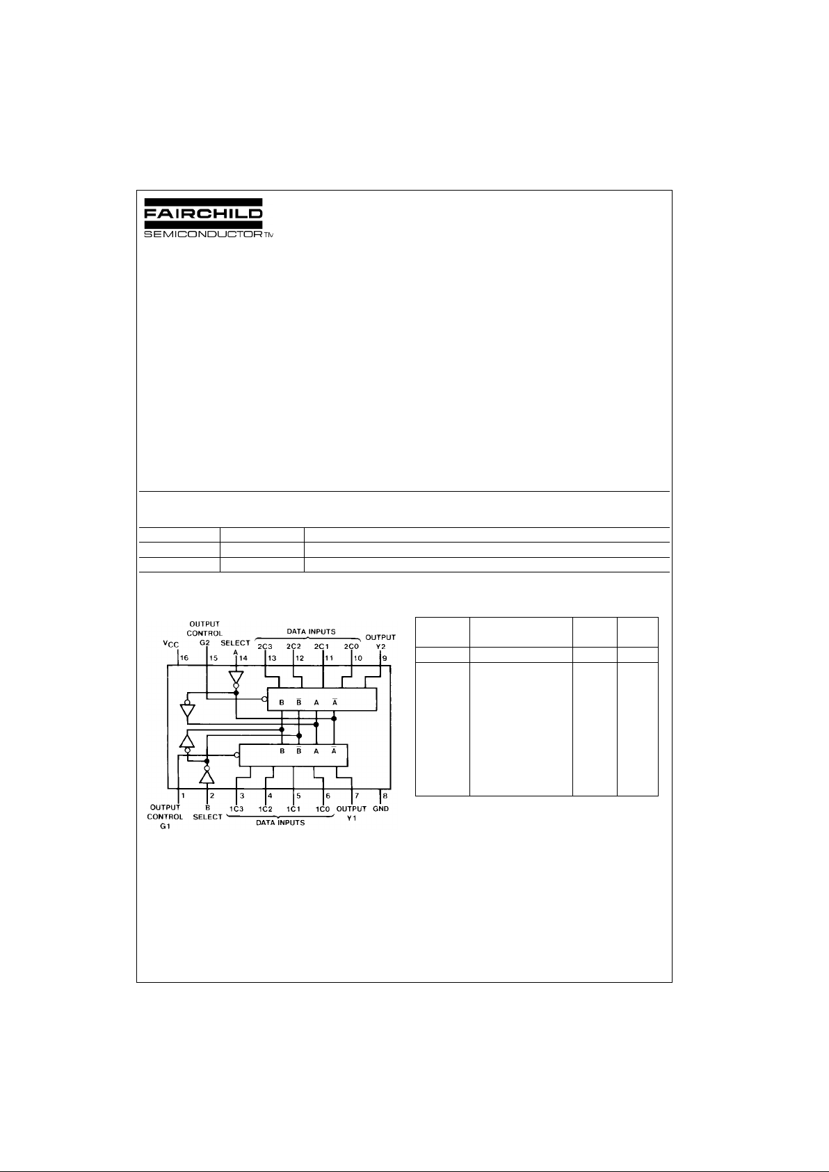
Connection Diagram Function Table
Address Inputs A and B are common to both sections.
H = HIGH Level
L = LOW Level
X = Don't Care
Z = High Impedance (OF F )
Order Number Package Number Package Description
DM74LS253M M16A 16-Lead Small Outline Integrated Circuit (SOIC), JEDEC MS-0 12, 0.150 Narrow
DM74LS253N N16E 16-Lead Plastic Dual-In-Line Package (PDIP), JEDEC MS-001, 0.300 Wide
Select Data Inputs Output Output
Inputs Control
B A C0 C1 C2 C3 G Y
XXXXXX H Z
LLLXXX L L
LLHXXX L H
LHXLXX L L
LHXHXX L H
HLXXLX L L
HLXXHX L H
HHXXXL L L
HHXXXH L H
Page 2
www.fairchildsemi.com 2
DM74LS253
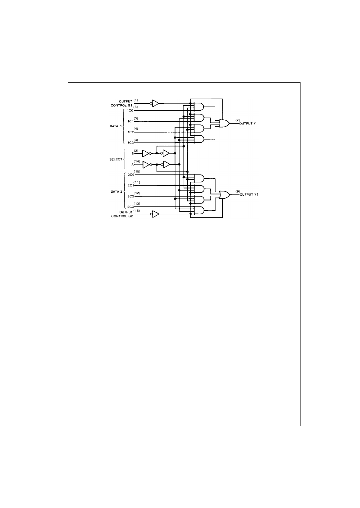
Logic Diagram
Page 3

3 www.fairchildsemi.com
DM74LS253
Absolute Maximum Ratings(Note 1)
Note 1: The “Absolute M aximu m R atin gs” are t hose valu es b eyo nd w hich
the safety of the device cannot be guaranteed. The device should not be
operated at thes e limits. The paramet ric values defined in the “Electrical
Characteristics” ta ble are not guaranteed at the absolute maxim um ratings.
The “Recommend ed O peratin g Cond itions” t able w ill defin e the condition s
for actual device operation.
Recommended Operating Conditions
Electrical Characteristics
over recommended operating free air temperature range (unless otherwise noted)
Note 2: All typicals are at VCC = 5V, TA = 25°C.
Note 3: Not more than one output should be shorted at a time, and the duration should not exceed one second.
Note 4: I
CC1
is measured with all outputs OPEN, and al l th e inputs grounded.
Note 5: I
CC2
is measured with the outputs OPEN, OUTPUT CONTROL at 4.5V and all other inputs grounded.
Supply Voltage 7V
Input Voltage 7V
Operating Free Air Temperature Range 0°C to +70°C
Storage Temperature Range −65°C to +150°C
Symbol Parameter Min Nom Max Units
V
CC
Supply Voltage 4.75 5 5.25 V
V
IH
HIGH Level Input Voltage 2 V
V
IL
LOW Level Input Voltage 0.8 V
I
OH
HIGH Level Output Current −2.6 mA
I
OL
LOW Level Output Current 24 mA
T
A
Free Air Operating Temperature 0 70 °C
Symbol Parameter Conditions Min
Typ
Max Units
(Note 2)
V
I
Input Clamp Voltage VCC = Min, II = −18 mA −1.5 V
V
OH
HIGH Level VCC = Min, IOH = Max
2.4 3.1 V
Output Voltage VIL = Max, VIH = Min
V
OL
LOW Level VCC = Min, IOL = Max
0.5
Output Voltage VIL = Max, VIH = Min V
IOL = 12 mA, VCC = Min 0.4
I
I
Input Current @ Max Input Voltage VCC = Max, VI = 7V 0.1 mA
I
IH
HIGH Level Input Current VCC = Max, VI = 2.7V 20 µA
I
IL
LOW Level Input Current VCC = Max, VI = 0.4V −0.4 mA
I
OZH
Off-State Output Current with VCC = Max, VO = 2.7V
20 µA
HIGH Level Output Voltage Applied VIH = Min, VIL = Max
I
OZL
Off-State Output Current with VCC = Max, VO = 0.4
−20 µA
LOW Level Output Voltage Applied VIH = Min, VIL = Max
I
OS
Short Circuit Output Current VCC = Max (Note 3) −20 −100 mA
I
CC1
Supply Current VCC = Max (Note 4) 7 12 mA
I
CC2
Supply Current VCC = Max (Note 5) 8.5 14 mA
Page 4

www.fairchildsemi.com 4
DM74LS253
Switching Characteristics
at VCC = 5V and TA = 25°C
Note 6: CL = 5 pF.
From (Input)
RL = 667Ω
Symbol Parameter
To (Output)
CL = 45 pF CL = 150 pF Units
MinMaxMinMax
t
PLH
Propagation Delay Time
Data to Y 25 35 ns
LOW-to-HIGH Level Output
t
PHL
Propagation Delay Time
Data to Y 20 30 ns
HIGH-to-LOW Level Output
t
PLH
Propagation Delay Time
Select to Y 45 54 ns
LOW-to-HIGH Level Output
t
PHL
Propagation Delay Time
Select to Y 32 44 ns
HIGH-to-LOW Level Output
t
PZH
Output Enable Time to Output
18 32 ns
HIGH Level Output Control to Y
t
PZL
Output Enable Time to Output
23 35 ns
LOW Level Output Control to Y
t
PHZ
Output Disable Time from Output
41 ns
HIGH Level Output (Note 6) Control to Y
t
PLZ
Output Disable Time from Output
27 ns
LOW Level Output (Note 6) Control to Y
Page 5

5 www.fairchildsemi.com
DM74LS253
Physical Dimensions inches (millimeters) unless otherwise noted
16-Lead Small Outline Integrated Circuit (SOIC), JEDEC MS-012, 0.150 Narrow
Package Number M16A
Page 6

www.fairchildsemi.com 6
DM74LS253 3-STATE Data Selector/Multiplexer
Physical Dimensions inches (millimeters) unless otherwise noted (Continued)
16-Lead Plastic Dual-In-Line Package (PDIP), JEDEC MS-001, 0.300 Wide
Package Number N16E
Fairchild does not assume any responsibility for use of any circuitry described, no circuit pate nt licenses are implied and
Fairchild reserves the right at any time without notice to change said circuitry and specifications.
LIFE SUPPORT POLICY
FAIRCHILD’S PRODUCTS ARE NOT AUTHORIZED FOR USE AS CRITICAL COMPONENTS IN LIFE SUPPORT
DEVICES OR SYSTEMS WITHOUT THE EXPRESS WRITTEN APPROVAL OF THE PRESIDENT OF FAIRCHILD
SEMICONDUCTOR CORPORATION. As used herein:
1. Life support devices or systems are device s or syste ms
which, (a) are intended for surgical implant into the
body, or (b) support or sustain life, and (c) whose failure
to perform when properly used in accordance with
instructions for use provided in the labeling, can be reasonably expected to result in a significant inju ry to the
user.
2. A critic al com ponent in any compon ent of a l ife supp ort
device or system whose failu re to perform can be reasonably expected to ca use the fa i lure of the life su pp ort
device or system, or to affect its safety or effectiveness.
www.fairchildsemi.com
 Loading...