

Datasheet DM74LS251N, DM74LS251MX, DM74LS251M, DM74LS251CW Datasheet (Fairchild Semiconductor)
Page 1

© 2000 Fairchild Semiconductor Corporation DS006415 www.fairchildsemi.com
August 1986
Revised March 2000
DM74LS251 3-STATE 1-of-8 Line Data Selector/Multiplexer
DM74LS251
3-STATE 1-of-8 Line Data Selector/Multiplexer
General Description
These data selectors/multiplexers contain full on-chip
binary decoding to select one-o f-eight data sources, and
feature a strobe-controlled 3-STATE output. The strobe
must be at a low logic level to enable these devices. The 3STATE outputs permit direct connection to a common bus.
When the strobe input is HIGH , both out put s are in a hig himpedance state in which both the upper and lower transistors of each totem-pole output are OFF, and the output neither drives nor loads the bus significantly. When the strobe
is LOW, the outputs are activa ted a nd op era te as standard
TTL totem-pole outputs.
To minimize the possibility that two outputs will attempt to
take a common bus to opposite logic levels, the output control circuitry is designed so th at the ave rage ou tput disa ble
time is shorter than the average output enable time.
Features
■ 3-STATE version of DM74LS151
■ Interface directly with system bus
■ Perform parallel-to-serial conversion
■ Permit multiplexing from N-lines to one line
■ Complementary outputs provide true and inverted data
■ Maximum number of common outputs: 129
■ Typical propagation delay time (D to Y): 17 ns
■ Typical power dissipation: 35 mW
Ordering Code:
Devices also availab le in Tape and Reel. Specify by appending th e s uffix let t er “X” to the ordering code.
Connection Diagram Function Table
H = HIGH Logic Level
L = LOW Logic Level
X = Don't Care
Z = High Impedance (OF F )
D0, D1…D7 = The level of the respe ctiv e D input
Order Number Package Number Package Description
DM74LS251M M16A 16-Lead Small Outline Integrated Circuit (SOIC), JED EC MS-012, 0.150 Narrow
DM74LS251N N16E 16-Lead Plastic Dual-In-Line Package (PDIP), JEDEC MS-001, 0.300 Wide
Inputs Outputs
Select Strobe
YW
CBA S
XXX H Z Z
LLL L D0D0
LLH L D1D1
LHL L D2D2
LHH L D3D3
HLL L D4D4
HLH L D5D5
HHL L D6D6
HHH L D7D7
Page 2
www.fairchildsemi.com 2
DM74LS251
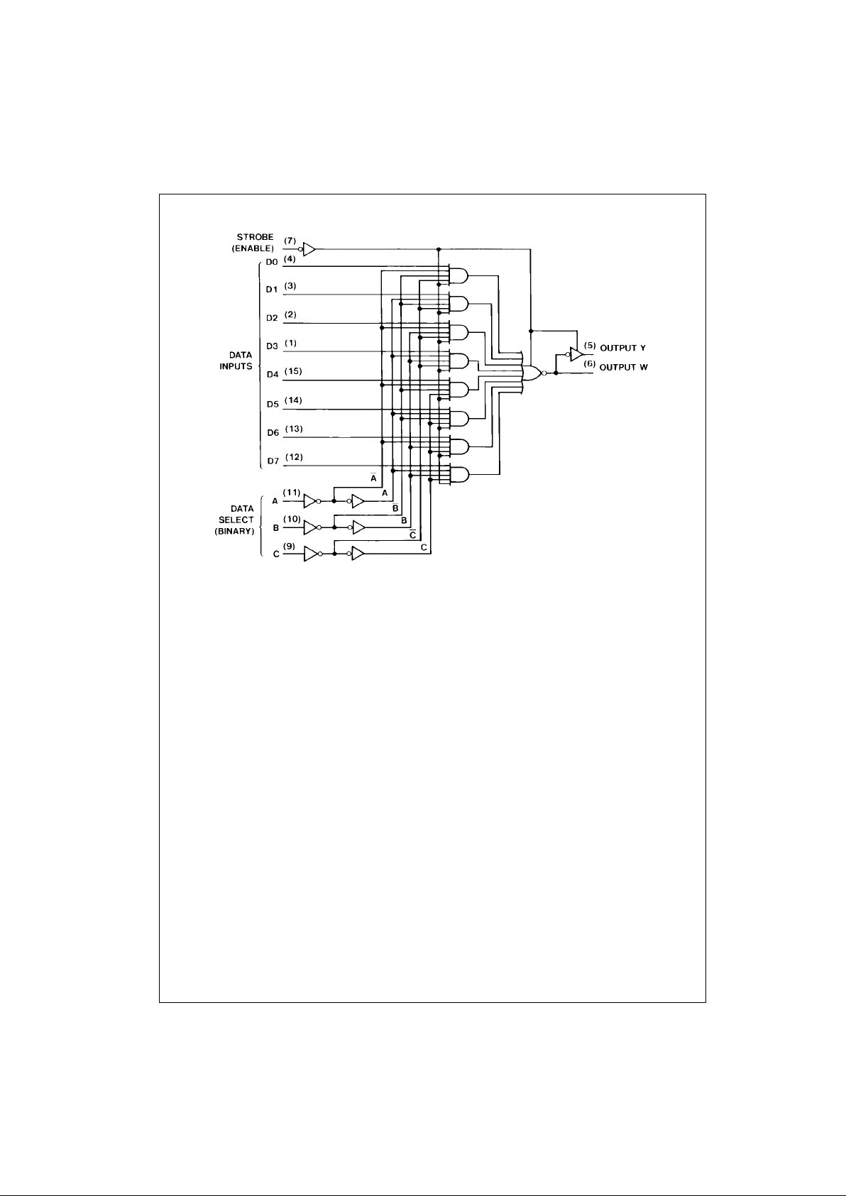
Logic Diagram
Page 3

3 www.fairchildsemi.com
DM74LS251
Absolute Maximum Ratings(Note 1)
Note 1: The “Absolute Maximum Ratings ” are those val ues beyond w hich
the safety of the device cannot be guaranteed. The device should not be
operated at thes e limits. The paramet ric values defined in the “Electrical
Characteristics” ta ble are not guaranteed at the absolute maxim um ratings.
The “Recommend ed O peratin g Cond itions” t able w ill defin e the condition s
for actual device operation.
Recommended Operating Conditions
Electrical Characteristics
over recommended operating free air temperature range (unless otherwise noted)
Note 2: All typicals are at VCC = 5V, TA = 25°C.
Note 3: Not more than one output should be shorted at a time, and the duration should not exceed one second.
Note 4: I
CC1
is measured with the outputs open, STROBE grounded, and all oth er inputs at 4.5V.
Note 5: I
CC2
is measured with the outputs open and all inp ut s at 4. 5V.
Supply Voltage 7V
Input Voltage 7V
Operating Free Air Temperature Range 0°C to +70°C
Storage Temperature Range −65°C to +150°C
Symbol Parameter Min Nom Max Units
V
CC
Supply Voltage 4.75 5 5.25 V
V
IH
HIGH Level Input Voltage 2 V
V
IL
LOW Level Input Volta ge 0.8 V
I
OH
HIGH Level Output Current −2.6 mA
I
OL
LOW Level Output Current 24 mA
T
A
Free Air Operating Temperature 0 70 °C
Symbol Parameter Conditions Min
Typ
Max Units
(Note 2)
V
I
Input Clamp Voltage VCC = Min, II = −18 mA −1.5 V
V
OH
HIGH Level VCC = Min, IOH = Max
2.4 3.1 V
Output Voltage VIL = Max, VIH = Min
V
OL
LOW Level VCC = Min, IOL = Max
0.35 0.5
Output Voltage VIL = Max, VIH = Min V
IOL = 12 mA, VCC = Min 0.25 0.4
I
I
Input Current @ Max Input Voltage VCC = Max, VI = 7V 0.1 mA
I
IH
HIGH Level Input Current VCC = Max, VI = 2.7V 20 µA
I
IL
LOW Level Input Current VCC = Max, VI = 0.4V −0.4 mA
I
OZH
Off-State Output Current with VCC = Max, VO = 2.7V
20 µA
HIGH Level Output Voltage Applied VIH = Min, VIL = Max
I
OZL
Off-State Output Current with VCC = Max, VO = 0.4V
−20 µA
LOW Level Output Voltage Applied VIH = Min, VIL = Max
I
OS
Short Circuit Output Current VCC = Max (Note 3) −20 −100 mA
I
CC1
Supply Current VCC = Max (Note 4) 6.1 10 mA
I
CC2
Supply Current VCC = Max (Note 5) 7.1 12 mA
Page 4

www.fairchildsemi.com 4
DM74LS251
Switching Characteristics
at VCC = 5V and TA = 25°C
Note 6: CL = 5 pF
From (Input) RL = 667Ω
Symbol Parameter
to (Output)
CL = 45 pF CL = 150 pF Units
Min Max Min Max
t
PLH
Propagation Delay Time A, B, C
45 53 ns
LOW-to-HIGH Level Output (4 Levels) to Y
t
PHL
Propagation Delay Time A, B, C
45 53 ns
HIGH-to-LOW Level Output (4 Levels) to Y
t
PLH
Propagation Delay Time A, B, C
33 38 ns
LOW-to-HIGH Level Output (3 Levels) to W
t
PHL
Propagation Delay Time A, B, C
33 42 ns
HIGH-to-LOW Level Output (3 Levels) to W
t
PLH
Propagation Delay Time
D to Y 28 35 ns
LOW-to-HIGH Level Output
t
PHL
Propagation Delay Time
D to Y 28 38 ns
HIGH-to-LOW Level Output
t
PLH
Propagation Delay Time
D to W 15 25 ns
LOW-to-HIGH Level Output
t
PHL
Propagation Delay Time
D to W 15 25 ns
HIGH-to-LOW Level Output
t
PZH
Output Enable Time to
Strobe to Y 45 60 ns
HIGH Level Output
t
PZL
Output Enable Time to
Strobe to Y 40 51 ns
LOW Level Output
t
PHZ
Output Disable Time from
Strobe to Y 45 ns
HIGH Level Output (Note 6)
t
PLZ
Output Disable Time from
Strobe to Y 25 ns
LOW Level Output (Note 6)
t
PZH
Output Enable Time to
Strobe to W 27 40 ns
HIGH Level Output
t
PZL
Output Enable Time to
Strobe to W 40 47 ns
LOW Level Output
t
PHZ
Output Disable Time from
Strobe to W 55 ns
HIGH Level Output (Note 6)
t
PLZ
Output Disable Time from
Strobe to W 25 ns
LOW Level Output (Note 6)
Page 5

5 www.fairchildsemi.com
DM74LS251
Physical Dimensions inches (millimeters) unless otherwise noted
16-Lead Small Outline Integrated Circuit (SOIC), JEDEC MS-012, 0.150 Narrow
Package Number M16A
Page 6

www.fairchildsemi.com 6
DM74LS251 3-STATE 1-of-8 Line Data Selector/Multiplexer
Physical Dimensions inches (millimeters) unless otherwise noted (Continued)
16-Lead Plastic Dual-In-Line Package (PDIP), JEDEC MS-001, 0.300 Wide
Package Number N16E
Fairchild does not assume any responsibility for use of any circuitry described, no circuit pate nt licenses are implied and
Fairchild reserves the right at any time without notice to change said circuitry and specifications.
LIFE SUPPORT POLICY
FAIRCHILD’S PRODUCTS ARE NOT AUTHORIZED FOR USE AS CRITICAL COMPONENTS IN LIFE SUPPORT
DEVICES OR SYSTEMS WITHOUT THE EXPRESS WRITTEN APPROVAL OF THE PRESIDENT OF FAIRCHILD
SEMICONDUCTOR CORPORATION. As used herein:
1. Life support devices or systems are devices or syste ms
which, (a) are intended for surgical implant into the
body, or (b) support or sustain life, and (c) whose failure
to perform when properly used in accordance with
instructions for use provided in the labeling, can be reasonably expected to result in a significant inju ry to the
user.
2. A critical component in any com ponen t of a life su pport
device or system whose failu re to perform can be reasonably expected to ca use the fa i lure of the life su pp ort
device or system, or to affect its safety or effectiveness.
www.fairchildsemi.com
 Loading...