

Page 1
August 1986
Revised March 2000
DM74LS244
Octal 3-STATE Buffer/Line Driver/Line Receiver
DM74LS244 Octal 3-STATE Buffer/Line Driver/Line Receiver
General Description
These buffers/line drivers are designed to improve both the
performance and PC board density of 3-STATE buffers/
drivers employed as memor y-address drivers, clock drivers, and bus-oriented transmitters/receivers. Featuring 400
mV of hysteresis at each low cu rrent PNP data lin e input,
they provide improve d nois e re jection and h igh fanout outputs and can be used to drive terminated l ines down to
133Ω.
Features
■ 3-STATE outputs drive bus lines directly
■ PNP inputs reduce DC loading on bus lines
■ Hysteresis at data inputs improves noise margins
■ Typical I
■ Typical I
■ Typical propagation delay times
■ Typical enable/disable time 18 ns
■ Typical power dissipation (enabled)
(sink curr ent) 24 mA
OL
(source current) −15 mA
OH
Inverting 10.5 ns
Noninverting 12 ns
Inverting 130 mW
Noninverting 135 mW
Ordering Code:
Order Number Package Number Package Description
DM74LS244W M M20B 20-Lead Small Outline Integrated Circui t (SOIC), JEDEC MS-013, 0.300 Wide
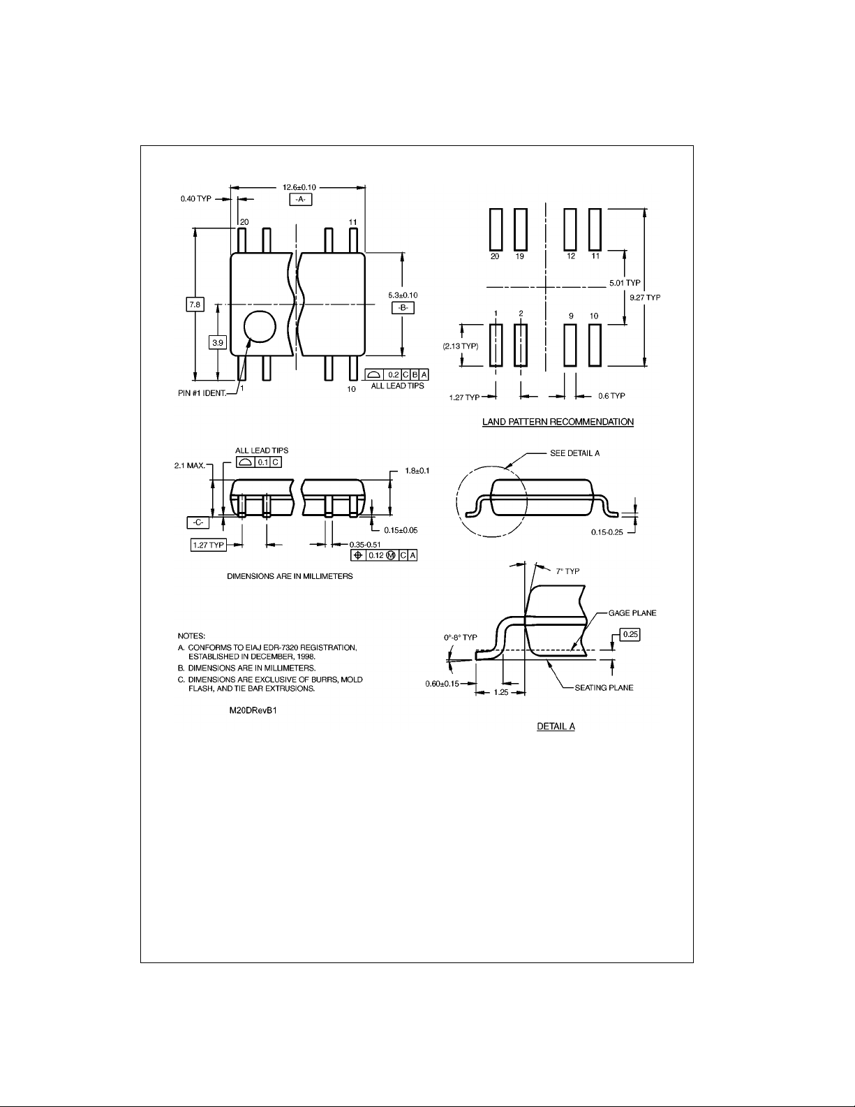
DM74LS244SJ M20D 20-Lead Small Outline Package (SOP), EIAJ TYPE II, 5.3mm Wide
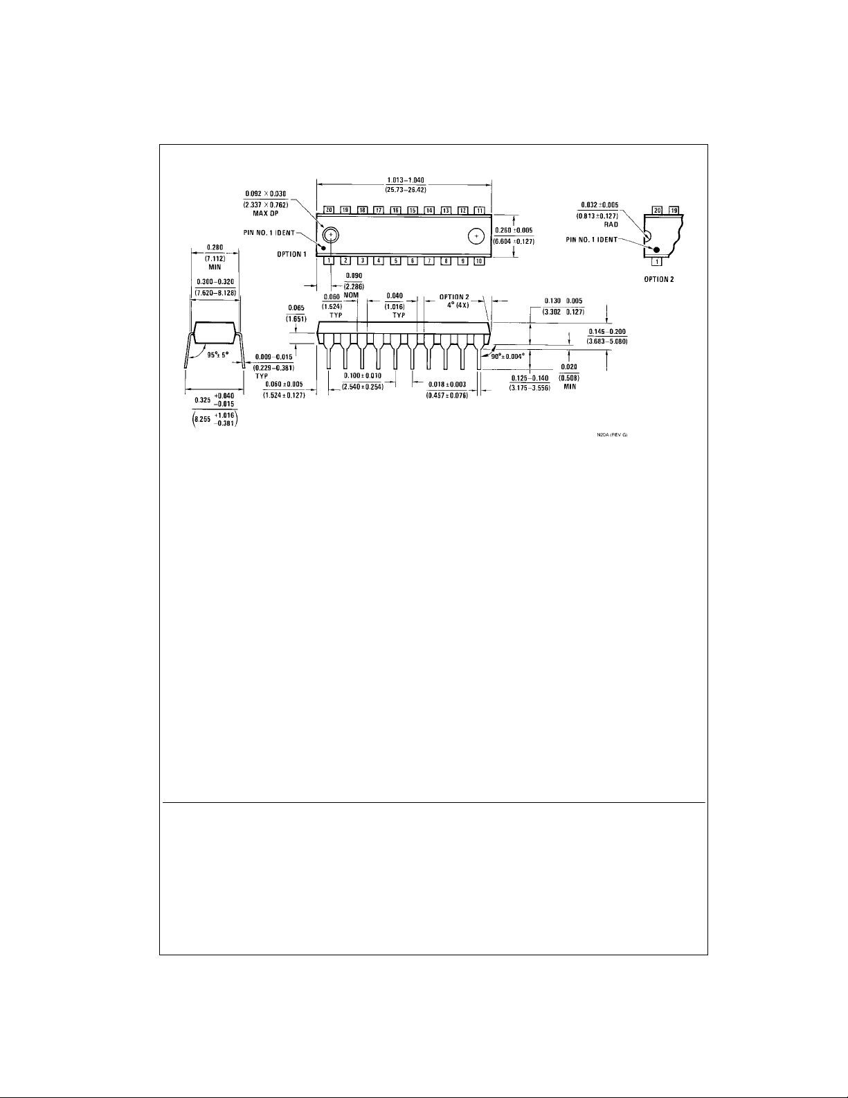
DM74LS244N N20A 20-Lead Plastic Dual-In-Line Package (PDIP), JEDEC MS-001, 0.300 Wide
Devices also availab le in Tape and Reel. Specify by appending th e s uffix let t er “X” to the ordering cod e.
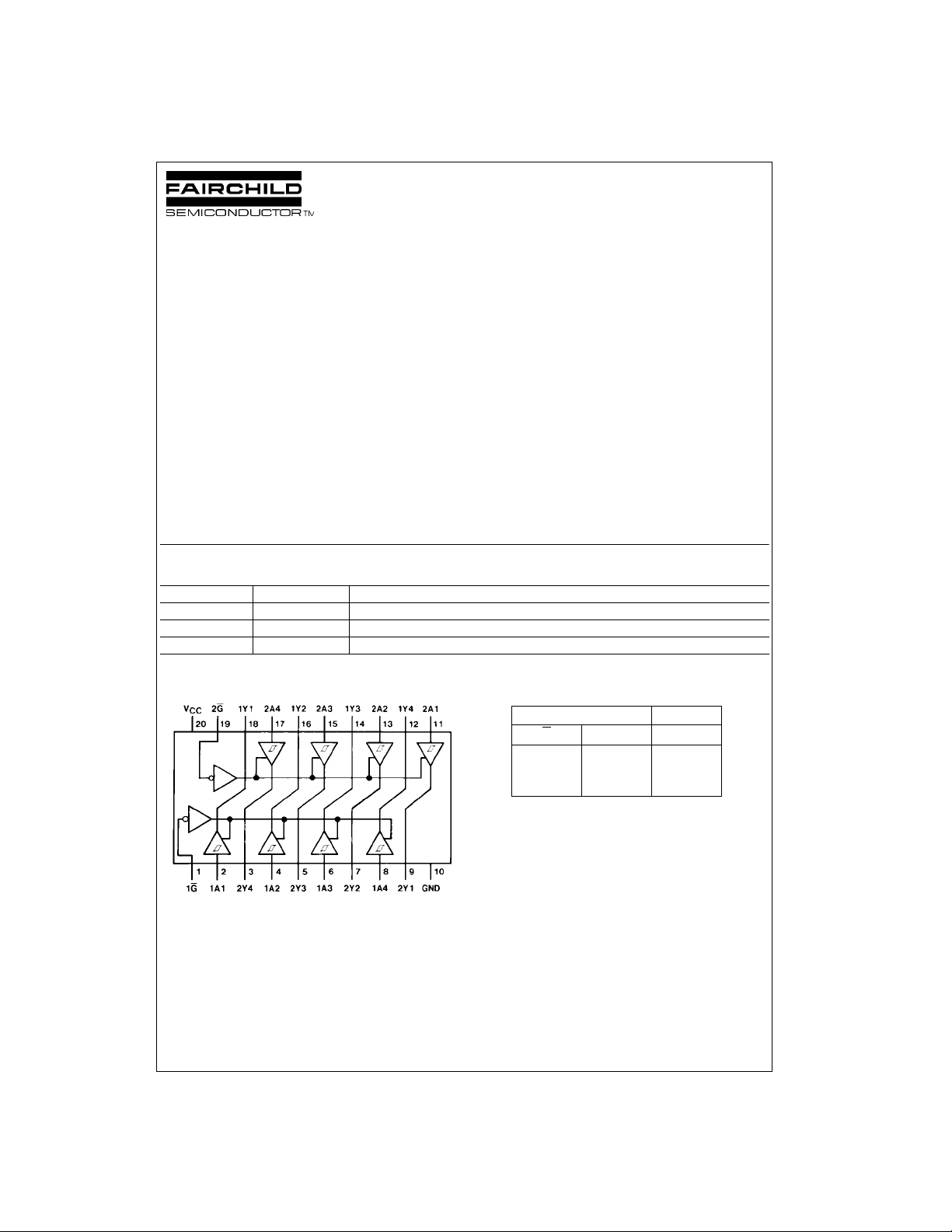
Connection Diagram Function Table
Inputs Output
G
LLL
LHH
L = LOW Logic Level
H = HIGH Logic Level
X = Either LOW or HIGH Logic Level
Z = High Impedance
HXZ
AY
© 2000 Fairchild Semiconductor Corporation DS008442 www.fairchildsemi.com
Page 2
Absolute Maximum Ratings(Note 1)
Supply Voltage 7V
Input Voltage 7V
Operating Free Air Temperature Range 0°C to +70°C
DM74LS244
Storage Temperature Range −65°C to +150°C
Note 1: The “Absolute Maximum Ratin gs” are those v alues beyon d which
the safety of the dev ice cannot be guaranteed. T he device sh ould not be
operated at these limits. The parametric values defined in the Electrical
Characteristics tables are not guaranteed at the absolute maximum ratings.
The “Recommend ed O peratin g Cond itions” t able w ill defin e the c ondit ions
for actual device operation.
Recommended Operating Conditions
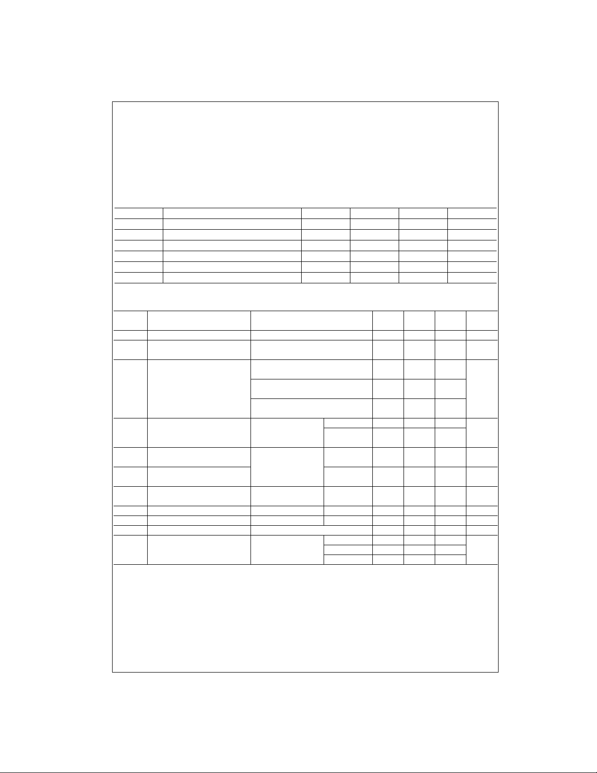
Symbol Parameter Min Nom Max Units
V
CC
V
IH
V
IL
I
OH
I
OL
T
A
Supply Voltage 4.75 5 5.25 V
HIGH Level Input Voltage 2 V
LOW Level In put Voltage 0.8 V
HIGH Level Output Current −15 mA
LOW Level Output Current 24 mA
Free Air Oper ating Temperature 0 70 °C
Electrical Characteristics
over recommended operating free air temperature range (unless otherwise noted)
Symbol Parameter Conditions
V
I
HYS Hysteresis (VT+ − VT−)V
V
OH
V
OL
I
OZH
I
OZL
I
I
I
IH
I
IL
I
OS
I
CC
Note 2: All typicals are at VCC = 5V, TA = 25°C.
Note 3: Not more than one output should be shorted at a time, and the duration should not exceed one second.
Input Clamp Voltage VCC = Min, II = −18 mA −1.5 V
Data Inputs Only
HIGH Level Output Voltage VCC = Min, VIH = Min
LOW Level Output Voltage VCC = Min IOL = 12 mA 0.4
Off-State Output Current, VCC = Max VO = 2.7V 20 µA
HIGH Level Voltage Applied VIL = Max
Off-State Output Current, VIH = Min VO = 0.4V −20 µA
LOW Level Voltage Applied
Input Current at Maximum VCC = Max VI = 7V 0.1 mA
Input Voltage
HIGH Level Input Current VCC = Max VI = 2.7V 20 µA
LOW Level Input Current VCC = Max VI = 0.4V −0.5 −200 µA
Short Circuit Output Current VCC = Max (Note 3) −40 −225 mA
Supply Current VCC = Max, Outputs HIGH 13 23
= Min 0.2 0.4 V
CC
VIL = Max, IOH = −1 mA
VCC = Min, VIH = Min
VIL = Max, IOH = −3 mA
VCC = Min, VIH = Min
VIL = 0.5V, IOH = Max
VIH = Min
Outputs Open Outputs LOW 27 46 mA
Outputs Disabled 32 54
Min Typ Max
(Note 2)
2.7
2.4 3.4 V
2
Units
VVIL = Max IOL = Max 0.5
www.fairchildsemi.com 2
Page 3
Switching Characteristics
at VCC = 5V, TA = 25°C
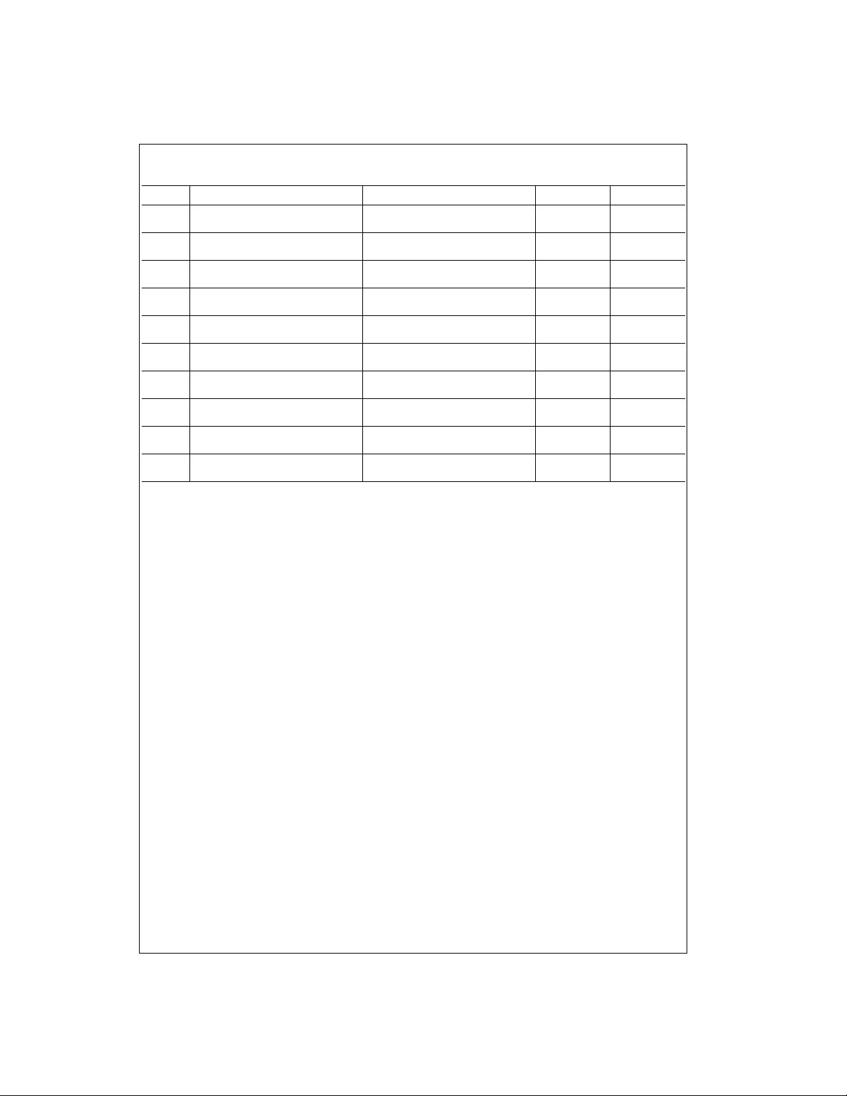
Symbol Parameter Conditions Max Units
t
t
t
t
t
t
t
t
t
t
PLH
PHL
PZL
PZH
PLZ
PHZ
PLH
PHL
PZL
PZH
Propagation Delay Time CL = 45 pF
LOW-to-HIGH Level Output RL = 667Ω
Propagation Delay Time CL = 45 pF
HIGH-to-LOW Level Output RL = 667Ω
Output Enable Time to CL = 45 pF
LOW Level RL = 667Ω
Output Enable Time to CL = 45 pF
HIGH Level RL = 667Ω
Output Disable Time CL = 5 pF
from LOW Level RL = 667Ω
Output Disable Time CL = 5 pF
from HIGH Level RL = 667Ω
Propagation Delay Time CL = 150 pF
LOW-to-HIGH Level Output RL = 667Ω
Propagation Delay Time CL = 150 pF
HIGH-to-LOW Level Output RL = 667Ω
Output Enable Time to CL = 150 pF
LOW Level RL = 667Ω
Output Enable Time to CL = 150 pF
HIGH Level RL = 667Ω
18 ns
18 ns
30 ns
23 ns
25 ns
18 ns
21 ns
22 ns
33 ns
26 ns
DM74LS244
3 www.fairchildsemi.com
Page 4
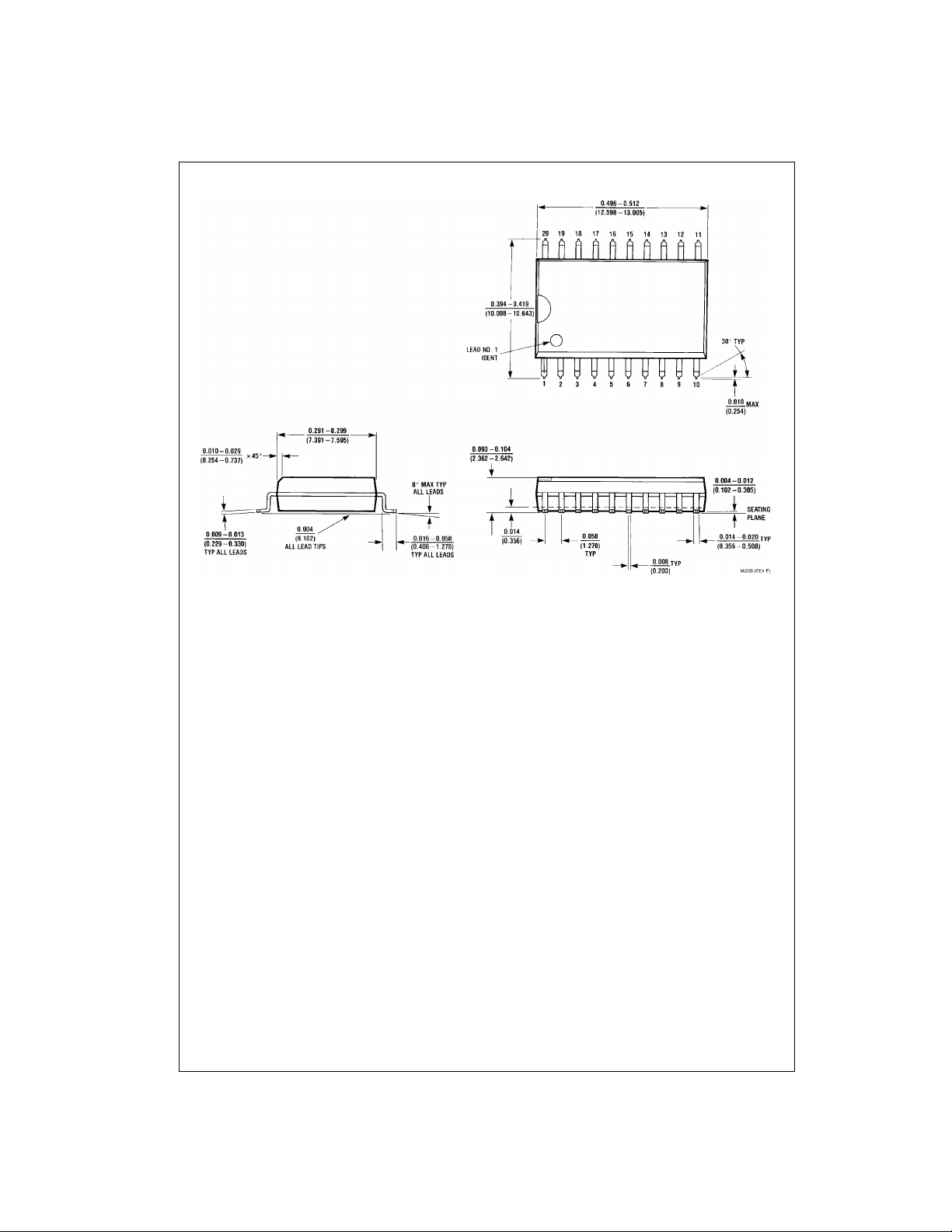
Physical Dimensions inches (millimeters) unless otherwise noted
DM74LS244
20-Lead Small Outline Integrated Circuit (SOIC), JEDEC MS-013, 0.300 Wide
Package Number M20B
www.fairchildsemi.com 4
Page 5
Physical Dimensions inches (millimeters) unless otherwise noted (Continued)
DM74LS244
20-Lead Small Outline Package (SOP), EIAJ TYPE II, 5.3mm Wide
Package Number M20D
5 www.fairchildsemi.com
Page 6
Physical Dimensions inches (millimeters) unless otherwise noted (Continued)
20-Lead Plastic Dual-In-Line Package (PDIP), JEDEC MS-001, 0.300 Wide
Package Number N20A
DM74LS244 Octal 3-STATE Buffer/Line Driver/Line Receiver
Fairchild does not assume any responsibility for us e of any circuitry described, no circuit patent licenses are implied and
Fairchild reserves the right at any time without notice to change said circuitry and specifications.
LIFE SUPPORT POLICY
FAIRCHILD’S PRODUCTS ARE NOT AUTHORIZED FOR USE AS CRITICAL COMPONENTS IN LIFE SUPPORT
DEVICES OR SYSTEMS WITHOUT THE EXPRESS WRITTEN APPROVAL OF THE PRESIDENT OF FAIRCHILD
SEMICONDUCTOR CORPORATION. As used herein:
1. Life support devices or systems are devices or syste ms
which, (a) are intended for surgical implant into the
body, or (b) support or sustain life, and (c) whose failure
to perform when properly used in accordance with
instructions for use provided in the labeling, can be reasonably expected to result in a significan t injury to the
user.
2. A critical component in any compon ent of a lif e supp ort
device or system whose failu re to perform can be reasonably expected to ca use the fa i lure of the li fe su pp ort
device or system, or to affect its safety or effectiveness.
www.fairchildsemi.com
www.fairchildsemi.com 6
 Loading...