

Datasheet DM74LS243WM, DM74LS243N, DM74LS243MX, DM74LS243M, DM74LS243WMX Datasheet (Fairchild Semiconductor)
© 2000 Fairchild Semiconductor Corporation DS006412 www.fairchildsemi.com
August 1986
Revised January 2000
DM74LS243 Quadruple Bus Transceiver
DM74LS243
Quadruple Bus Transcei ver
General Description
This four data line transceiver is designed for asyn chronous two-way communication s betw een dat a buses. It can
be used to drive terminated lines down to 133Ω.
Features
■ Two-way asynchronous communication between data
buses
■ PNP inputs reduce DC loading on bus line
■ Hysteresis at data inputs improves noise margin
Ordering Code:
Devices also availab le in Tape and Reel. Specify by appending th e s uffix let t er “X” to the ordering code.
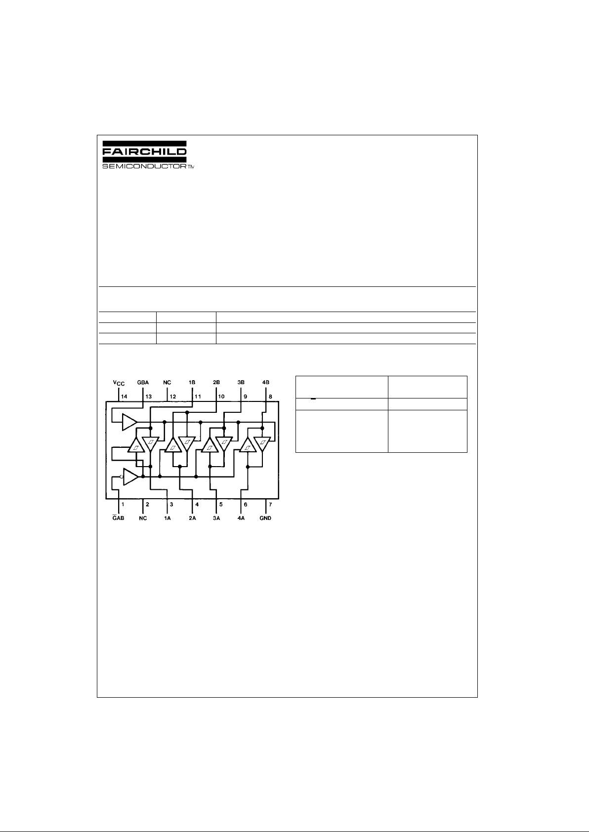
Connection Diagram Function Table
I = Input
O = Output
H = HIGH Logic Level
L = LOW Logic Level
Note 1: Possibly destructive osc illation may occ ur if the transc eivers are
enabled in both direc t ions at once.
Order Number Package Number Package Description
DM74LS243M M14A 14-Lead Small Outline Integrated Circuit (SOIC), JEDEC MS-120, 0.150 Narrow
DM74LS243N N14A 14-Lead Plastic Dual-In-Line Package (PDIP), JEDEC MS-001, 0.300 Wide
Control Data Port
Inputs Status
G
AB GBA A B
HHOI
L H (Note 1) (Note 1)
H L ISOLATED
LLIO
www.fairchildsemi.com 2
DM74LS243
Absolute Maximum Ratings(Note 2)
Note 2: The “Absolute Maximum Ratings” are those values beyond which
the safety of the dev ice cannot be guaranteed. T he device sh ould not be
operated at these limits. The parametric values defined in the Electrical
Characteristics tables are not guaranteed at the absolute maximum ratings.
The “Recommend ed O peratin g Cond itions” t able w ill defin e the co ndition s
for actual device operation.
Recommended Operating Conditions
Electrical Characteristics
over recommended operating free air temperature range (unless otherwise noted)
Note 3: All typicals are at VCC = 5V, TA = 25°C.
Note 4: Not more than one output should be shorted at a time, and the duration should not exceed one second.
Supply Voltage 7V
Input Voltage
Any G 7V
A or B 5.5V
Operating Free Air Temperature Range 0°C to +70°C
Storage Temperature Range −65°C to +150°C
Symbol Parameter Min Nom Max Units
V
CC
Supply Voltage 4.75 5 5.25 V
V
IH
HIGH Level Input Voltage 2 V
V
IL
LOW Level Input Voltage 0.8 V
I
OH
HIGH Level Output Current −15 mA
I
OL
LOW Level Output Current 24 mA
T
A
Free Air Operating Temperature 0 70 °C
Symbol Parameter Conditions Min
Typ
Max Units
(Note 3)
V
I
Input Clamp Voltage VCC = Min, II = −18 mA −1.5 V
HYS Hysteresis (VT+ − VT−)V
CC
= Min 0.2 0.4 V
(Data Inputs Only)
V
OH
HIGH Level Output Voltage VCC = Min, VIH = Min 2.7
VIL = Max, IOH = −1 mA
VCC = Min, VIH = Min 2.4 3.4 V
VIL = Max, IOH = −3 mA
VCC = Min, VIH = Min 2
VIL = 0.5V, IOH = Max
V
OL
LOW Level Output Voltage VCC = Min IOL = 12 mA 0.4
VIL = Max IOL = Max V
VIH = Min 0.5
I
OZH
Off-State Output Current, VCC = Max VO = 2.7V 40 µA
HIGH Level Voltage Applied VIL = Max
I
OZL
Off-State Output Current, VIH = Min VO = 0.4V −200 µA
LOW Level Voltage Applied
I
I
Input Current at Maximum VCC = Max VI = 5.5V A or B 0.1 mA
Input Voltage VI = 7V Any G 0.1 mA
I
IH
HIGH Level Input Current VCC = Max, VI = 2.7V 20 µA
I
IL
LOW Level Input Current VCC = Max, VI = 0.4V −0.2 mA
I
OS
Short Circuit Output Current VCC = Max (Note 4) −40 −225 mA
I
CC
Supply Current VCC = Max Outputs HIGH 22 38
Outputs Outputs LOW 29 50 mA
OPEN Outputs Disabled 32 54

3 www.fairchildsemi.com
DM74LS243
Switching Characteristics
at VCC = 5V, TA = 25°C
Symbol Parameter Conditions Min Max Units
t
PLH
Propagation Delay Time CL = 45 pF
18 ns
LOW-to-HIGH Level Output RL = 667Ω
t
PHL
Propagation Delay Time CL = 45 pF
18 ns
HIGH-to-LOW Level Output RL = 667Ω
t
PZL
Output Enable Time CL = 45 pF
30 ns
to LOW Level RL = 667Ω
t
PZH
Output Enable Time CL = 45 pF
23 ns
to HIGH Level RL = 667Ω
t
PLZ
Output Disable Time CL = 5 pF
25 ns
from LOW Level RL = 667Ω
t
PHZ
Output Disable Time CL = 5 pF
18 ns
from HIGH Level RL = 667Ω
t
PLH
Propagation Delay Time CL = 150 pF
21 ns
LOW-to-HIGH Level Output RL = 667Ω
t
PHL
Propagation Delay Time CL = 150 pF
22 ns
HIGH-to-LOW Level Output RL = 667Ω
t
PZL
Output Enable Time CL = 150 pF
33 ns
to LOW Level RL = 667Ω
t
PZH
Output Enable Time CL = 150 pF
26 ns
to HIGH Level RL = 667Ω

www.fairchildsemi.com 4
DM74LS243
Physical Dimensions inches (millimeters) unless otherwise noted
14-Lead Small Outline Integrated Circuit (SOIC), JEDEC MS-120, 0.150 Narrow
Package Number M14A

5 www.fairchildsemi.com
DM74LS243 Quadruple Bus Transceiver
Physical Dimensions inches (millimeters) unless otherwise noted (Continued)
14-Lead Plastic Dual-In-Line Package (PDIP), JEDEC MS-001, 0.300 Wide
Package Number N14A
Fairchild does not assume any responsibility for use of any circu itry described, no circuit patent license s are implied and
Fairchild reserves the right at any time without notice to change said circuitry and specifications.
LIFE SUPPORT POLICY
FAIRCHILD’S PRODUCTS ARE NOT AUTHORIZED FOR USE AS CRITICAL COMPONENTS IN LIFE SUPPORT
DEVICES OR SYSTEMS WITHOUT THE EXPRESS WRITTEN APPROVAL OF THE PRESIDENT OF FAIRCHILD
SEMICONDUCTOR CORPORATION. As used herein:
1. Life support devices or systems are dev ic es or syste ms
which, (a) are intended for surgical implant into the
body, or (b) support or sustain life, and (c) whose failure
to perform when properly used in accordance with
instructions for use provided i n the labe li ng, can be re asonably expected to result in a significant injury to the
user.
2. A critical componen t in any com ponent o f a l ife supp ort
device or system whose failu re to perform can b e reasonably expected to c ause th e fa i lure of the li fe s upp or t
device or system, or to affect its safety or effectiveness.
www.fairchildsemi.com
 Loading...