

Datasheet DM74LS193N, DM74LS193MX, DM74LS193M, DM74LS193CW Datasheet (Fairchild Semiconductor)
Page 1
© 2000 Fairchild Semiconductor Corporation DS006406 www.fairchildsemi.com
September 1986
Revised March 2000
DM74LS193 Synchronous 4-Bit Binary Counter with Dual Clock
DM74LS193
Synchronous 4-Bit Binary Counter with Dual Clock
General Description
The DM74LS193 circuit is a synchronous up/down 4-bit
binary counter. Synchronous oper ation i s pro vide d by ha ving all flip-flops c locked sim ult a neo usly, so that the o utp uts
change together when so instr ucted by the steering logic.
This mode of operation eliminates the output counting
spikes normally associated with asynchronous (rippleclock) counters.
The outputs of the four master-slave flip-flops are triggered
by a LOW-to-HIGH level transition of either count (clock)
input. The direction of counting is determined by which
count input is pulsed while the oth er count input is held
HIGH.
The counter is fully programmable; that is, each output may
be preset to either le vel b y en ter ing the de si red da ta at t he
inputs while the load inpu t is LOW. The output will ch ange
independently of the count pul ses. This feat ure allows t he
counters to be used as modulo-N divi ders by simply mo difying the count length with the preset inputs.
A clear input has been pr ovided which, when taken to a
high level, forces all out puts to the low leve l; independent
of the count and load in puts. The clear, count, and load
inputs are buffered to lower the driv e req uire me nts of clock
drivers, etc., required for long words.
These counters we re d esign ed to be cascaded witho ut the
need for external circu itry. Both borrow and carry outputs
are available to cascade both th e up and down counting
functions. The borrow output produces a pulse equal in
width to the count down input when the counter underflows.
Similarly, the carry output produces a pulse equ al in width
to the count d own in pu t when an overf low condition exists.
The counters can the n be easily cascaded b y feeding the
borrow and carr y outputs to th e count d own and cou nt up
inputs respectively of the succeeding counter.
Features
■ Fully independent clear input
■ Synchronous operation
■ Cascading circuitry provided internally
■ Individual preset each flip-flop
Ordering Code:
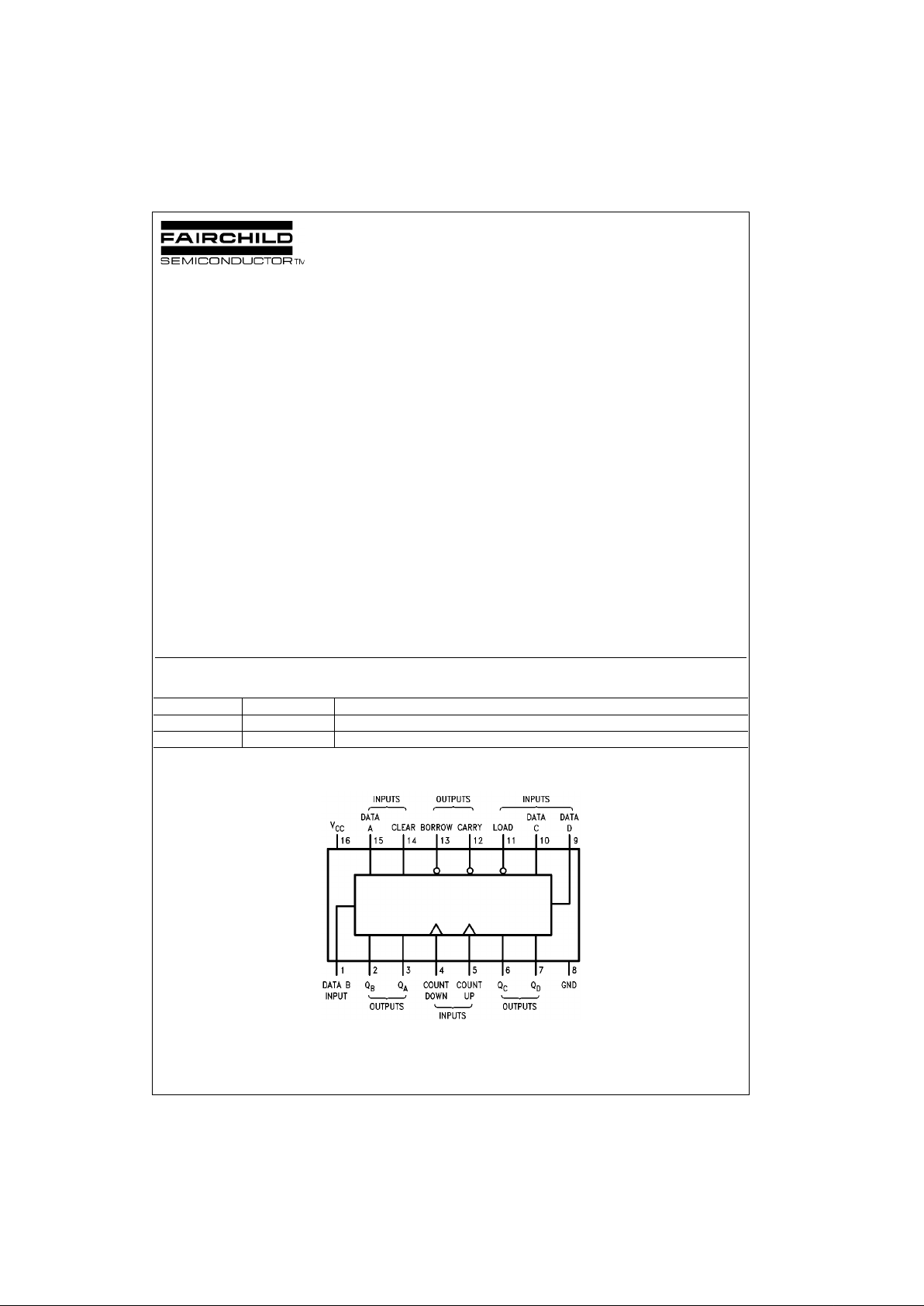
Connection Diagram
Order Number Package Number Package Description
DM74LS193M M16A 16-Lead Small Outline Integrated Circuit (SOIC), JEDEC MS-012, 0.150” Narrow Body
DM74LS193N N16E 16-Lead Plastic Dual-In-Line Package (PDIP), JEDEC MS-001, 0.300” Wide
Page 2
www.fairchildsemi.com 2
DM74LS193
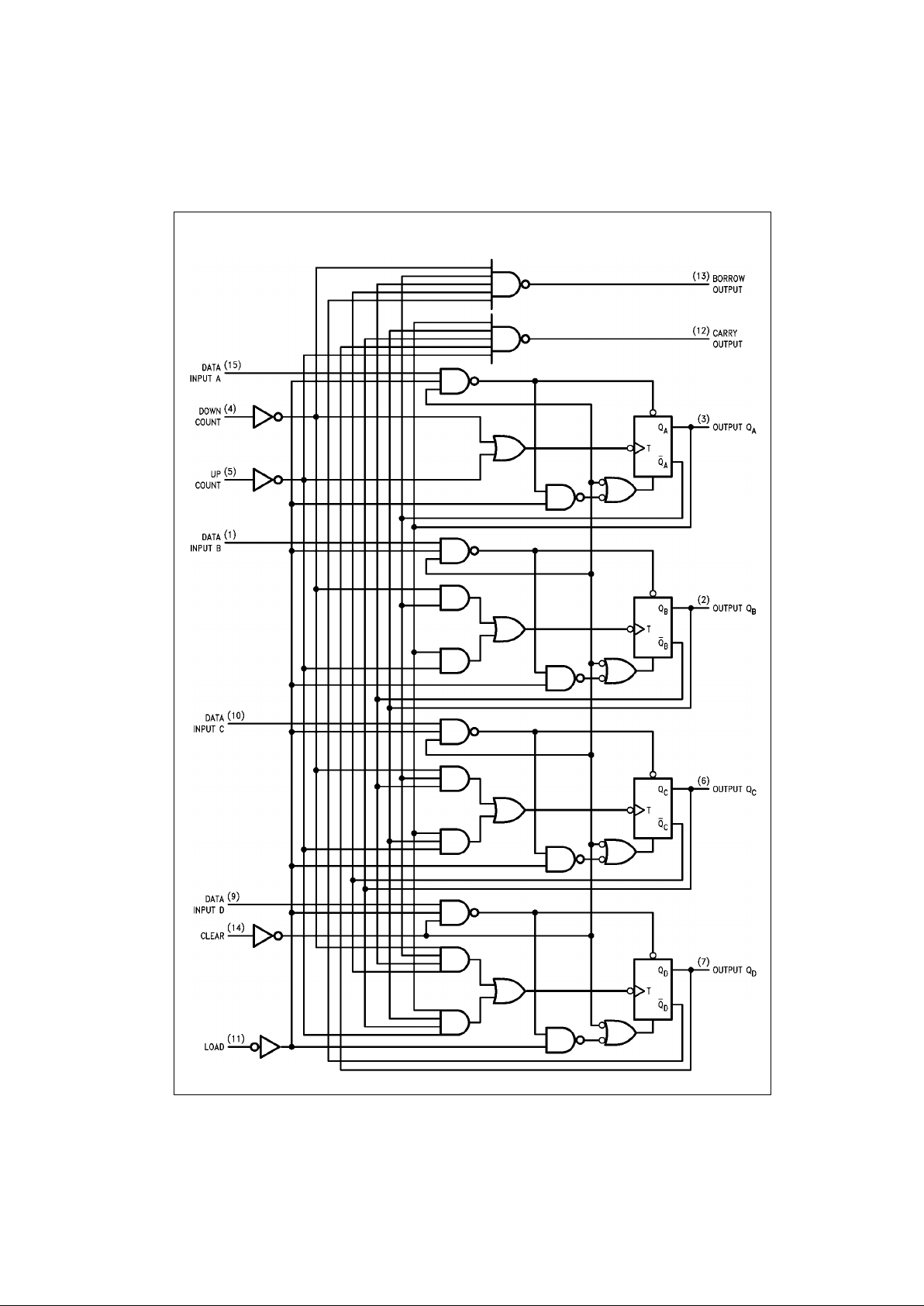
Logic Diagram
Page 3
3 www.fairchildsemi.com
DM74LS193
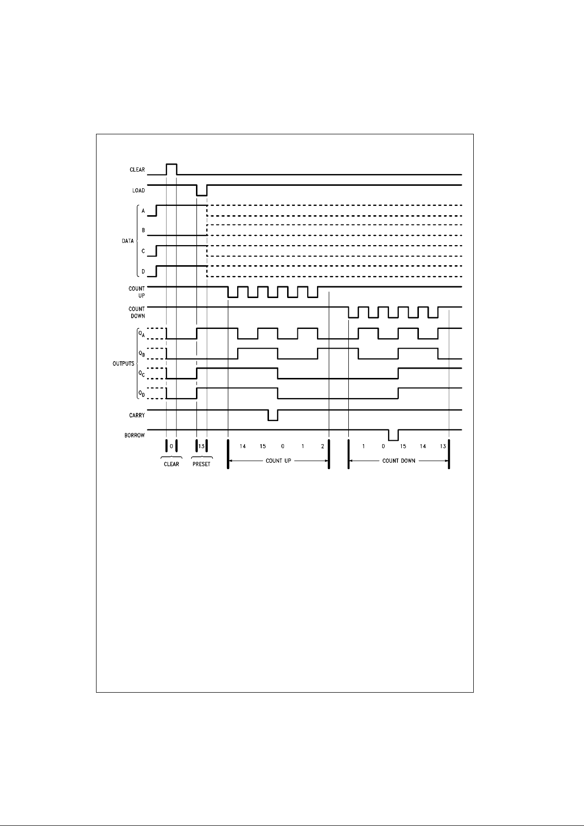
Timing Diagram
Note A: Clear overrides load, data, and count inputs
Note B: When counting up, count-down input must be HIGH; when counting down, count-up input must be HIGH.
Page 4

www.fairchildsemi.com 4
DM74LS193
Absolute Maximum Ratings(Note 1)
Note 1: The “Absolute Maximum Ratin gs” are those v alues beyon d which
the safety of the dev ice cannot be guaranteed. T he device sh ould not be
operated at these limits. The parametric values defined in the Electrical
Characteristics tables are not guaranteed at the absolute maximum ratings.
The “Recommend ed O peratin g Cond itions” t able w ill defin e the co ndition s
for actual device operation.
Recommended Operating Conditions
Note 2: CL = 15 pF, RL = 2 kΩ, IA = 25°C and VCC = 5V.
Note 3: C
L
= 50 pF, RL = 2 kΩ, IA = 25°C and VCC = 5V.
Note 4: T
A
= 25°C and VCC = 5V.
DC Electrical Characteristics
Note 5: All typicals are at VCC = 5V, TA = 25°C.
Note 6: Not more than one output should be shorted at a time, and the duration should not exceed one second.
Note 7: I
CC
is measured with all out puts open, CLEAR an d LOAD inputs ground ed, and all other inputs at 4. 5V.
Operating Free Air Temperature Range −0°C to +70°C
Supply Voltage 7V
Input Voltage 7V
Storage Temperature Range −65°C to +125°C
Symbol Parameter Min Nom Max Units
V
CC
Supply Voltage 4.75 5 5.25 V
V
IH
HIGH Level Input Voltage 2 V
V
IL
LOW Level Input Voltage 0.8 V
I
OH
HIGH Level Output Current −0.4 mA
I
OL
LOW Level Output Current 8 mA
f
CLK
Clock Frequency (Note 2) 0 25
MHz
Clock Frequency (Note 3)
t
W
Pulse Width of any Input (Note 4) 20 ns
t
SU
Data Setup Time (Not e 4) 20 ns
t
H
Data Hold Time (Note 4) 0 ns
t
EN
Enable Time to Clock (Note 4) 40 ns
T
A
Free Air Operating Temperature 0 70 °C
Symbol Parameter Conditions
Min Typ Max
Units
(Note 5)
V
I
Input Clamp Voltage VCC = Min, II = −18 mA −1.5 V
V
OH
HIGH Level Output VCC= Min, IOH= Max 2.5 3.4
V
Voltage VIL = Max, VIH = Min 2.7 3.4
V
OL
LOW Level Output VCC= Min, IOL= Max 0.25 0.4
Voltage VIL = Max, VIH = Min 0.35 0.5 V
IOL= 4mA,VCC= Min 0.25 0.4
I
I
Input Current @ Max Input Voltage VCC = Max, VI = 7V 0.1 mA
I
IH
HIGH Level Input Current VCC = Max, VI = 2.7V 20 µA
I
IL
LOW Level Input Current VCC = Max, VI = 0.4V −0.4 mA
I
OS
Short Circuit VCC = Max −20 −100
mA
Output Current (Note 6) −20 −100
I
CC
Supply Current VCC = Max (Note 7) 19 34 mA
Page 5

5 www.fairchildsemi.com
DM74LS193
AC Electrical Characteristics
From (Input)
RL = 2 kΩ
Symbol Parameter
To (Output)
CL = 15 pF CL = 50 pF Units
MinMaxMinMax
f
MAX
Maximum Clock Frequency 25 20 MHz
t
PLH
Propagation Delay Time Count Up
26 30 ns
LOW-to-HIGH Level Output to Carry
t
PHL
Propagation Delay Time Count Up
24 36 ns
HIGH-to-LOW Level Output to Carry
t
PLH
Propagation Delay Time Count Down
24 29 ns
LOW-to-HIGH Level Output to Borrow
t
PHL
Propagation Delay Time Count Down
24 32 ns
HIGH-to-LOW Level Output to Borrow
t
PLH
Propagation Delay Time Either Count
38 45 ns
LOW-to-HIGH Level Output to Any Q
t
PHL
Propagation Delay Time Either Count
47 54 ns
HIGH-to-LOW Level Output to Any Q
t
PLH
Propagation Delay Time Load to
40 41 ns
LOW-to-HIGH Level Output Any Q
t
PHL
Propagation Delay Time Load to
40 47 ns
HIGH-to-LOW Level Output Any Q
t
PHL
Propagation Delay Time Clear to
35 44 ns
HIGH-to-LOW Level Output Any Q
Page 6

www.fairchildsemi.com 6
DM74LS193
Physical Dimensions inches (millimeters) unless otherwise noted
16-Lead Small Outline Integrated Circuit (SOIC), JEDEC MS-012, 0150” Narrow Body
Package Number M16A
Page 7

Physical Dimensions inches (millimeters) unless otherwise noted (Continued)
7 www.fairchildsemi.com
DM74LS193 Synchronous 4-Bit Binary Counter with Dual Clock
Physical Dimensions inches (millimeters) unless otherwise noted (Continued)
16-Lead Plastic Dual-In-Line Package (PDIP), JEDEC MS-001, 0.300” Wide
Package Number N16E
Fairchild does not assume any responsibility for use of any circu itry described, no circuit patent license s are implied and
Fairchild reserves the right at any time without notice to change said circuitry and specifications.
LIFE SUPPORT POLICY
FAIRCHILD’S PRODUCTS ARE NOT AUTHORIZED FOR USE AS CRITICAL COMPONENTS IN LIFE SUPPORT
DEVICES OR SYSTEMS WITHOUT THE EXPRESS WRITTEN APPROVAL OF THE PRESIDENT OF FAIRCHILD
SEMICONDUCTOR CORPORATION. As used herein:
1. Life support devices or systems are dev ic es or syste ms
which, (a) are intended for surgical implant into the
body, or (b) support or sustain life, and (c) whose failure
to perform when properly used in accordance with
instructions for use provided i n the labe li ng, can be re asonably expected to result in a significant injury to the
user.
2. A critical componen t in any com ponent o f a l ife supp ort
device or system whose failu re to perform can b e reasonably expected to c ause th e fa i lure of the li fe s upp or t
device or system, or to affect its safety or effectiveness.
www.fairchildsemi.com
 Loading...