

Page 1
August 1986
Revised February 1999
DM74LS191 Synchronous 4-Bit Up/Down Counter with Mode Control
© 1999 Fairchild Semiconductor Corporation DS006405.prf www.fairchildsemi.com
DM74LS191
Synchronous 4-Bit Up/Down Counter with Mode Control
General Description
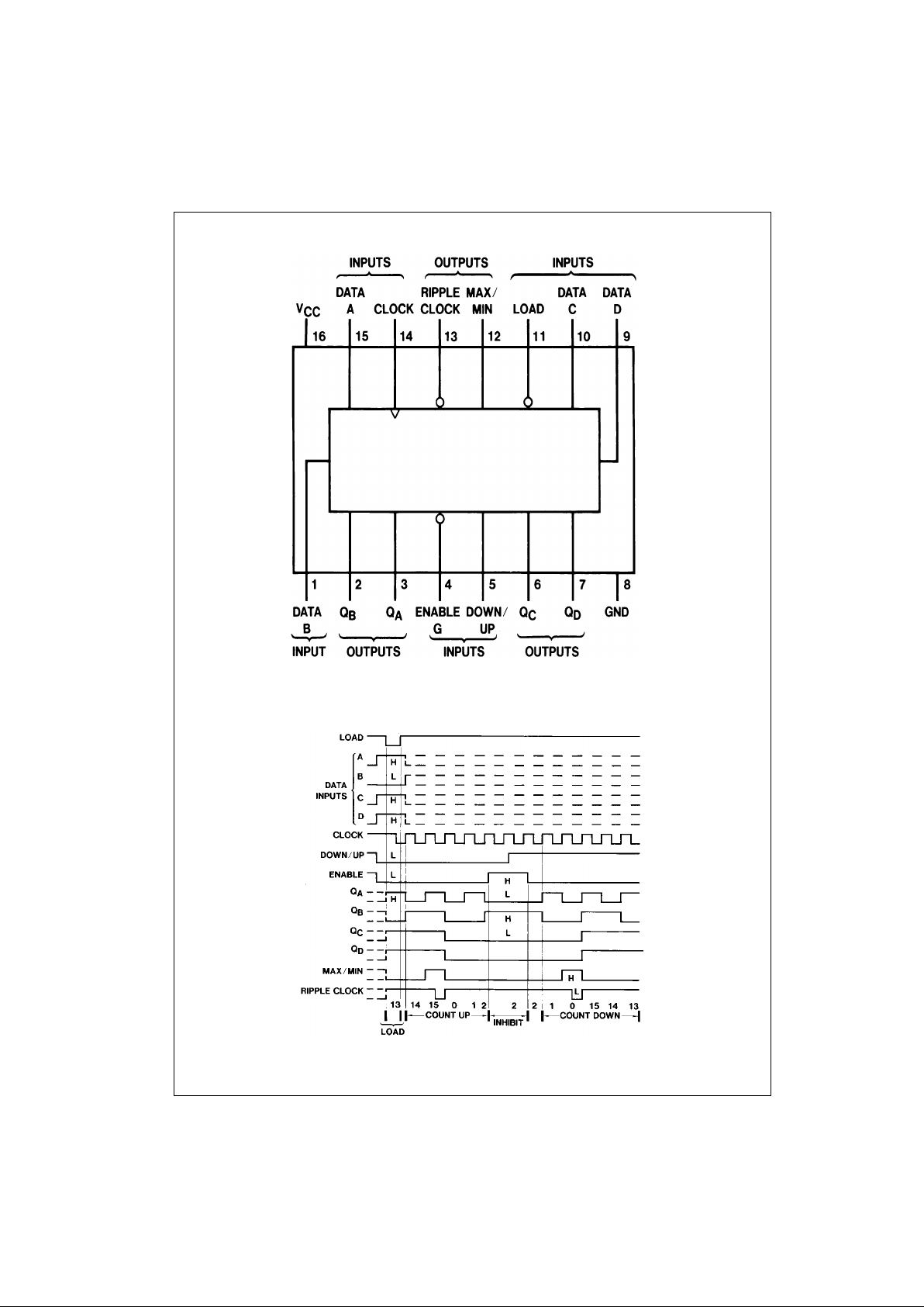
The DM74LS191 circ uit is a synchronous, reversible, up/
down counter. Synchronous operation is provided by having all flip-flops clocked simultaneou sly, so that the outputs
change simultaneously when so instructed by the steer ing
logic. This mode of operation eliminates the out put counting spikes normally associat ed with asynchronous (ripple
clock) counters.
The outputs of the four master-sl ave flip-flops are tr igg er ed
on a LOW-to-HIGH level transition of the clock input , if the
enable input is LOW. A HIGH at the enable input inhibits
counting. Level changes at either the enable input or the
down/up input should be made only when the clock input is
HIGH. The direction of the co unt is determined by the level
of the down/up input. When LOW, the counter counts up
and when HIGH, it counts down.
The counter is fully programmable; that is, the ou tpu ts m ay
be preset to either level by placing a LOW on the load input
and entering the desired data at the data inputs. The output
will change independent of the level of the clock input. This
feature allows the counters to be u sed as modu lo-N dividers by simply modifying the coun t length with the preset
inputs.
The clock, down/up, and load inpu ts are buffered to lower
the drive requirement; which significantly reduces the number of clock drivers, etc., required for long parallel words.
Two outputs have been made available to perform the cascading function: ripple clock and maximum/minimum count.
The latter output pro duces a hig h-level output pulse w ith a
duration approximately equal to one c omplete cycle of the
clock when the counter overflows or un der flows. The ripple
clock output produces a low-level output pulse equal in
width to the low-level portion of the clock input when an
overflow or underflow condition exists. The counters can be
easily cascaded by feeding the ripple clock output to the
enable input of the succeeding co unter if parallel clocking
is used, or to the clock input if parall el enabling is used.
The maximum/minimum count output can be used to
accomplish look-ahead for high-speed operation.
Features
■ Counts binary
■ Single down/up count control line
■ Count enable control input
■ Ripple clock output for cascading
■ Asynchronously presettable with load control
■ Parallel outputs
■ Cascadable for n-bit applications
■ Average propagation delay 20 ns
■ Typical clock frequency 25 MHz
■ Typical power dissipation 100 mW
Ordering Code:
Devices also available in Tape and Reel. Specify by appending the suffix letter “X” to the ordering code.
Order Number Package Number Package Description
DM74LS191M M16A 16-Lead Small Outline Integrated Circuit (SOIC), JEDEC MS-012, 0.150” Narrow Body
DM74LS191N N16E 16-Lead Plastic Dual-In-Line Package (PDIP), JEDEC MS-001, 0.300” Wide
Page 2
www.fairchildsemi.com 2
DM74LS191
Connection Diagram
Timing Diagram
Page 3

3 www.fairchildsemi.com
DM74LS191
Logic Diagram
Pin (16) = VCC, Pin (8) = GND
Page 4

www.fairchildsemi.com 4
DM74LS191
Absolute Maximum Ratings(Note 1)
Note 1: The “Absolute Maximum R atings” are t hose values b eyond which
the safety of the device cannot be guaranteed. T he device shou ld not be
operated at these limit s. The parametric values defined in the Electrical
Characteristics tables are not guaranteed at the absolute maximum ratings.
The “Recommend ed O perating Cond itions” t able wil l define the co ndition s
for actual device operation.
Recommended Operating Conditions
Note 2: TA = 25°C and VCC = 5V.
DC Electrical Characteristics
Note 3: All typicals are at VCC = 5V, TA = 25°C.
Note 4: Not more than one output should be shorted at a time, and the duration should not exceed one second.
Note 5: I
CC
is measured with all inputs grounded and all outputs open.
Storage Temperature Range −65°C to +150°C
Input Voltage 7V
Operating Free Air Temp. Range 0°C to +70°C
Supply Voltage 7V
Symbol Parameter Min Nom Max Units
V
CC
Supply Voltage 4.75 5 5.25 V
V
IH
HIGH Level Input Voltage 2 V
V
IL
LOW Level Input Voltage 0.8 V
I
OH
HIGH Level Output Current −0.4 mA
I
OL
LOW Level Output Current 8 mA
f
CLK
Clock Frequency (Note 2) 0 20 MHz
t
W
Pulse Width Clock 25 ns
(Note 2) Load 35
t
SU
Data Setup Time (Note 2) 20 ns
t
H
Data Hold Time (Note 2) 0 ns
t
EN
Enable Time to Clock (Note 2) 30 ns
T
A
Free Air Operating Temperature 0 70 °C
Symbol Parameter Conditions Min Typ Max Units
(Note 3)
V
I
Input Clamp Voltage VCC = Min, II = − 18 mA −1.5 V
V
OH
HIGH Level Output V
CC
= Min, IOH = Max Mil 2.5 3.4
Voltage VIL = Max, VIH = Min Com 2.7 3.4 V
V
OL
LOW Level Output V
CC
= Min, IOL = Max 0.25 0.4
Voltage VIL = Max, VIH = Min 0.35 0.5 V
IOL = 4 mA, VCC = Min 0.25 0.4
I
I
Input Current @ Max VCC = Max Enable 0.3 mA
Input Voltage VI = 7V Others 0.1
I
IH
HIGH Level Input V
CC
= Max Enable 60 µA
Current VI = 2.7V Others 20
I
IL
LOW Level Input V
CC
= Max Enable −1.08 mA
Current VI = 0.4V Others −0.4
I
OS
Short Circuit VCC = Max Mil −20 −100 mA
Output Current (Note 4) Com −20 −100
I
CC
Supply Current VCC = Max (Note 5) 20 35 mA
Page 5

5 www.fairchildsemi.com
DM74LS191
AC Electrical Characteristics
From (Input)
RL = 2 kΩ
Symbol Parameter
To (Output)
CL = 15 pF CL = 50 pF Units
Min Max Min Max
f
MAX
Maximum Clock 20 20 MHz
Frequency
t
PLH
Propagation Delay Time Load to 33 43 ns
LOW-to-HIGH Level Output Any Q
t
PHL
Propagation Delay Time Load to 50 59 ns
HIGH-to-LOW Level Output Any Q
t
PLH
Propagation Delay Time Data to 22 26 ns
LOW-to-HIGH Level Output Any Q
t
PHL
Propagation Delay Time Data to 50 62 ns
HIGH-to-LOW Level Output Any Q
t
PLH
Propagation Delay Time Clock to 20 24 ns
LOW-to-HIGH Level Output Ripple Clock
t
PHL
Propagation Delay Time Clock to 24 33 ns
HIGH-to-LOW Level Output Ripple Clock
t
PLH
Propagation Delay Time Clock to 24 29 ns
LOW-to-HIGH Level Output Any Q
t
PHL
Propagation Delay Time Clock to 36 45 ns
HIGH-to-LOW Level Output Any Q
t
PLH
Propagation Delay Time Clock to 42 47 ns
LOW-to-HIGH Level Output Max/Min
t
PHL
Propagation Delay Time Clock to 52 65 ns
HIGH-to-LOW Level Output Max/Min
t
PLH
Propagation Delay Time Up/Down to 45 50 ns
LOW-to-HIGH Level Output Ripple Clock
t
PHL
Propagation Delay Time Up/Down to 45 54 ns
HIGH-to-LOW Level Output Ripple Clock
t
PLH
Propagation Delay Time Down/Up to 33 36 ns
LOW-to-HIGH Level Output Max/Min
t
PHL
Propagation Delay Time Down/Up to 33 42 ns
HIGH-to-LOW Level Output Max/Min
t
PLH
Propagation Delay Time Enable to 33 36 ns
LOW-to-HIGH Level Output Ripple Clock
t
PHL
Propagation Delay Time Enable to 33 42 ns
HIGH-to-LOW Level Output Ripple Clock
Page 6

Fairchild does not assume any responsibility for use of any circuitry described, no circuit patent licenses are implied and Fairchild reserves the right at any time without notice to change said circuitry and specifications.
DM74LS191 Synchronous 4-Bit Up/Down Counter with Mode Control
LIFE SUPPORT POLICY
FAIRCHILD’S PRODUCTS ARE NOT AUTHORIZED FOR USE AS CRITICAL COMPONENTS IN LIFE SUPPORT
DEVICES OR SYSTEMS WITHOUT THE EXPRESS WRITTEN APPROVAL OF THE PRESIDENT OF FAIRCHILD
SEMICONDUCTOR CORPORATION. As used herein:
1. Life support devices or system s ar e devices or syste ms
which, (a) are intended for surgical implant into the
body, or (b) support or sustain life, and (c) whose failure
to perform when properly used in accordance with
instructions for use provided in the labeling, can be reasonably expected to result in a significant injury to the
user.
2. A critical component in any c omponent of a life suppor t
device or system whose failure to perform can be reasonably expected to cause the failure of the life suppor t
device or system, or to affect its safety or effectiveness.
www.fairchildsemi.com
Physical Dimensions inches (millimeters) unless otherwise noted
16-Lead Small Outline Integrated Circuit (SOIC), JEDEC MS012, 0.150” Narrow Body
Package Number M16A
16-Lead Plastic Dual-In-Line Package (PDIP), JEDEC MS-001, 300” Wide
Package Number N16E
 Loading...