

Datasheet DM74LS164N, DM74LS164MX, DM74LS164M, DM74LS164CW Datasheet (Fairchild Semiconductor)
© 2000 Fairchild Semiconductor Corporation DS006398 www.fairchildsemi.com
August 1986
Revised April 2000
DM74LS164 8-Bit Serial In/Parallel Out Shift Register
DM74LS164
8-Bit Serial In/Parallel Out Shift Register
General Description
These 8-bit shift registe rs feature gated serial inpu ts and
an asynchronous clear. A low logic level at either input
inhibits entry of the new data, and resets the first flip-flop to
the low level at t he next clock pulse , thus providing com plete control over incoming data. A high logic level on
either input enables the other input, which will then dete rmine the state of the first flip-flo p. Data at the serial inputs
may be changed while th e cloc k is HIG H or LOW, but only
information meeting th e setup and ho ld time require ments
will be entered. Clocking occurs on the LOW-to-HIGH level
transition of the clock input. All inputs are diode-clamped to
minimize transmission-line effects.
Features
■ Gated (enable/disable) serial inputs
■ Fully buffered clock and serial inputs
■ Asynchronous clear
■ Typical clock frequency 36 MHz
■ Typical power dissipation 80 mW
Ordering Code:
Devices also availab le in Tape and Reel. Specify by appending th e s uffix let t er “X” to the ordering code.
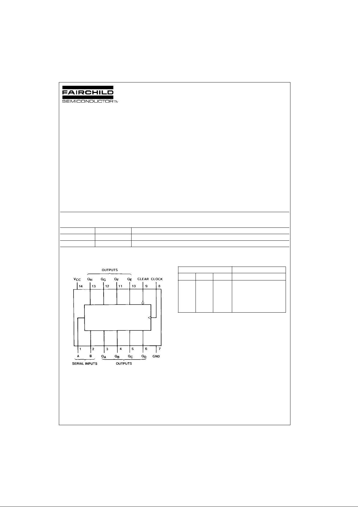
Connection Diagram Function Table
H = HIGH Level (steady state)
L = LOW Level (steady state)
X = Don't Care (any input, including transitions)
↑ = Transition from LOW-to-HIGH level
Q
A0
, QB0, QH0 = The level of QA, QB, or QH, respectively, before the
indicated steady-s t at e input conditions we re es t ablished.
Q
An
, QGn = The level of QA or QG before the most recent ↑ transition of the
clock; indicates a one-bit shift.
Order Number Package Number Package Description
DM74LS164M M14A 14-Lead Small Outline Integrated Circuit (SOIC), JEDEC MS-120, 0.150 Narrow
DM74LS164N N14A 14-Lead Plastic Dual-In-Line Package (PDIP), JEDEC MS-001, 0.300 Wide
Inputs Outputs
Clear Clock A B
Q
AQB
...
Q
H
LXXXLL...L
HLXXQ
A0QB0
... Q
H0
H ↑ HHHQAn... Q
Gn
H ↑ LX L QAn... Q
Gn
H ↑ XL L QAn... Q
Gn
www.fairchildsemi.com 2
DM74LS164
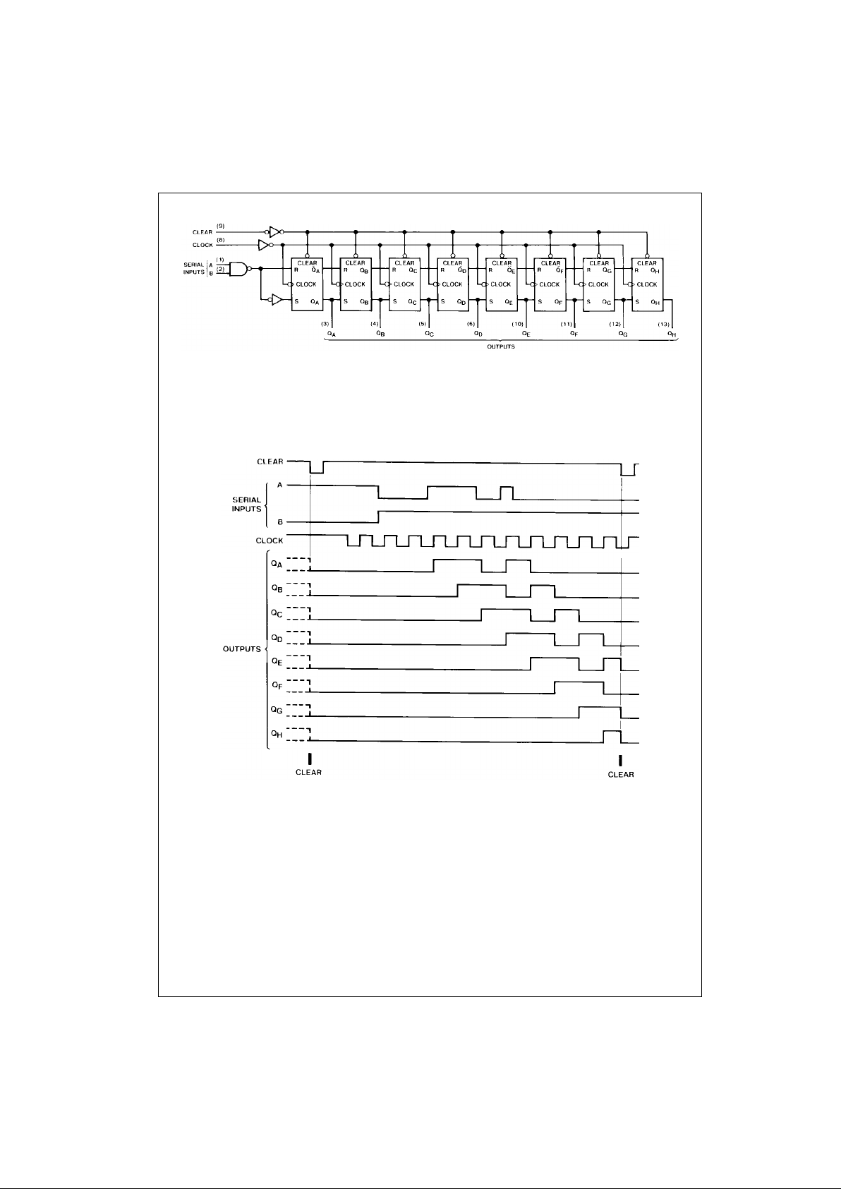
Logic Diagram
Timing Diagram

3 www.fairchildsemi.com
DM74LS164
Absolute Maximum Ratings(Note 1)
Note 1: The “Absolute Maximum Ratings ” are those val ues beyond w hich
the safety of the device cannot be guaranteed. The device should not be
operated at these limits. The parametric values defined in the Electrical
Characteristics tables are not guaranteed at the absolute maximum ratings.
The “Recommended Operating Conditio ns ” t ables will define the conditions
for actual device operation.
Recommended Operating Conditions
Note 2: TA = 25°C and VCC = 5V.
Electrical Characteristics
over recommended operating free air temperature range (unless otherwise noted)
Note 3: All typicals are at VCC = 5V, TA = 25°C.
Note 4: Not more than one output should be shorted at a time, and the duration should not exceed one second.
Note 5: I
CC
is measured with al l ou tputs OPE N, th e S ERIAL in put g round ed , the C LOC K in put a t 2. 4V, and a momen tary g rou nd, th en 4 .5V, applied to the
CLEAR input.
Switching Characteristics
at VCC = 5V and TA = 25°C
Supply Voltage 7V
Input Voltage 7V
Operating Free Air Temperature Range 0°C to +70°C
Storage Temperature Range −65°C to +150°C
Symbol Parameter Min Nom Max Units
V
CC
Supply Voltage 4.75 5 5.25 V
V
IH
HIGH Level Input Voltage 2 V
V
IL
LOW Level Input Voltage 0.8 V
I
OH
HIGH Level Output Current −0.4 mA
I
OL
LOW Level Output Current 8 mA
f
CLK
Clock Frequency (Note 2) 0 25 MHz
t
W
Pulse Width Clock 20
ns
(Note 2) Clear 20
t
SU
Data Setup Time (Note 2) 17 ns
t
H
Data Hold Time (Note 2) 5 ns
t
REL
Clear Release Time (Note 2) 30 ns
T
A
Free Air Operating Temperature 0 70 °C
Symbol Parameter Conditions Min
Typ
(Note 3)
Max Units
V
I
Input Clamp Voltage VCC = Min, II = −18 mA −1.5 V
V
OH
HIGH Level VCC = Min, IOH = Max
2.7 3.4 V
Output Voltage VIL = Max, VIH = Min
V
OL
LOW Level VCC = Min, IOL = Max
0.35 0.5
Output Voltage VIL = Max, VIH = Min V
IOL = 4 mA, VCC = Min 0.25 0.4
I
I
Input Current @ Max Input Voltage VCC = Max, VI = 7V 0.1 mA
I
IH
HIGH Level Input Current VCC = Max, VI = 2.7V 20 µA
I
IL
LOW Level Input Current VCC = Max, VI = 0.4V −0.4 mA
I
OS
Short Circuit Output Current VCC = Max (Note 4) −20 −100 mA
I
CC
Supply Current VCC = Max (Note 5) 16 27 mA
From (Input)
RL = 2 kΩ
Symbol Parameter To (Output)
CL = 15 pF CL = 50 pF
Units
MinMaxMinMax
f
MAX
Maximum Clock Frequency 25 M Hz
t
PLH
Propagation Delay Time
Clock to Output 27 30 ns
LOW-to-HIGH Level Output
t
PHL
Propagation Delay Time
Clock to Output 32 40 ns
HIGH-to-LOW Level Output
t
PHL
Propagation Delay Time
Clear to Output 36 45 ns
HIGH-to-LOW Level Output

www.fairchildsemi.com 4
DM74LS164
Physical Dimensions inches (millimeters) unless otherwise noted
14-Lead Small Outline Integrated Circuit (SOIC), JEDEC MS-120, 0.150 Narrow
Package Number M14A

5 www.fairchildsemi.com
DM74LS164 8-Bit Serial In/Parallel Out Shift Register
Physical Dimensions inches (millimeters) unless otherwise noted (Continued)
14-Lead Plastic Dual-In-Line Package (PDIP), JEDEC MS-001, 0.300 Wide
Package Number N14A
Fairchild does not assume any responsibility for use of any circu itry described, no circuit patent license s are implied and
Fairchild reserves the right at any time without notice to change said circuitry and specifications.
LIFE SUPPORT POLICY
FAIRCHILD’S PRODUCTS ARE NOT AUTHORIZED FOR USE AS CRITICAL COMPONENTS IN LIFE SUPPORT
DEVICES OR SYSTEMS WITHOUT THE EXPRESS WRITTEN APPROVAL OF THE PRESIDENT OF FAIRCHILD
SEMICONDUCTOR CORPORATION. As used herein:
1. Life support devices or systems are devices or systems
which, (a) are intended for surgical implant into the
body, or (b) support or sustain life, and (c) whose failure
to perform when properly used in accordance with
instructions for use provided i n the labe li ng, can be re asonably expected to result in a significant injury to the
user.
2. A critical compo nent in any com ponen t of a life s uppor t
device or system whose failu re to perform can b e reasonably expected to c ause th e fa i lure of the li fe s upp or t
device or system, or to affect its safety or effectiveness.
www.fairchildsemi.com
 Loading...