

Page 1
DM74LS161A • DM74LS163A
Synchronous 4-Bit Binary Counters
DM74LS161A • DM74LS163A Synchronous 4-Bit Binary Counters
August 1986
Revised April 2000
General Description
These synchronous, pres ettable counters fe ature an internal carry look-ahead for a ppli ca tion i n high -sp eed co unting
designs. The DM74LS161A and DM74LS163A are 4-bit
binary counters. The carry output is decoded by means of
a NOR gate, thus preventing spikes during the normal
counting mode of operation. Synchronous operation is provided by having all flip-flops clocked simultaneously so that
the outputs change coincident with each other when so
instructed by the count-enabl e inputs and internal gating.
This mode of operation eliminates the output counting
spikes which are normall y associated with asynchronous
(ripple clock) counters. A buffer ed clock input triggers t he
four flip-flops on the rising (positive-going) edge of the
clock input waveform.
These counters are fully programmable; that is, the outputs
may be preset to either level. As presetting is synchronous,
setting up a low level at the load in pu t disab l es th e co unt er
and causes the outputs to a gree with the setup dat a after
the next clock pulse, re gardl ess of the le vels o f the e nable
input. The clear function for the DM74LS161A is asynchronous; and a low level at the clear input se ts all four of t he
flip-flop outputs LOW, regardless of the levels of clock,
load, or enable inputs. The clear function for the
DM74LS163A is synchro nous; and a low leve l at the cl ear
inputs sets all four of the flip-flo p outputs LOW after the
next clock pulse, regardless of the levels of the enable
inputs. This synchronou s clear allows the count length to
be modified easily, as decoding the maximum count
desired can be accomplished with one external NAND
gate. The gate outpu t is connected to the clear input to
synchronously clear the counter to all low outputs.
The carry look-ahead circuitry provides for cascading
counters for n-bit synchro nous applications without additional gating. Instrumental in accomplishing this function
are two count-enable inputs and a ripple carry output.
Both count-enable inputs (P and T) must be HIGH to count,
and input T is fed forward to e nab l e th e rip ple ca rr y output.
The ripple carry output thus enabled will produce a highlevel output pulse w ith a duration approxim ately equal to
the high-level portion of the Q
flow ripple carry pu lse can be used to enabl e successive
cascaded stages. HIGH-to-LOW level transitions at the
enable P or T in puts may occur, regardless of the logic
level of the clock.
These counters fe ature a fully independent clock ci rcuit.
Changes made to control inputs (enable P or T or load) that
will modify the operating mode have no effect until clocking
occurs. The function of the cou nter (whether en abled, disabled, loading, or counti ng) will be dictated solely by the
conditions meeting the stable set-up and hold times.
output. This high-level over-
A
Features
■ Synchronously programmable
■ Internal look-ahead for fast counting
■ Carry output for n-bit cascading
■ Synchronous counting
■ Load control line
■ Diode-clamped inputs
■ Typical propagation time, clock to Q output 14 ns
■ Typical clock frequency 32 MHz
■ Typical power d issipation 93 mW
Ordering Code:
Order Number Package Number Package Description
DM74LS161AM M16A 16-Lead Small Outline Integrated Circuit (SOIC), JEDEC MS-012, 0.150 Narrow
DM74LS161AN N16E 16-Lead Plastic Dual-In-Line Package (PDIP), JEDEC MS-001, 0.300 Wide
DM74LS163AM M16A 16-Lead Small Outline Integrated Circuit (SOIC), JEDEC MS-012, 0.150 Narrow
DM74LS163AN N16E 16-Lead Plastic Dual-In-Line Package (PDIP), JEDEC MS-001, 0.300 Wide
Devices also availab le in Tape and Reel. Specify by appending th e s uffix let t er “X” to the ordering cod e.
© 2000 Fairchild Semiconductor Corporation DS006397 www.fairchildsemi.com
Page 2
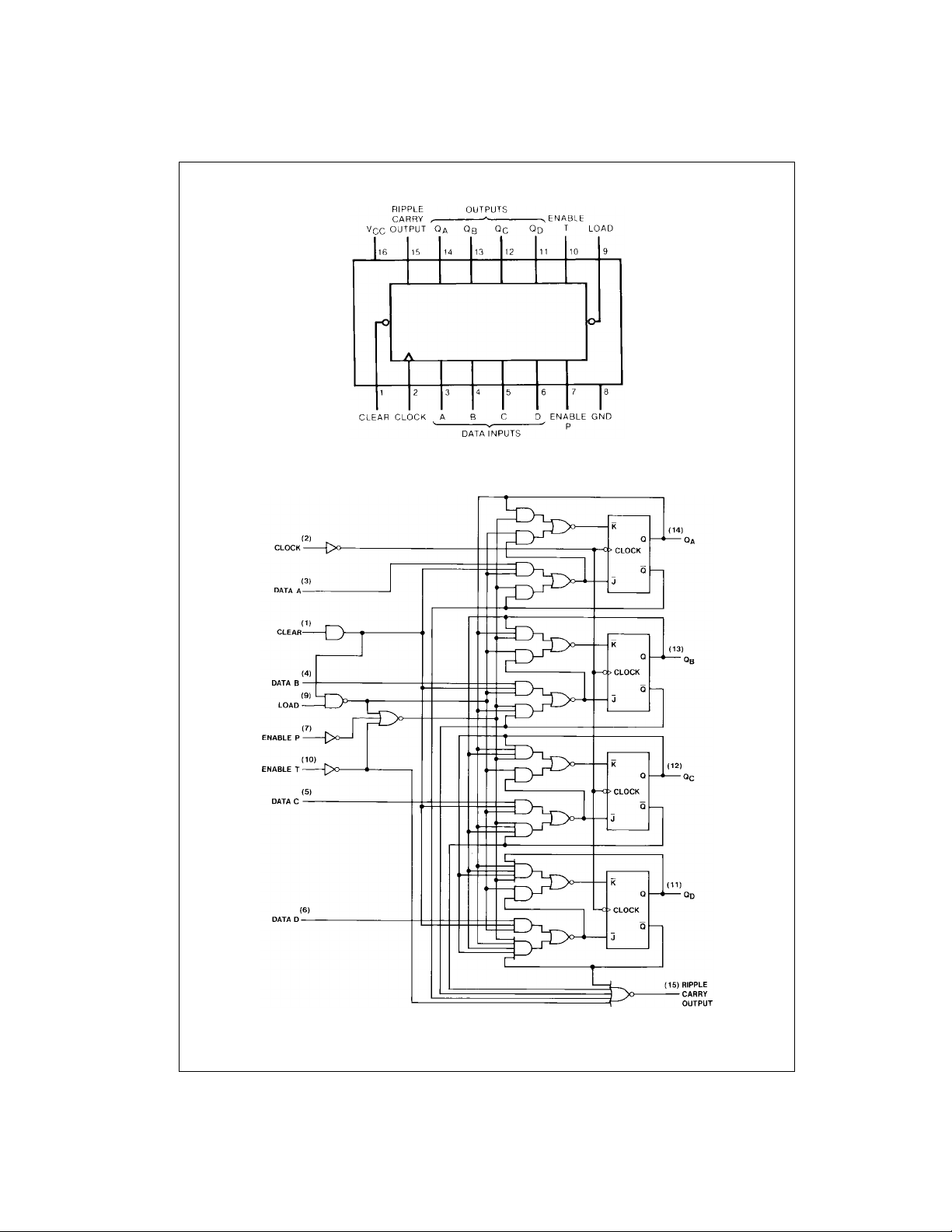
Connection Diagram
DM74LS161A • DM74LS163A
Logic Diagram
DM74LS163A
The DM74LS161A is similar, however, the clear buffer is conn ec t ed directly to the flip-flo ps .
www.fairchildsemi.com 2
Page 3
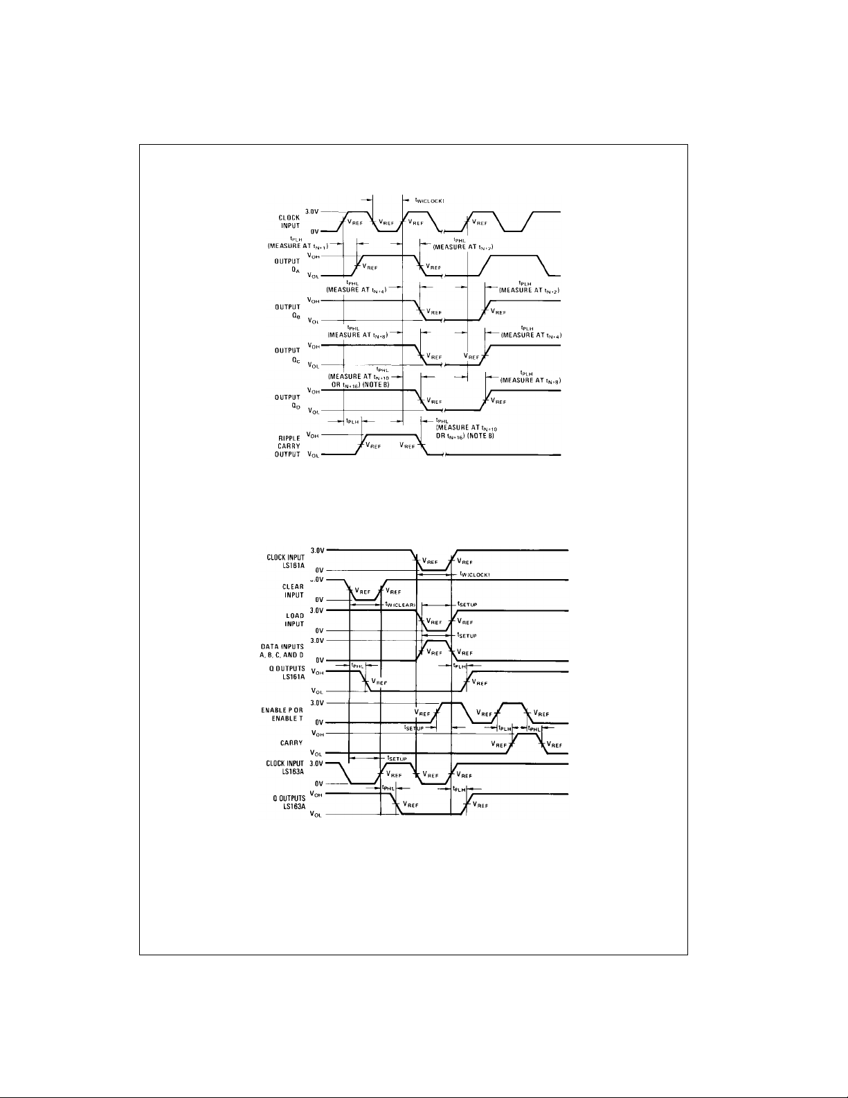
Parameter Measurement Information
Switching Time Waveforms
The input pulses are supplied by generators having the following c haracteristics:
PRR ≤ 1 MHz, duty cycle ≤ 50%, Z
Vary PRR to measure f
Outputs Q
D
V
= 1.5V.
REF
MAX
and carry are tested at t
.
≈ 50Ω, tR ≤ 10 ns, tF ≤ 10 ns.
OUT
where tN is the bit time when all o ut puts are LOW.
N+16
Switching Time Waveforms
DM74LS161A • DM74LS163A
The input pulses are supplied by generators having the following ch aracteristics:
PRR ≤ 1 MHz, duty cycle ≤ 50%, Z
Enable P and enable T s et up times are measured at t
= 1.3V.
V
REF
≈ 50Ω, tR ≤ 6 ns, tF ≤ 6 ns. Vary PRR to measure f
OUT
N+0
.
.
MAX
3 www.fairchildsemi.com
Page 4
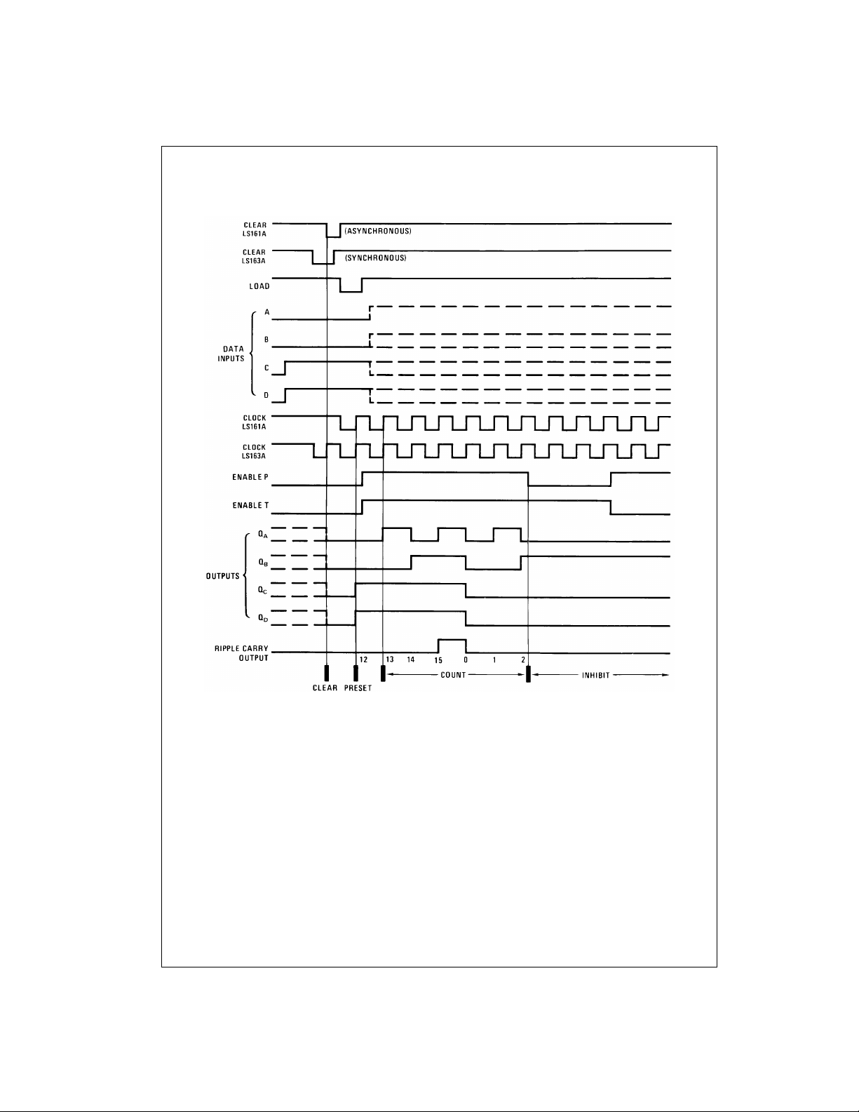
Timing Diagram
DM74LS161A • DM74LS163A
LS161A, LS163A Synchronous Binary Counters
Typical Clear, Preset, Count an d Inhibit Sequences
Sequence:
(1) Clear outputs to zero
(2) Preset to bina ry twelve
(3) Count to thirteen, fourteen, fifteen, zero, one, and two
(4) Inhibit
www.fairchildsemi.com 4
Page 5
Absolute Maximum Ratings(Note 1)
Supply Voltage 7V
Input Voltage 7V
Operating Free Air Temperature Range 0°C to +70°C
Storage Temperature Range −65°C to +150°C
Note 1: The “Absolute M aximu m R atin gs” are t hose valu es b eyo nd w hich
the safety of the device cannot be guaranteed. The device should not be
operated at these limits. The parametric values defined in the Electrical
Characteristics tables are not guaranteed at the absolute maximum ratings.
The “Recommend ed O peratin g Cond itions” t able w ill defin e the condit ions
for actual device operation.
DM74LS161A Recommended Operating Conditions
Symbol Parameter Min Nom Max Units
V
CC
V
IH
V
IL
I
OH
I
OL
f
CLK
t
W
t
SU
t
H
t
REL
T
A
Note 2: CL = 15 pF, RL = 2 kΩ, TA = 25°C and VCC = 5.5V.
Note 3: C
Supply Voltage 4.75 5 5.25 V
HIGH Level Input Voltage 2 V
LOW Level Input Voltage 0.8 V
HIGH Level Output Current −0.4 mA
LOW Level Output Current 8 mA
Clock Frequency (Note 2) 0 25 MHz
Clock Frequency (Note 3) 0 20 MHz
Pulse Width Clock 20 6
(Note 2) Clear 20 9
Pulse Width Clock 25
(Note 3) Clear 25
Setup Time Data 20 8
(Note 2) Enable P 25 17 ns
Load 25 15
Setup Time Data 20
(Note 3) Enable P 30 ns
Load 30
Hold Time Data 0 −3
(Note 2) Others 0 −3
Hold Time Data 5
(Note 3) Others 5
Clear Rele ase Time (Note 2) 20 ns
Clear Rele ase Time (Note 3) 25 ns
Free Air Operating Temperature 0 70 °C
= 50 pF, RL = 2 kΩ, TA = 25°C and VCC = 5.5V.
L
DM74LS161A • DM74LS163A
ns
ns
ns
ns
5 www.fairchildsemi.com
Page 6
DM74LS161A Electrical Characteristics
over recommended operating free air temperature range (unless otherwise noted)
Symbol Parameter Conditions Min
V
I
V
OH
V
OL
I
I
DM74LS161A • DM74LS163A
I
IH
I
IL
I
OS
I
CCH
I
CCL
Note 4: All typicals are at VCC = 5V, TA = 25°C.
Note 5: Not more than one output should be shorted at a time, and the duration should not exceed one second.
Note 6: I
Note 7: I
Input Clamp Voltage VCC = Min, II = −18 mA −1.5 V
HIGH Level VCC = Min, IOH = Max
Output Voltage VIL = Max, VIH = Min
LOW Level VCC = Min, IOL = Max
Output Voltage VIL = Max, VIH = Min V
IOL = 4 mA, VCC = Min 0.25 0.4
Input Current @ Max VCC = Max Enable T 0.2
Input Voltage VI = 7V Clock 0.2
Load 0.2
Others 0.1
HIGH Level VCC = Max Enable T 40
Input Current VI = 2.7V Clock 40
Load 40
Others 20
LOW Level VCC = Max Enable T −0.8
Input Current VI = 0.4V Clock −0.8
Load −0.8
Others −0.4
Short Circuit Output Current VCC = Max (Note 5) −20 −100 mA
Supply Current with Outputs HIGH VCC = Max (Note 6) 18 31 mA
Supply Current with Outputs LOW VCC = Max (Note 7) 19 32 mA
is measured with the load HIGH, then again with the load LOW, with all other input s H I GH and all outputs OPEN.
CCH
is measured with the cl oc k input HIGH, then again w it h t he clock input LOW, with all other inputs LOW and all output s OPEN.
CCL
Typ
(Note 4)
Max Units
2.7 3.4 V
0.35 0.5
mA
µA
mA
DM74LS161A Switching Characteristics
at VCC = 5V and TA = 25°C
Symbol Parameter To (Output) CL = 15 pF CL = 50 pF Uni ts
f
t
MAX
PLH
Maximum Clock Frequency 25 20 MHz
Propagation Delay Time Clock to
LOW-to-HIGH Level Output Ripple Carry
t
PHL
Propagation Delay Time Clock to
HIGH-to-LOW Level Output Ripple Carry
t
PLH
Propagation Delay Time Clock to Any Q
LOW-to-HIGH Level Output (Load HIGH)
t
PHL
Propagation Delay Time Clock to Any Q
HIGH-to-LOW Level Output (Load HIGH)
t
PLH
Propagation Delay Time Clock to Any Q
LOW-to-HIGH Level Output (Load LOW)
t
PHL
Propagation Delay Time Clock to Any Q
HIGH-to-LOW Level Output (Load LOW)
t
PLH
Propagation Delay Time Enable T to
LOW-to-HIGH Level Output Ripple Carry
t
PHL
Propagation Delay Time Enable T to
HIGH-to-LOW Level Output Ripple Carry
t
PHL
Propagation Delay Time Clear to
HIGH-to-LOW Level Output Any Q
www.fairchildsemi.com 6
From (Input) RL = 2 kΩ
Min Max Min Max
25 30 ns
30 38 ns
22 27 ns
27 38 ns
24 30 ns
27 38 ns
14 27 ns
15 27 ns
28 45 ns
Page 7
DM74LS163A Recommended Operating Conditions
Symbol Parameter Min Nom Max Units
V
CC
V
IH
V
IL
I
OH
I
OL
f
CLK
Supply Voltage 4.75 5 5.25 V
HIGH Level Input Voltage 2 V
LOW Level Input Voltage 0.8 V
HIGH Level Output Current −0.4 mA
LOW Level Output Current 8 mA
Clock Frequency (Note 8) 0 25 MHz
Clock Frequency (Note 9) 0 20 MHz
t
W
Pulse Width Clock 20 6
(Note 8) Clear 20 9
Pulse Width Clock 25
(Note 9) Clear 25
t
SU
Setup Time Data 20 8
(Note 8) Enable P 25 17 ns
Load 25 15
Setup Time Data 20
(Note 9) Enable P 30 ns
Load 30
t
H
Hold Time Data 0 −3
(Note 8) Others 0 −3
Hold Time Data 5
(Note 9) Others 5
t
REL
Clear Release Time (Note 8) 20 ns
Clear Release Time (Note 9) 25 ns
T
A
Note 8: CL = 15 pF, RL = 2 kΩ, TA = 25°C and VCC = 5V.
Note 9: C
Free Air Operating Temperature 0 70 °C
= 50 pF, RL = 2 kΩ, TA = 25°C and VCC = 5V.
L
DM74LS163A Electrical Characteristics
over recommended operating free air temperature range (unless otherwise noted)
Symbol Parameter Conditions Min
V
I
V
OH
Input Clamp Voltage VCC = Min, II = −18 mA −1.5 V
HIGH Level VCC = Min, IOH = Max
Output Voltage VIL = Max, VIH = Min
V
OL
LOW Level VCC = Min, IOL = Max
Output Voltage VIL = Max, VIH = Min V
IOL = 4 mA, VCC = Min 0.25 0.4
I
I
Input Current @ Max VCC = Max Enable T 0.2
Input Voltage VI = 7V Clock, Clear 0.2
Load 0.2
Others 0.1
I
IH
HIGH Level VCC = Max Enable T 40
Input Current VI = 2.7V Load 40
Clock, Clear 40
Others 20
I
IL
LOW Level VCC = Max Enable T −0.8
Input Current VI = 0.4V Clock, Clear −0.8
Load −0.8
Others −0.4
I
OS
I
CCH
I
CCL
Note 10: All typicals ar e at VCC = 5V, TA = 25°C.
Note 11: Not more than one output should be shorted at a t im e, and the duration shou ld not exceed one second.
Note 12: I
Note 13: I
Short Circuit Output Current VCC = Max (Note 11) −20 −100 mA
Supply Current with Outputs HIGH VCC = Max (Note 12) 18 31 mA
Supply Current with Outputs LOW VCC = Max (Note 13) 18 32 mA
is measured with the lo ad HIGH, then again wit h t he load LOW, with all other inputs HIGH and all outputs OPEN.
CCH
is measured with the clock input HIGH, then again with the clock input LOW, with all other inputs LOW and all outputs OPEN.
CCL
2.7 3.4 V
Typ
(Note 10)
0.35 0.5
Max Units
DM74LS161A • DM74LS163A
ns
ns
ns
ns
mA
µA
mA
7 www.fairchildsemi.com
Page 8
DM74LS163A Switching Characteristics
at VCC = 5V and TA = 25°C
Symbol Parameter To (Output)
f
t
MAX
PLH
Maximum Clock Frequency 25 20 MHz
Propagation Delay Time Clock to
LOW-to-HIGH Level Output Ripple Carry
t
PHL
Propagation Delay Time Clock to
HIGH-to-LOW Level Output Ripple Carry
t
PLH
Propagation Delay Time Clock to Any Q
LOW-to-HIGH Level Output (Load HIGH)
DM74LS161A • DM74LS163A
t
PHL
t
PLH
Propagation Delay Time Clock to Any Q
HIGH-to-LOW Level Output (Load HIGH)
Propagation Delay Time Clock to Any Q
LOW-to-HIGH Level Output (Load LOW)
t
PHL
Propagation Delay Time Clock to Any Q
HIGH-to-LOW Level Output (Load LOW)
t
PLH
Propagation Delay Time Enable T to
LOW-to-HIGH Level Output Ripple Carry
t
PHL
Propagation Delay Time Enable T to
HIGH-to-LOW Level Output Ripple Carry
t
PHL
Propagation Delay Time Clear to Any Q
HIGH-to-LOW Level Output (Note 14)
Note 14: The propagation delay clear to output is measured from t he clock input transition.
From (Input)
RL = 2 kΩ
CL = 15 pF CL = 50 pF
Min Max Min Max
25 30 ns
30 38 ns
22 27 ns
27 38 ns
24 30 ns
27 38 ns
14 27 ns
15 27 ns
28 45 ns
Units
www.fairchildsemi.com 8
Page 9
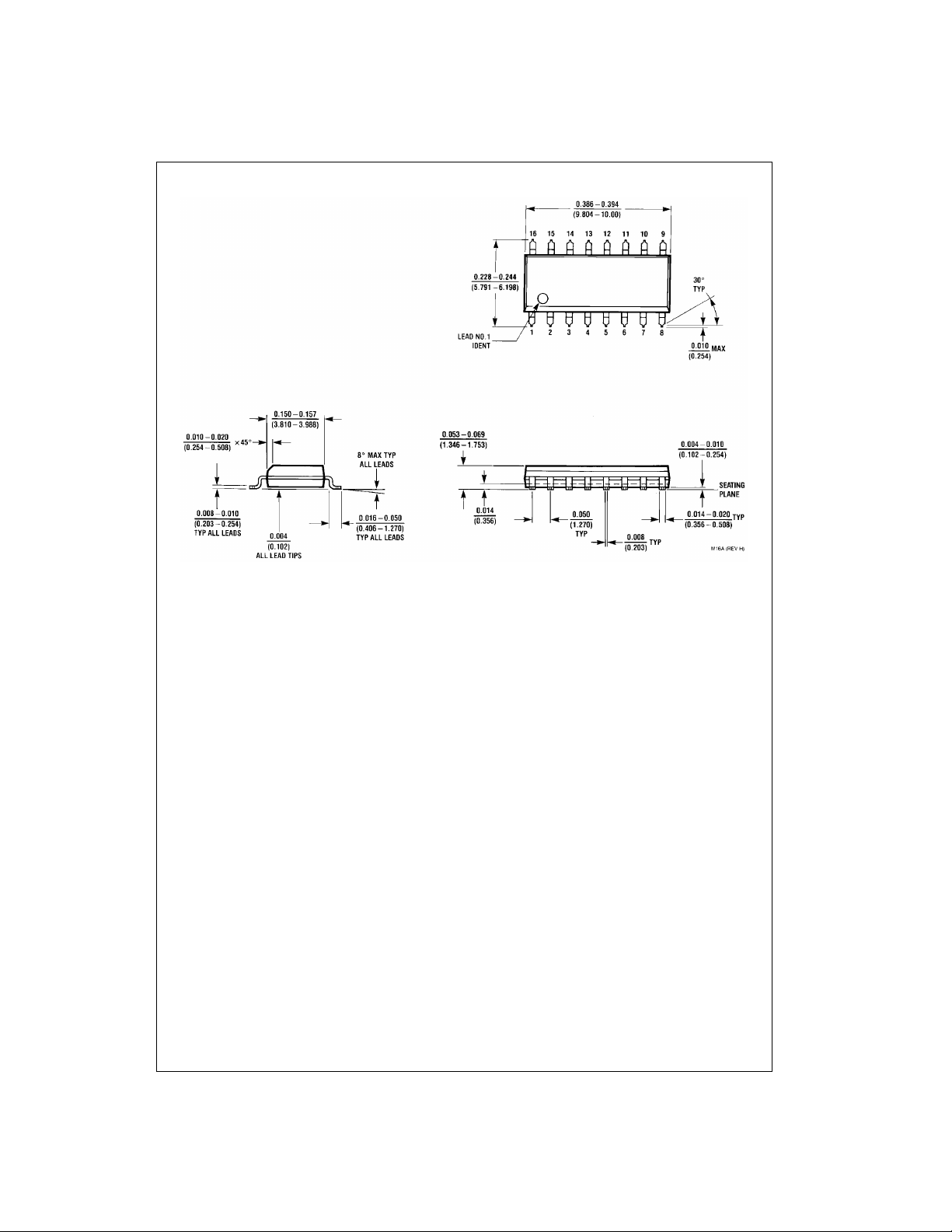
Physical Dimensions inches (millimeters) unless otherwise noted
DM74LS161A • DM74LS163A
16-Lead Small Outline Integrated Circuit (SOIC), JEDEC MS-012, 0.150 Narrow
Package Number M16A
9 www.fairchildsemi.com
Page 10
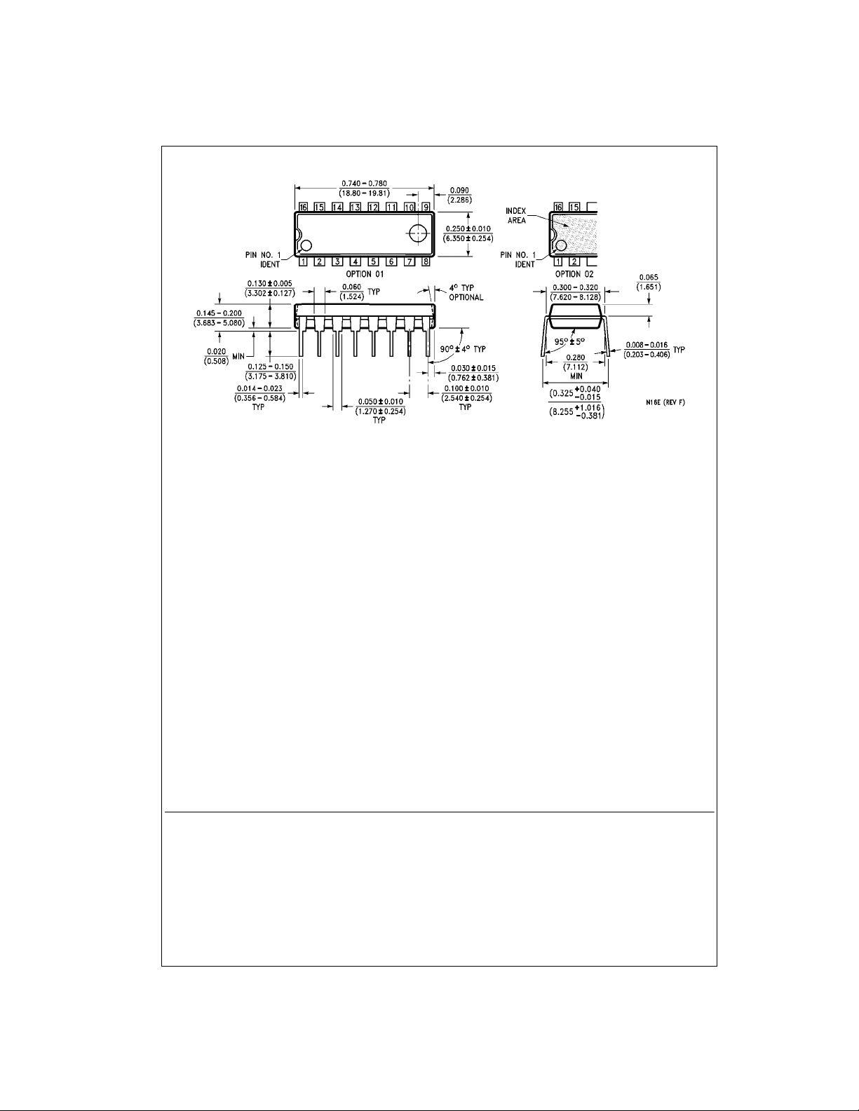
Physical Dimensions inches (millimeters) unless otherwise noted (Continued)
16-Lead Plastic Dual-In-Line Package (PDIP), JEDEC MS-001, 0.300 Wide
Package Number N16E
DM74LS161A • DM74LS163A Synchronous 4-Bit Binary Counters
Fairchild does not assume any responsibility for us e of any circuitry described, no circuit patent licenses are implied and
Fairchild reserves the right at any time without notice to change said circuitry and specifications.
LIFE SUPPORT POLICY
FAIRCHILD’S PRODUCTS ARE NOT AUTHORIZED FOR USE AS CRITICAL COMPONENTS IN LIFE SUPPORT
DEVICES OR SYSTEMS WITHOUT THE EXPRESS WRITTEN APPROVAL OF THE PRESIDENT OF FAIRCHILD
SEMICONDUCTOR CORPORATION. As used herein:
1. Life support devices or systems are devices or syste ms
which, (a) are intended for surgical implant into the
body, or (b) support or sustain life, and (c) whose failure
to perform when properly used in accordance with
instructions for use provided in the labeling, can be reasonably expected to result in a significan t injury to the
user.
2. A critical component in any compon ent of a l ife supp ort
device or system whose failu re to perform can be reasonably expected to ca use the fa i lure of the li fe su pp ort
device or system, or to affect its safety or effectiveness.
www.fairchildsemi.com
www.fairchildsemi.com 10
 Loading...