

Page 1
© 2000 Fairchild Semiconductor Corporation DS006395 www.fairchildsemi.com
August 1986
Revised April 2000
DM74LS155 • DM74LS156 Dual 2-Line to 4-Line Decoders/Demultiplexers
DM74LS155 • DM74LS156
Dual 2-Line to 4-Line Decoders/Demultiplexers
General Description
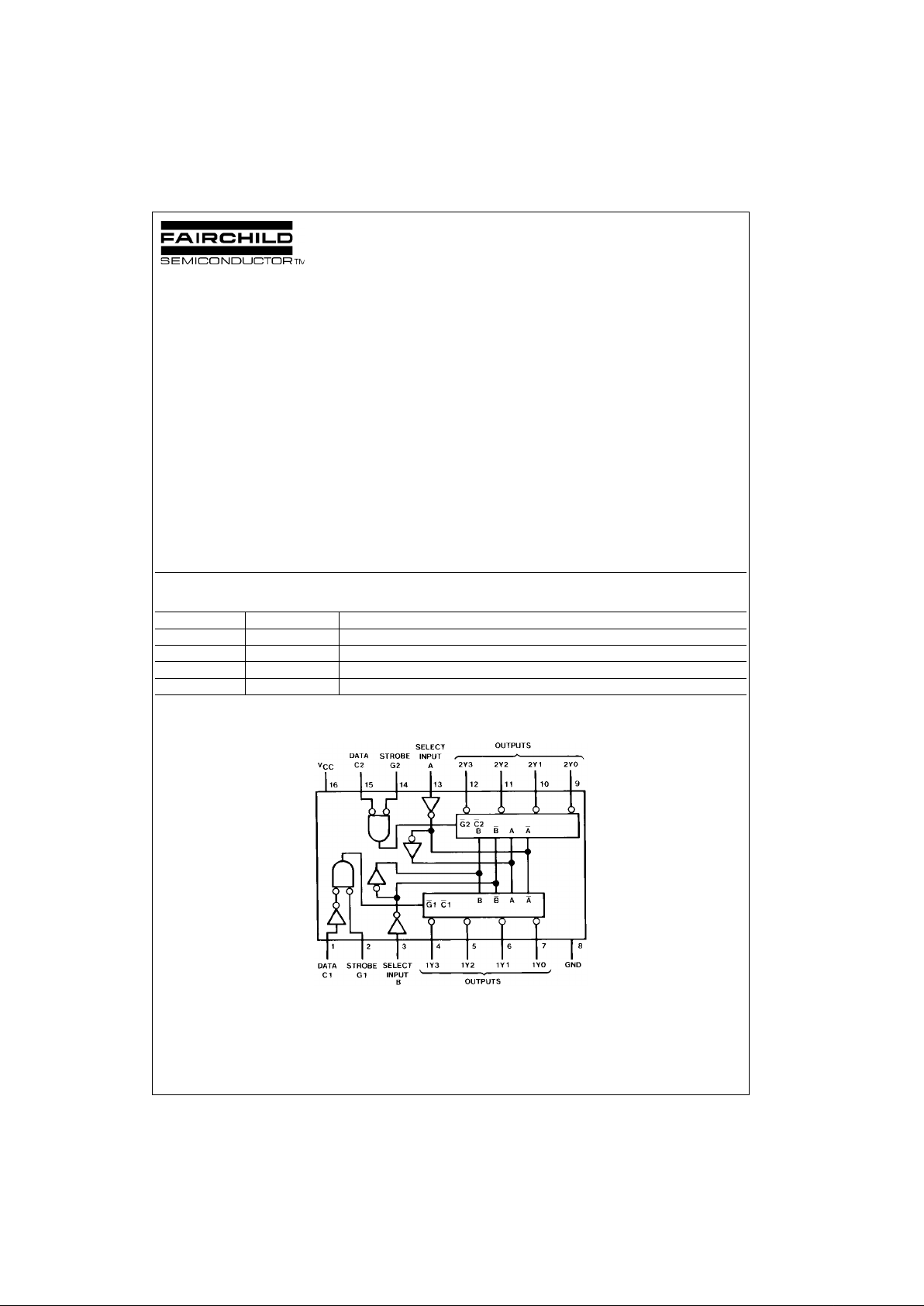
These TTL circuits feature dual 1-line-to-4-line demultiplexers with individual strobes and common binary-address
inputs in a single 16-pin package. W hen both sectio ns are
enabled by the strobes, the common address inputs
sequentially select and route ass ociated input data to the
appropriate output of each section . The individual strobes
permit activating or i nhibiting each of the 4-bit sections as
desired. Data applied to input C1 is inverted at its outputs
and data applied at C2 is true through its outputs. The
inverter following the C1 data input permits use as a 3-to-8line decoder, or 1-to-8-line demultiplexer, without external
gating. Input clamping diod es are provided on these circuits to minimize transmission-line effects and simplify system design.
Features
■ Applications:
Dual 2-to-4-line decoder
Dual 1-to-4-line demultiplexer
3-to-8-line decoder
1-to-8-line demultiplexer
■ Individual strobes simplify cascading for decoding or
demultiplexing larger words
■ Input clamping diodes simplify system design
■ Choice of outputs:
Totem-pole (DM74LS155)
Open-collector (DM74LS156)
Ordering Code:
Devices also availab le in Tape and Reel. Specify by appending th e s uffix let t er “X” to the ordering code.
Connection Diagram
Order Number Package Number Package Description
DM74LS155M M16A 16-Lead Small Outline Integrated Circuit (SOIC), JEDEC MS-012, 0.150 Narrow
DM74LS155N N16E 16-Lead Plastic Dual-In-Line Package (PDIP), JEDEC MS-001, 0.300 Wide
DM74LS156M M16A 16-Lead Small Outline Integrated Circuit (SOIC), JEDEC MS-012, 0.150 Narrow
DM74LS156N N16E 16-Lead Plastic Dual-In-Line Package (PDIP), JEDEC MS-001, 0.300 Wide
Page 2
www.fairchildsemi.com 2
DM74LS155 • DM74LS156
Function Tables
3-Line-to-8-Line Decoder or 1-Line-to-8-Line Demultiplexer
2-Line-to-4-Line Decoder or 1-Line-to-4-Line Demultiplexer
H = HIGH level
L = LOW level
X = don’t care
Note 1: C = inputs C1 and C2 connected together
Note 2: G = inputs G1 and G2 connected together
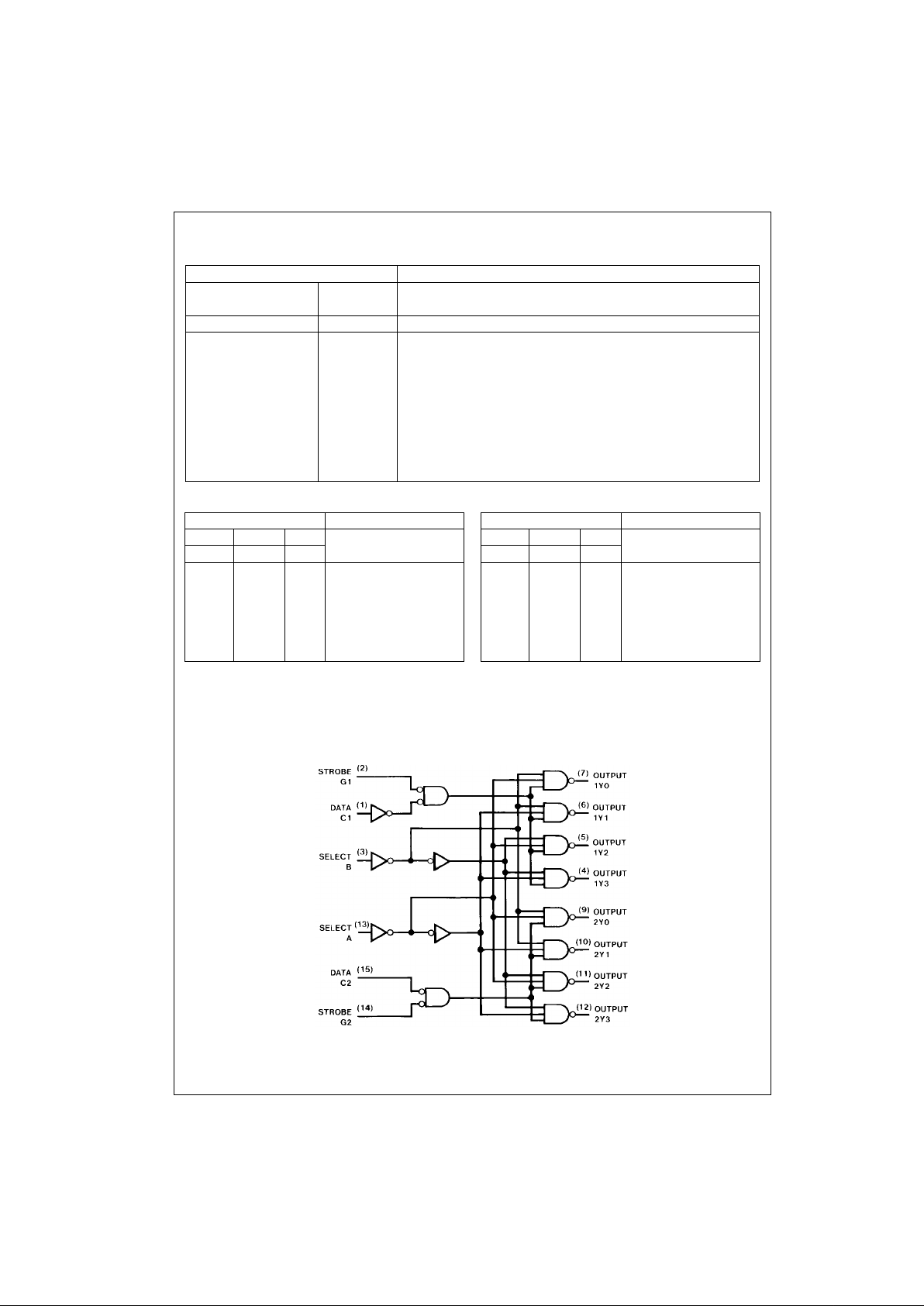
Logic Diagram
Inputs Outputs
Select
Strobe
(0) (1) (2) (3) (4) (5) (6) (7)
Or Data
C (Note 1) B A G (Note 2) 2Y0 2Y1 2Y2 2Y3 1Y0 1Y1 1Y2 1Y3
X XX H HHHHHHHH
L LL L LHHHHHHH
L LH L HLHHHHHH
L HL L HHLHHHHH
L HH L HHHLHHHH
H LL L HHHHLHHH
H LH L HHHHHLHH
H HL L HHHHHHLH
H HH L HHHHHHHL
Inputs Outputs
Select Strobe Data
1Y0 1Y1 1Y2 1Y3
BA G1 C1
XX H X HHHH
LL L H LHHH
LH L H H L H H
HL L H H H L H
HH L H H H H L
XX X L HHHH
Inputs Outputs
Select Strobe Data
2Y02Y12Y22Y3
BA G2 C2
XX H X HHHH
LL L L L H H H
LH L L H L H H
HL L L H H L H
HH L L H H H L
XX X H HHHH
Page 3

3 www.fairchildsemi.com
DM74LS155 • DM74LS156
Absolute Maximum Ratings(Note 3)
Note 3: The “Absolute Maximum Ratings ” are those val ues beyond w hich
the safety of the device cannot be guaranteed. The device should not be
operated at these limits. The parametric values defined in the Electrical
Characteristics tables are not guaranteed at the absolute maximum ratings.
The “Recommend ed O peratin g Cond itions” t able w ill defin e the condition s
for actual device operation.
DM74LS155 Recommended Operating Conditions
DM74LS155 Electrical Characteristics
over recommended operating free air temperature range (unless otherwise noted)
Note 4: All typicals are at VCC = 5V, TA = 25° C.
Note 5: Not more than one output should be shorted at a time, and the duration should not exceed one second.
Note 6: I
CC
is measured with all outputs OPEN, A,B, and C1 inputs at 4.5V, and C2, G1, and G2 inputs GROUNDED.
DM74LS155 Switching Characteristics
at VCC = 5V and TA = 25°C
Supply Voltage 7V
Input Voltage 7V
Operating Free Air Temperature Range 0°C to +70°C
Storage Temperature Range −65°C to +150°C
Symbol Parameter Min Nom Max Units
V
CC
Supply Voltage 4.75 5 5.25 V
V
IH
HIGH Level Input Voltage 2 V
V
IL
LOW Level Input Voltage 0.8 V
V
OH
HIGH Level Output Current −0.4 mA
I
OL
LOW Level Output Current 8 mA
T
A
Free Air Operating Temperature 0 70 °C
Symbol Parameter Conditions Min
Typ
Max Units
(Note 4)
V
I
Input Clamp Voltage VCC = Min, II = −18 mA −1.5 V
V
OH
HIGH Level VCC = Min, IOH = Max
2.7 3.4 V
Output Voltage VIL = Max, VIH = Min
V
OL
LOW Level VCC = Min, IOL = Max
0.35 0.5
Output Voltage VIL = Max, VIH = Min V
IOL = 4 mA, VCC = Min 0.25 0.4
I
I
Input Current @ Max Input Voltage VCC = Max, VI = 7V 0.1 mA
I
IH
HIGH Level Input Current VCC = Max, VI = 2.7V 20 µA
I
IL
LOW Level Input Current VCC = Max, VI = 0.4V −0.36 mA
I
OS
Short Circuit Output Current VCC = Max (Note 5) −20 −100 mA
I
CC
Supply Current VCC = Max (Note 6) 6.1 10 mA
From (Input)
RL = 2 kΩ
Symbol Parameter
To (Output)
CL = 15 pF CL = 50 pF Units
Min Max Min Max
t
PLH
Propagation Delay Time A, B, C2, G1
18 22 ns
LOW-to-HIGH Level Output or G2 to Y
t
PHL
Propagation Delay Time A, B, C2, G1
27 35 ns
HIGH-to-LOW Level Output or G2 to Y
t
PLH
Propagation Delay Time A or B
18 24 ns
LOW-to-HIGH Level Output to Y
t
PHL
Propagation Delay Time A or B
27 35 ns
HIGH-to-LOW Level Output to Y
t
PLH
Propagation Delay Time C1
20 24 ns
LOW-to-HIGH Level Output to Y
t
PHL
Propagation Delay Time C1
27 35 ns
HIGH-to-LOW Level Output to Y
Page 4

www.fairchildsemi.com 4
DM74LS155 • DM74LS156
DM74LS156 Recommended Operating Conditions
DM74LS156 Electrical Characteristics
over recommended operating free air temperature range (unless otherwise noted)
Note 7: All typicals are at VCC = 5V, TA = 25° C.
Note 8: I
CC
is measured with all outputs OPEN, A, B, and C1 inputs at 4.5V, and C2, G1, and G2 GROUNDED.
DM74LS156 Switching Characteristics
at VCC = 5V and TA = 25°C
Symbol Parameter Min Nom Max Units
V
CC
Supply Voltage 4.75 5 5.25 V
V
IH
HIGH Level Input Voltage 2 V
V
IL
LOW Level Input Voltage 0.8 V
V
OH
HIGH Level Output Voltage 5.5 V
I
OL
LOW Level Output Current 8 mA
T
A
Free Air Operating Temperature 0 70 °C
Symbol Parameter Conditions Min
Typ
Max Units
(Note 7)
V
I
Input Clamp Voltage VCC = Min, II = −18 mA −1.5 V
I
CEX
HIGH Level VCC = Min, VO = 5.5V
100 µA
Output Current VIL = Max, VIH = Min
V
OL
LOW Level VCC = Min, IOL = Max
0.35 0.5
Output Voltage VIL = Max, VIH = Min V
IOL = 4 mA, VCC = Min 0.25 0.4
I
I
Input Current @ Max Input Voltage VCC = Max, VI = 7V 0.1 mA
I
IH
HIGH Level Input Current VCC = Max, VI = 2.7V 20 µA
I
IL
LOW Level Input Current VCC = Max, VI = 0.4V −0.36 mA
I
CC
Supply Current VCC = Max (Note 8) 6.1 10 mA
From (Input)
RL = 2 kΩ
Symbol Parameter To (Output)
CL = 15 pF CL = 50 pF
Units
Min Max Min Max
t
PLH
Propagation Delay Time A, B, C2, G1
28 53 ns
LOW-to-HIGH Level Output or G2 to Y
t
PHL
Propagation Delay Time A, B, C2, G1
33 43 ns
HIGH-to-LOW Level Output or G2 to Y
t
PLH
Propagation Delay Time A or B
28 53 ns
LOW-to-HIGH Level Output to Y
t
PHL
Propagation Delay Time A or B
33 43 ns
HIGH-to-LOW Level Output to Y
t
PLH
Propagation Delay Time C1
28 53 ns
LOW-to-HIGH Level Output to Y
t
PHL
Propagation Delay Time C1
34 43 ns
HIGH-to-LOW Level Output to Y
Page 5

5 www.fairchildsemi.com
DM74LS155 • DM74LS156
Physical Dimensions inches (millimeters) unless otherwise noted
16-Lead Small Outline Integrated Circuit (SOIC), JEDEC MS-012, 0.150 Narrow
Package Number M16A
Page 6

www.fairchildsemi.com 6
DM74LS155 • DM74LS156 Dual 2-Line to 4-Line Decoders/Demultiplexers
Physical Dimensions inches (millimeters) unless otherwise noted (Continued)
16-Lead Plastic Dual-In-Line Package (PDIP), JEDEC MS-001, 0.300 Wide
Package Number N16E
Fairchild does not assume any responsibility for use of any circuitry described, no circuit pate nt licenses are implied and
Fairchild reserves the right at any time without notice to change said circuitry and specifications.
LIFE SUPPORT POLICY
FAIRCHILD’S PRODUCTS ARE NOT AUTHORIZED FOR USE AS CRITICAL COMPONENTS IN LIFE SUPPORT
DEVICES OR SYSTEMS WITHOUT THE EXPRESS WRITTEN APPROVAL OF THE PRESIDENT OF FAIRCHILD
SEMICONDUCTOR CORPORATION. As used herein:
1. Life support devices or systems are devices or syste ms
which, (a) are intended for surgical implant into the
body, or (b) support or sustain life, and (c) whose failure
to perform when properly used in accordance with
instructions for use provided in the labeling, can be reasonably expected to result in a significant inju ry to the
user.
2. A critical component i n any compon ent of a lif e support
device or system whose failu re to perform can be reasonably expected to ca use the fa i lure of the life su pp ort
device or system, or to affect its safety or effectiveness.
www.fairchildsemi.com
 Loading...