

Datasheet DM74LS112AN, DM74LS112AMX, DM74LS112AM, DM74LS112ACW Datasheet (Fairchild Semiconductor)
Page 1
© 2000 Fairchild Semiconductor Corporation DS006382 www.fairchildsemi.com
August 1986
Revised March 2000
DM74LS112 A Dual Negative-Edge-Triggered Master-Slave J-K Flip-Flop with Preset, Clear, and Complementary
Outputs
DM74LS112A
Dual Negative-Edge-T riggered Master-Slave J-K Flip-Flop
with Preset, Clear, and Complementary Outputs
General Description
This device contains two indepe ndent negative-edge-triggered J-K flip-flops with complementary outputs. The J and
K data is processed by the flip-flop on the falling edge of
the clock pulse. The clock triggering occurs at a volta ge
level and is not directly re lated to the transition time of the
falling edge of the clock pulse. Data on the J and K inputs
may be changed w hile the clock is HIGH or LOW without
affecting the outputs as lo ng as the setup and hold times
are not violated. A low logic lev el on the preset or clear
inputs will set or reset the outputs regardless of the logic
levels of the other inputs.
Ordering Code:
Devices also availab le in Tape and Reel. Specify by appending th e s uffix let t er “X” to the ordering code.
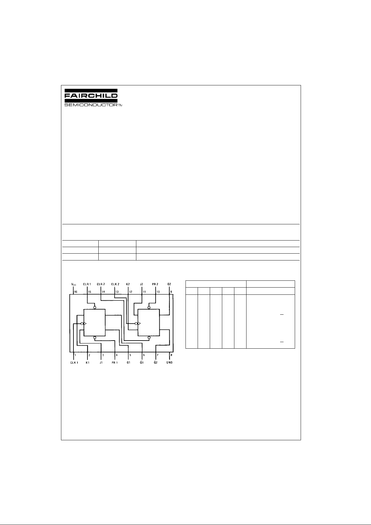
Connection Diagram Function Table
H = HIGH Logic Level
L = LOW Logic Level
X = Either LOW or HIGH Logic Level
↓ = Negative Going Edge of Pulse
Q
0
= Th e output logic level before the indicated input conditions were
established.
Toggle = Each output changes to the complement of its previous level on
each falling edge of th e c loc k pulse.
Note 1: This configuration is nonstable; that is, it will no t persist when
preset and/or clear inputs return to their inact iv e (H I GH) level.
Order Number Package Number Package Description
DM74KS112AM M16A 16-Lead Small Outline Integrated Circuit (SOIC), JEDEC MS-012, 0.150 Narrow
DM74LS112AN N16E 16-Lead Plastic Dual-In-Line Package (PDIP), JEDEC MS-001, 0.300 Wide
Inputs Outputs
PR CLR CLK J K Q Q
LHXXX H L
HLXXX L H
L L X X X H (Note 1) H (Note 1)
HH↓ LL Q
0
Q
0
HH↓ HL H L
HH↓ LH L H
HH↓ HH Toggle
HHHXX Q
0
Q
0
Page 2
www.fairchildsemi.com 2
DM74LS112A
Absolute Maximum Ratings(Note 2)
Note 2: The “Absolute Maximum Ratin gs” are those v alues beyon d which
the safety of the dev ice cannot be guaranteed. T he device sh ould not be
operated at these limits. The parametric values defined in the Electrical
Characteristics tables are not guaranteed at the absolute maximum ratings.
The “Recommend ed O peratin g Cond itions” t able w ill defin e the co ndition s
for actual device operation.
Recommended Operating Conditions
Note 3: CL = 15 pF, RL = 2 kΩ, TA = 25°C and VCC = 5V.
Note 4: The symbol (↓) indicates the falling edge of the clock puls e is used for reference.
Note 5: C
L
= 50 pF, RL = 2 kΩ, TA = 25°C and VCC = 5V.
Supply Voltage 7V
Input Voltage 7V
Operating Free Air Temperature Range 0°C to +70°C
Storage Temperature Range −65°C to +150°C
Symbol Parameter Min Nom Max Units
V
CC
Supply Voltage 4.75 5 5.25 V
V
IH
HIGH Level Input Voltage 2 V
V
IL
LOW Level Input Voltage 0.8 V
I
OH
HIGH Level Output Current −0.4 mA
I
OL
LOW Level Output Current 8 mA
f
CLK
Clock Frequency (Note 3) 0 30 MHz
f
CLK
Clock Frequency (Note 5) 0 25 MHz
t
W
Pulse Width Clock HIGH 20
(Note 3) Preset LOW 25 ns
Clear LOW 25
t
W
Pulse Width Clock HIGH 25
(Note 5) Preset LOW 30 ns
Clear LOW 30
t
SU
Setup Time (Note 3)(Note 4) 20↓ ns
t
SU
Setup Time (Note 4)(Note 5) 25↓ ns
t
H
Hold Time (Note 3)(Note 4) 0↓ ns
t
H
Hold Time (Note 4)(Note 5) 5↓ ns
T
A
Free Air Operating Temperature 0 70 °C
Page 3

3 www.fairchildsemi.com
DM74LS112A
Electrical Characteristics
over recommended operating free air temperature range (unless otherwise noted)
Note 6: All typicals are at VCC = 5V, TA = 25°C.
Note 7: Not more than one out put sh ould be shorted at a time, and the duration sh ould not exceed one second. For dev ic es , with fe edback from the outputs,
where shorting the outputs to g r ound ma y ca use the outputs to change logic stat e an e qui vale nt te st may be performed where V
O
= 2.125V with the minimum
and maximum limits reduced by one half from t heir stated values. This is v ery us eful when using autom atic test equipment .
Note 8: With all outputs OPEN, I
CC
is measured with the Q and Q outputs HIGH in turn. At th e t im e of measurement the c lock is grounded.
Switching Characteristics
at VCC = 5V and TA = 25°C
Symbol Parameter Conditions Min
Typ
Max Units
(Note 6)
V
I
Input Clamp Voltage VCC = Min, II = −18 mA −1.5 V
V
OH
HIGH Level VCC = Min, IOH = Max
2.7 3.4 V
Output Voltage VIL = Max, VIH = Min
V
OL
LOW Level VCC = Min, IOL = Max
0.35 0.5
Output Voltage VIL = Max, VIH = Min V
IOL = 4 mA, VCC = Min 0.25 0.4
I
I
Input Current @ Max VCC = Max, VI = 7V J, K 0.1
Input Voltage Clear 0.3
mA
Preset 0.3
Clock 0.4
I
IH
HIGH Level Input Current VCC = Max, VI = 2.7V J, K 20
Clear 60
µA
Preset 60
Clock 80
IIL LOW Level Input Current VCC = Max, VI = 0.4V J, K −0.4
Clear −0.8
mA
Preset −0.8
Clock −0.8
I
OS
Short Circuit Output Current VCC = Max (Note 7) −20 −100 mA
I
CC
Supply Current VCC = Max (Note 8) 4 6 mA
From (Input) RL = 2 kΩ
Symbol Parameter
To (Output)
CL = 15 pF CL = 50 pF Units
Min Max Min Max
f
MAX
Maximum Clock Frequency 30 25 MHz
t
PLH
Propagation Delay Time
Preset to Q 20 24 ns
LOW-to-HIGH Level Output
t
PHL
Propagation Delay Time
Preset to Q 20 28 ns
HIGH-to-LOW Level Output
t
PLH
Propagation Delay Time
Clear to Q 20 24 ns
LOW-to-HIGH Level Output
t
PHL
Propagation Delay Time
Clear to Q 20 28 ns
HIGH-to-LOW Level Output
t
PLH
Propagation Delay Time
Clock to Q or Q 20 24 ns
LOW-to-HIGH Level Output
t
PHL
Propagation Delay Time
Clock to Q or Q 20 28 ns
HIGH-to-LOW Level Output
Page 4

www.fairchildsemi.com 4
DM74LS112A
Physical Dimensions inches (millimeters) unless otherwise noted
16-Lead Small Outline Integrated Circuit (SOIC), JEDEC MS-012, 0.150 Narrow
Package Number M16A
Page 5

5 www.fairchildsemi.com
DM74LS112 A Dual Negative-Edge-Triggered Master-Slave J-K Flip-Flop with Preset, Clear, and Complementary
Outputs
Physical Dimensions inches (millimeters) unless otherwise noted (Continued)
16-Lead Plastic Dual-In-Line Package (PDIP), JEDEC MS-001, 0.300 Wide
Package Number N16E
Fairchild does not assume any responsibility for use of any circu itry described, no circuit patent license s are implied and
Fairchild reserves the right at any time without notice to change said circuitry and specifications.
LIFE SUPPORT POLICY
FAIRCHILD’S PRODUCTS ARE NOT AUTHORIZED FOR USE AS CRITICAL COMPONENTS IN LIFE SUPPORT
DEVICES OR SYSTEMS WITHOUT THE EXPRESS WRITTEN APPROVAL OF THE PRESIDENT OF FAIRCHILD
SEMICONDUCTOR CORPORATION. As used herein:
1. Life support devices or systems are dev ic es or syste ms
which, (a) are intended for surgical implant into the
body, or (b) support or sustain life, and (c) whose failure
to perform when properly used in accordance with
instructions for use provided i n the labe li ng, can be re asonably expected to result in a significant injury to the
user.
2. A critical componen t in any com ponent o f a l ife supp ort
device or system whose failu re to perform can b e reasonably expected to c ause th e fa i lure of the li fe s upp or t
device or system, or to affect its safety or effectiveness.
www.fairchildsemi.com
 Loading...