

Page 1
August 1986
Revised March 2000
DM74LS10
Triple 3-Input NAND Gate
General Description
This device contains three independent gates each of
which performs the logic NAND function.
Ordering Code:
Order Number Package Number Package Description
DM74LS10M M14A 14-Lead Small Outline Integrated Circuit (SOIC), JEDEC MS-120, 0.150 Narrow
DM74LS10N N14A 14-Lead Plastic Dual-In-Line Package (PDIP), JEDEC MS-001, 0.300 Wide
Devices also availab le in Tape and Reel. Specify by appending th e s uffix let t er “X” to the ordering cod e.
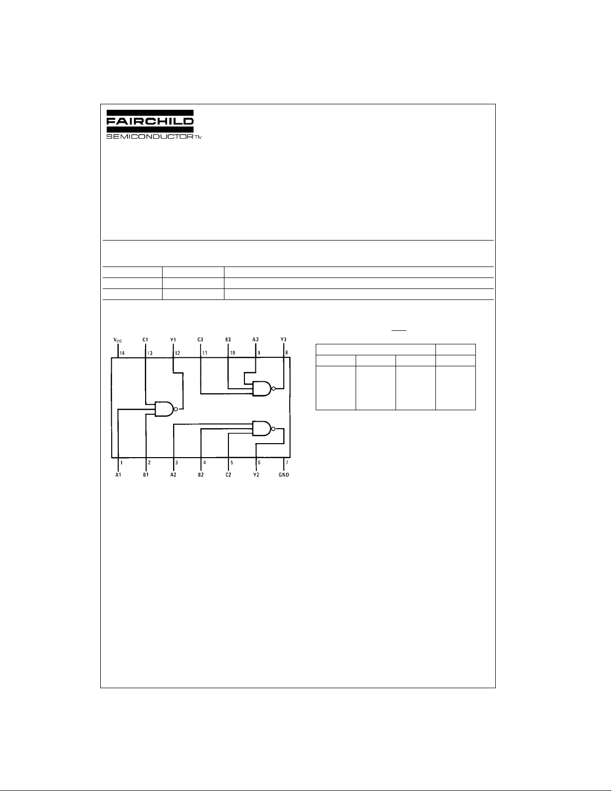
Connection Diagram Function Table
Y = ABC
Inputs Output
ABCY
XXLH
XLXH
LXXH
HHHL
H = HIGH Logic Level
L = LOW Logic Level
X = Either LOW or HIGH Logic Level
DM74LS10 Tri ple 3-Input NAND Gate
© 2000 Fairchild Semiconductor Corporation DS006349 www.fairchildsemi.com
Page 2
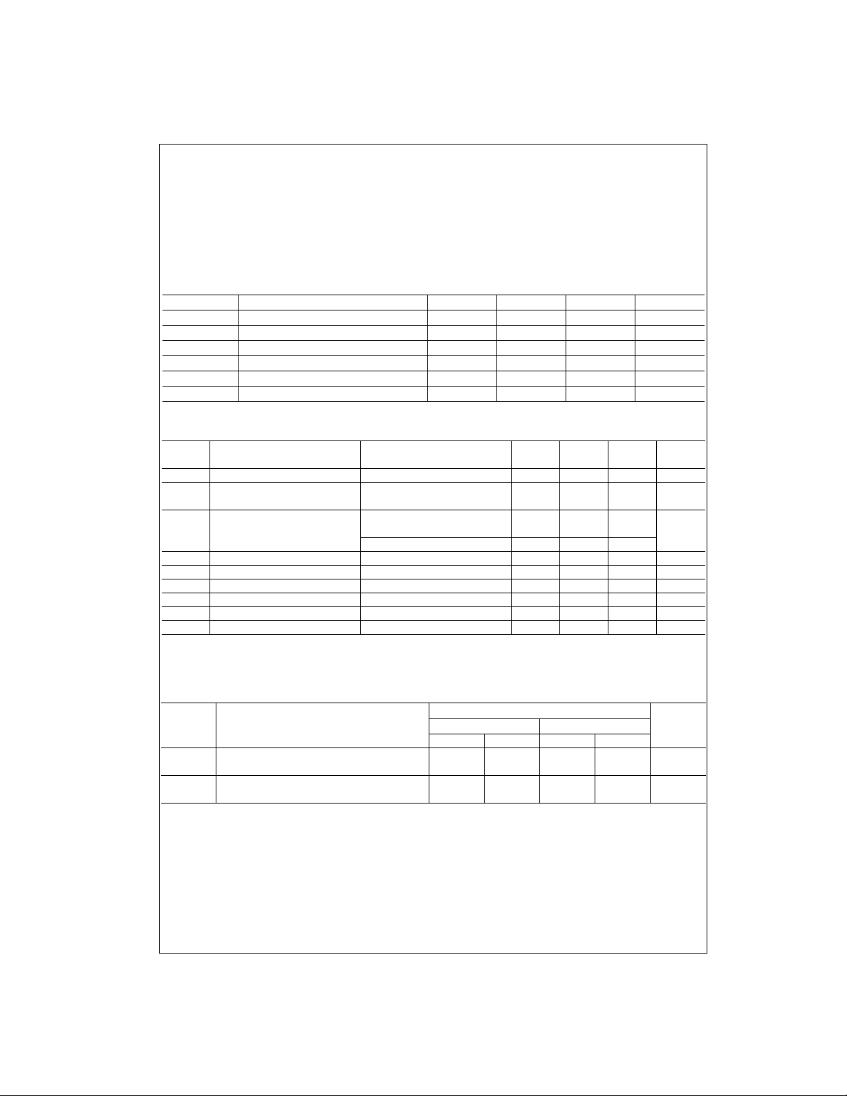
Absolute Maximum Ratings(Note 1)
Supply Voltage 7V
Input Voltage 7V
Operating Free Air Temperature Range 0°C to +70°C
DM74LS10
Storage Temperature Range −65°C to +150°C
Note 1: The “Absolute Maximum Ratin gs” are those v alues beyon d which
the safety of the dev ice cannot be guaranteed. T he device sh ould not be
operated at these limits. The parametric values defined in the Electrical
Characteristics tables are not guaranteed at the absolute maximum ratings.
The “Recommend ed O peratin g Cond itions” t able w ill defin e the c ondit ions
for actual device operation.
Recommended Operating Conditions
Symbol Parameter Min Nom Max Units
V
CC
V
IH
V
IL
I
OH
I
OL
T
A
Supply Voltage 4.75 5 5.25 V
HIGH Level Input Voltage 2 V
LOW Level Input Voltage 0.8 V
HIGH Level Output Current −0.4 mA
LOW Level Output Current 8 mA
Free Air Operating Temperature 0 70 °C
Electrical Characteristics
over recommended operating free air temperature range (unless otherwise noted)
Symbol Parameter Conditions Min
V
I
V
OH
V
OL
I
I
I
IH
I
IL
I
OS
I
CCH
I
CCL
Note 2: All typicals are at VCC = 5V, TA = 25°C.
Note 3: Not more than one output should be shorted at a time, and the duration should not exceed one second.
Input Clamp Voltage VCC = Min, II = −18 mA −1.5 V
HIGH Level VCC = Min, IOH = Max,
Output Voltage VIL = Max
LOW Level VCC = Min, IOL = Max,
Output Voltage VIH = Min V
IOL = 4 mA, VCC = Min 0.25 0.4
Input Current @ Max Input Voltage VCC = Max, VI = 7V 0.1 mA
HIGH Level Input Current VCC = Max, VI = 2.7V 20 µA
LOW Level Input Current VCC = Max, VI = 0.4V −0.36 mA
Short Circuit Output Current VCC = Max (Note 3) −20 −100 mA
Supply Current with Outputs High VCC = Max 0.6 1.2 mA
Supply Current with Outputs Low VCC = Max 1.8 3.3 mA
2.7 3.4 V
Typ
(Note 2)
0.35 0.5
Max Units
Switching Characteristics
at VCC = 5V and TA = 25°C
Symbol Parameter
t
PLH
t
PHL
www.fairchildsemi.com 2
Propagation Delay Time
LOW-to-HIGH Level Output
Propagation Delay Time
HIGH-to-LOW Level Output
RL = 2 kΩ
CL = 15 pF CL = 50 pF
Min Max Min Max
310415ns
310415ns
Units
Page 3
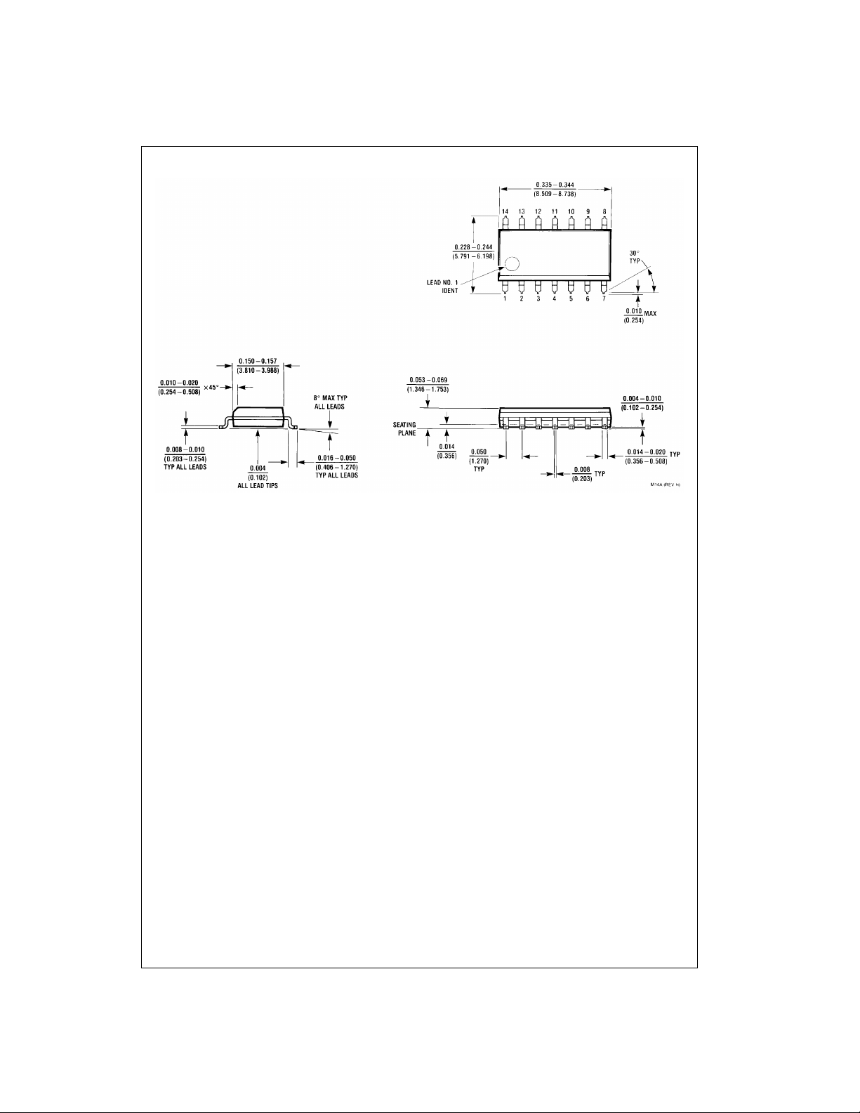
Physical Dimensions inches (millimeters) unless otherwise noted
DM74LS10
14-Lead Small Outline Integrated Circuit (SOIC), JEDEC MS-120, 0.150 Narrow
Package Number M14A
3 www.fairchildsemi.com
Page 4
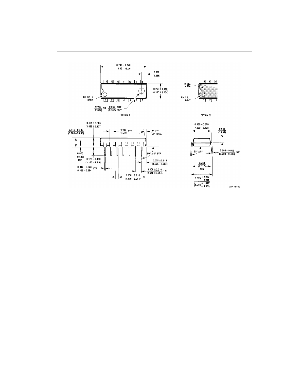
Physical Dimensions inches (millimeters) unless otherwise noted (Continued)
DM74LS10 Triple 3-Input NAND Gate
14-Lead Plastic Dual-In-Line Package (PDIP), JEDEC MS-001, 0.300 Wide
Fairchild does not assume any responsibility for us e of any circuitry described, no circuit patent licenses are implied and
Fairchild reserves the right at any time without notice to change said circuitry and specifications.
LIFE SUPPORT POLICY
FAIRCHILD’S PRODUCTS ARE NOT AUTHORIZED FOR USE AS CRITICAL COMPONENTS IN LIFE SUPPORT
DEVICES OR SYSTEMS WITHOUT THE EXPRESS WRITTEN APPROVAL OF THE PRESIDENT OF FAIRCHILD
SEMICONDUCTOR CORPORATION. As used herein:
1. Life support devices or systems are devices or syste ms
which, (a) are intended for surgical implant into the
body, or (b) support or sustain life, and (c) whose failure
to perform when properly used in accordance with
instructions for use provided in the labeling, can be reasonably expected to result in a significan t injury to the
user.
Package Number N14A
2. A critical component in any compon ent of a lif e supp ort
device or system whose failu re to perform can be reasonably expected to ca use the fa i lure of the li fe su pp ort
device or system, or to affect its safety or effectiveness.
www.fairchildsemi.com
www.fairchildsemi.com 4
 Loading...