

Page 1
© 2000 Fairchild Semiconductor Corporation DS009174 www.fairchildsemi.com
October 1986
Revised March 2000
DM74ALS652 Octal 3-STATE Bus Transceiver and Register
DM74ALS652
Octal 3-STATE Bus Transceiver and Register
General Description
This device incorpora tes an octal t ransceiver a nd an octal
D-type register configured to enable transmission of data
from bus to bus or internal register to bus.
This bus transceiver features totem-p ole 3-STATE outputs
designed specifically fo r driving highly-capacitive or relatively low-impedance loa ds. Th e hi gh -im ped ance state and
increased high level logic drive provide this device with the
capability of being connected directly to and driving the bus
lines in a bus organized system with out need for interfa ce
or pull-up components. They are par ticularly attractive for
implementing buffer registers, I/O ports, bidirectional bus
drivers, and working registers.
The registers in the DM74 ALS652 are edge-triggered Dtype flip-flops. On the positive tra nsition of the clock ( CAB
or CBA), the input data is stored into the appropr i ate reg ister. The CAB input controls the trans fer of data into the A
register and the CBA input controls the B register.
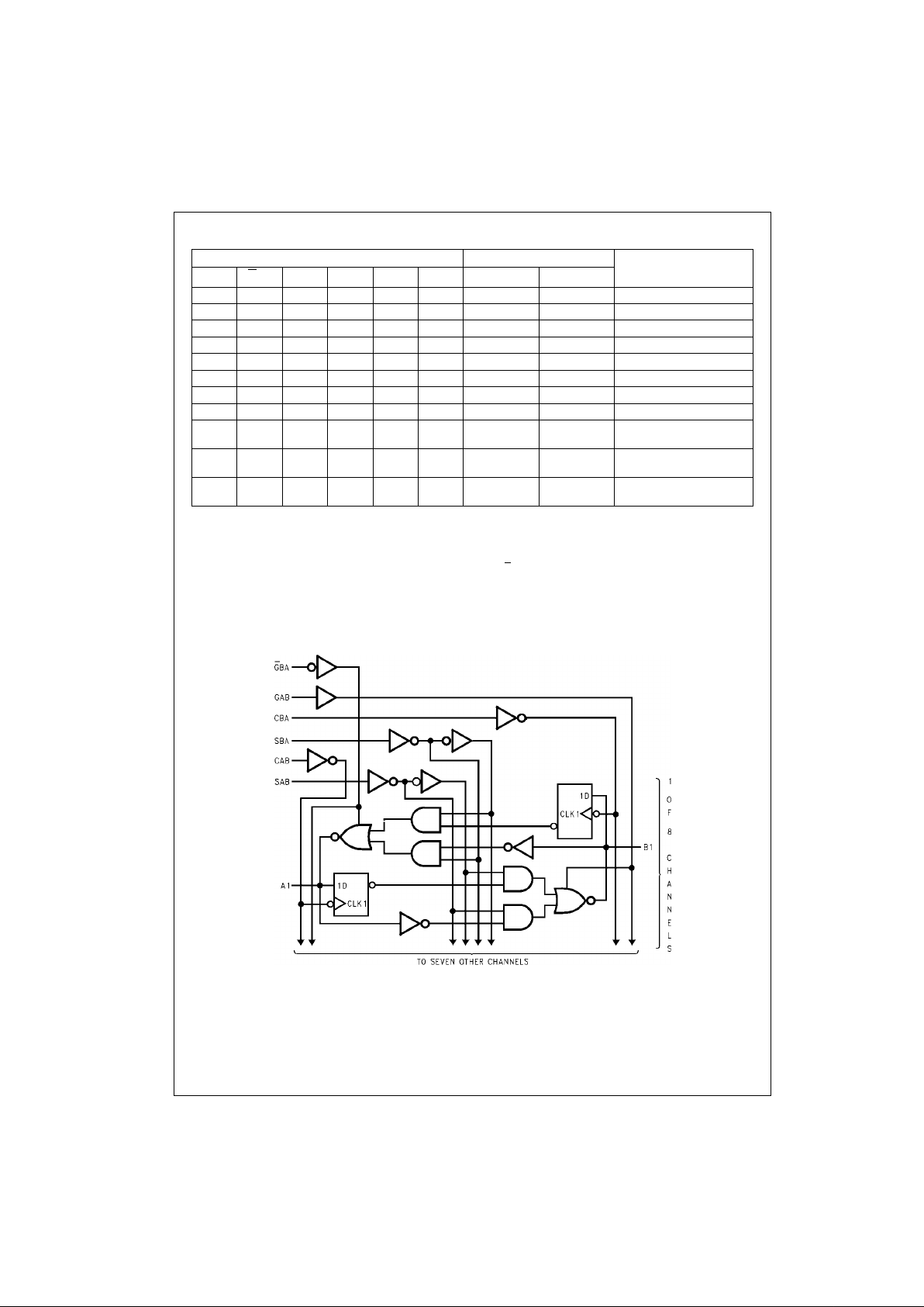
The SAB and SBA control pins are provided to select
whether real-time data or stored data is transferred. A LOW
input level selects real-time data and a HIGH level selects
stored data. The select controls have a “make before
break” configuration to eliminate a glitch which wo uld normally occur in a typical multiplexer during the transition
between stored and real-time data.
The enable (GAB and G
BA) control pins provide four
modes of operation: r eal-time data transfe r from bus A to
B, real-time data t ransfer from bus B to A, real-ti me bus A
and/or B data transfer to internal storage, or internal stored
data transfer to bus A and/or B.
Features
■ Switching specifications at 50 pF
■ Switching specifications guaranteed over full tempera-
ture and V
CC
range
■ Advanced oxide-isolated, ion-implanted Schottky TTL
process
■ 3-STATE buffer-type outputs drive bus lines directly
■ Independent registers and enables for A and B buses
■ Multiplexed real-time and stored data
Ordering Code:
Devices also availab le in Tape and Reel. Specify by appending th e s uffix let t er “X” to the ordering code.
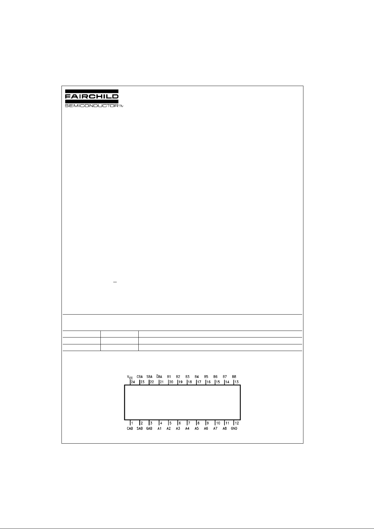
Connection Diagram
Order Number Package Number Package Description
DM74ALS652WM M24B 24-Lead Small Outline Integrated Circuit (SOIC), JEDEC MS-013, 0.300 Wide
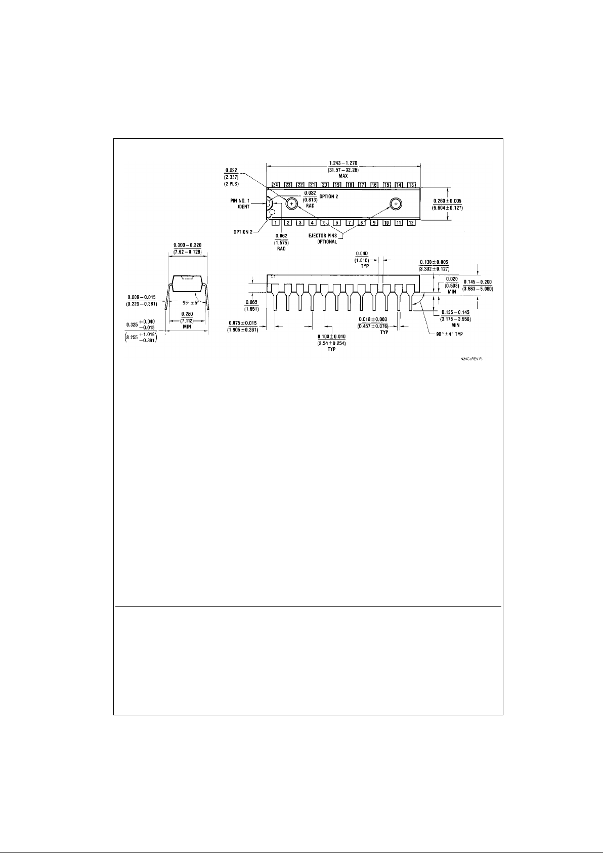
DM74ALS652NT N24C 24-Lead Plastic Dual-In-Line Package (PDIP), JEDEC MS-100, 0.300 Wide
Page 2
www.fairchildsemi.com 2
DM74ALS652
Function Table
H = HIGH Logic Level
L = LOW Logic Level
X = Don’t Care (Either LOW or HIGH Logic Levels, inc luding transitions)
H/L = Either LOW or HIGH Logic Level excluding transitions
↑ = Positive-going edge of pulse
Note 1: The data output functions may be enabled or disabled by various signals at the G
and DIR inputs. Data input functions are always enabled,
i.e., data at the bus pins w ill be stored on every LOW-to-HIGH transition on the clock inputs.
Note 2: Select control = L; clocks can oc c ur s im ultaneously
Select control = H; clocks must be staggered in order to load both registers.
Logic Diagram
Inputs Data I/O (Note 1)
Operation or Function
GAB G
BA CAB CBA SAB SBA A1 thru A8 B1 thru B8
XH↑ H/L X X Input Not Specified Store A, Hold B
LXH/L↑ X X Not Specified Input Store B, Hold A
LH↑↑X X Input Input Store A and B Data
L H H/L H/L X X Input Input Isolation, Hold Storage
L L X X X L Output Input Real-Time B Data to A Bus
L L X H/L X H Output Input Stored B Data to A Bus
H H X X L X Input Output Real-Time A Data to B Bus
HH↑↑X X Input Output Stored A Data to B Bus
HH↑↑X
(Note 2)
X Input Output Store A in both Registers
LL↑↑XX
(Note 2)
Output Input Store B in both Registers
H L H or L H or L H H Output Output Stored A Data to B Bus and
Stored B Data to A Bus
Page 3
3 www.fairchildsemi.com
DM74ALS652
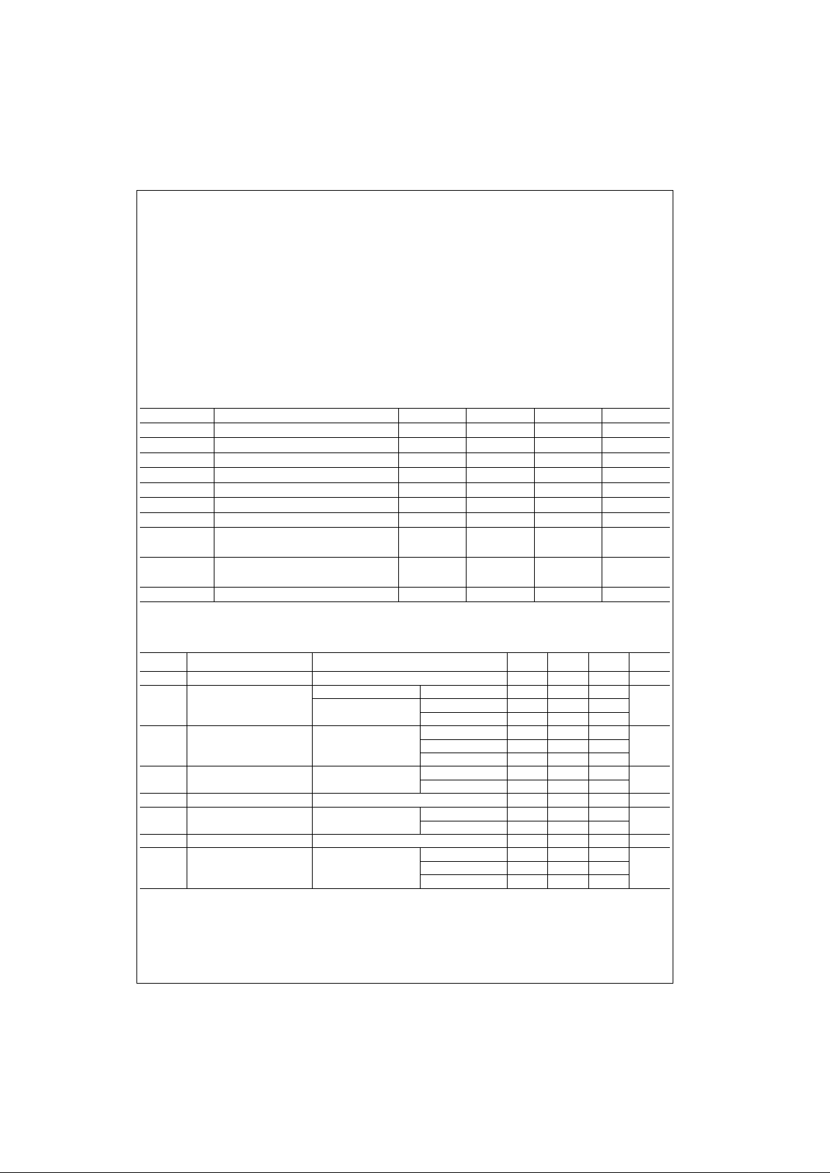
Absolute Maximum Ratings(Note 3)
Note 3: The “Absolute Maximum Ratings ” are those val ues beyond w hich
the safety of the device cannot be guaranteed. The device should not be
operated at these limits. The parametric values defined in the Electrical
Characteristics tables are not guaranteed at the absolute maximum ratings.
The “Recommend ed O peratin g Cond itions” t able w ill defin e the condition s
for actual device operation.
Recommended Operating Conditions
Note 4: ↑ = with reference to the LOW-to-HIGH transition of the respective clock.
Electrical Characteristics
over recommended free air temperature range
Note 5: For I/O ports the 3-STATE output currents (I
OZH
and I
OZL
) are included in the IIH and IIL parameters.
Supply Voltage 7V
Input Voltage
Control Inputs 7V
I/O Ports 5.5V
Operating Free-Air Temperature Range 0°C to +70°C
Storage Temperature Range −65°C to +150°C
Typical θ
JA
N Package 44.5°C/W
M Package 80.5°C/W
Symbol Parameter Min Nom Max Units
V
CC
Supply Voltage 4.5 5 5.5 V
V
IH
HIGH Level Input Voltage 2 V
V
IL
LOW Level Input Volta ge 0.8 V
I
OH
HIGH Level Output Current −15 mA
I
OL
LOW Level Output Current 24 mA
f
CLK
Clock Frequency 0 40 MHz
t
W
Pulse Duration, Clocks Low or High 12.5 ns
t
SU
Data Setup Time, A before CAB or 10↑ ns
B before CBA (Note 4)
t
H
Data Hold Time, A after CAB or 0↑ ns
B after CBA (Note 4)
T
A
Free Air Operating Temperature 0 70 °C
Symbol Parameter Test Conditions Min Typ Max Units
V
IK
Input Clamp Voltage VCC = Min, II = −18 mA −1.2 V
V
OH
HIGH Level VCC = 4.5V to 5.5V IOH = −0.4 mA VCC − 2
Output Voltage VCC = Min IOH = −3 mA 2.4 3.2 V
IOH = Max 2
V
OL
LOW Level VCC = Min IOL = 12 mA 0.25 0.4
Output Voltage IOL = 24 mA 0.35 0.5 V
IOL = 48 mA 0.35 0.5
I
I
Input Current at Maximum VCC = Max I/O Ports, VI = 5.5V 100
µA
Input Voltage Control Inputs, VI = 7V 100
I
IH
HIGH Level Input Current VCC = Max, VI = 2.7V, (Note 5) 20 µA
I
IL
LOW Level VCC = Max, Control Inputs −200
µA
Input Current VI = 0.4V (Note 5) I/O Ports −200
I
O
Output Drive Current VCC = Max, VO = 2.25V −30 −112 mA
I
CC
Supply Current VCC = Max Outputs HIGH 47 76
Outputs LOW 55 88 mA
Outputs Disabled 55 88
Page 4

www.fairchildsemi.com 4
DM74ALS652
Switching Characteristics
over recommended operating free air temperature range (Note 6)
Note 6: These para m et ers are measured wit h th e internal output state of t he s t orage register oppos ite to th at of th e bus input.
Symbol Parameter Conditions
From (Input)
Min
Max
Units
To (Output)
t
PLH
Propagation Delay Time VCC = 4.5V to 5.5V, CBA or CAB
10 30 ns
LOW-to-HIGH Level Output CL = 50 pF, to A or B
t
PHL
Propagation Delay Time R1 = R2 = 500Ω,CBA or CAB
517ns
HIGH-to-LOW Level Output TA = Min to Max to A or B
t
PLH
Propagation Delay Time A or B to
518ns
LOW-to-HIGH Level Output B or A
t
PHL
Propagation Delay Time A or B to 3 12 ns
HIGH-to-LOW Level Output B or A
t
PLH
Propagation Delay Time
LOW-to-HIGH Level Output SBA or SAB 1 2 35 ns
(with A or B LOW) (Note 6) to A or B
t
PHL
Propagation Delay Time
HIGH-to-LOW Level Output SBA or SAB 6 20 ns
(with A or B LOW) (Note 6) to A or B
t
PLH
Propagation Delay Time
LOW-to-HIGH Level Output SBA or SAB 6 25 ns
(with A or B HIGH) (Note 6) to A or B
t
PHL
Propagation Delay Time
HIGH-to-LOW Level Output SBA or SAB 5 20 ns
(with A or B HIGH) (Note 6) to A or B
t
PZH
Output Enable Time GBA to
317ns
to HIGH Level Output A
t
PZL
Output Enable Time GBA to
518ns
to LOW Level Output A
t
PHZ
Output Disable Time GBA to
110ns
from HIGH Level Output A
t
PLZ
Output Disable Time GBA to
216ns
from LOW Level Output A
t
PZH
Output Enable Time GAB to
622ns
to HIGH Level Output B
t
PZL
Output Enable Time GAB to
618ns
to LOW Level Output B
t
PHZ
Output Disable Time GAB to
110ns
from HIGH Level Output B
t
PLZ
Output Disable Time GAB to
216ns
from LOW Level Output B
Page 5
5 www.fairchildsemi.com
DM74ALS652
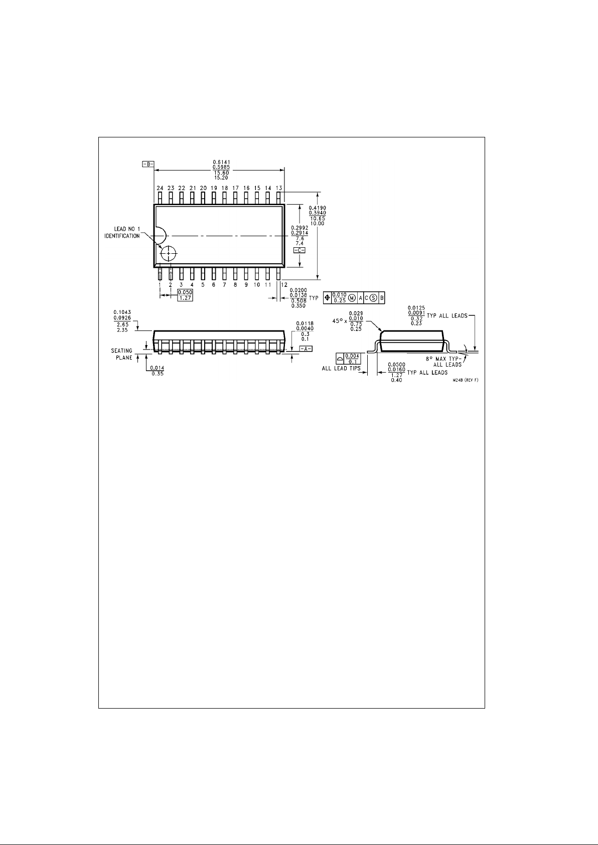
Physical Dimensions inches (millimeters) unless otherwise noted
24-Lead Small Outline Integrated Circuit (SOIC), JEDEC MS-013, 0.300 Wide
Package Number M24B
Page 6
www.fairchildsemi.com 6
DM74ALS652 Octal 3-STA TE Bus Transceiver and Register
Physical Dimensions inches (millimeters) unless otherwise noted (Continued)
24-Lead Plastic Dual-In-Line Package (PDIP), JEDEC MS-100, 0.300 Wide
Package Number N24C
Fairchild does not assume any responsibility for use of any circuitry described, no circuit pate nt licenses are implied and
Fairchild reserves the right at any time without notice to change said circuitry and specifications.
LIFE SUPPORT POLICY
FAIRCHILD’S PRODUCTS ARE NOT AUTHORIZED FOR USE AS CRITICAL COMPONENTS IN LIFE SUPPORT
DEVICES OR SYSTEMS WITHOUT THE EXPRESS WRITTEN APPROVAL OF THE PRESIDENT OF FAIRCHILD
SEMICONDUCTOR CORPORATION. As used herein:
1. Life support devices or systems are devices or syste ms
which, (a) are intended for surgical implant into the
body, or (b) support or sustain life, and (c) whose failure
to perform when properly used in accordance with
instructions for use provided in the labeling, can be reasonably expected to result in a significant inju ry to the
user.
2. A critical component i n any compon ent of a lif e support
device or system whose failu re to perform can be reasonably expected to ca use the fa i lure of the life su pp ort
device or system, or to affect its safety or effectiveness.
www.fairchildsemi.com
 Loading...