

Page 1
© 2000 Fairchild Semiconductor Corporation DS006207 www.fairchildsemi.com
April 1984
Revised April 2000
DM74ALS169B Synchronous Four-Bit Up/Down Counters
DM74ALS169B
Synchronous Four-Bit Up/Down Counters
General Description
These synchronous p resettable counters feature an internal carry look ahe ad for c ascading in high speed count ing
applications. The DM74ALS169B is a four-bit binary up/
down counter. The carry output is decoded to prevent
spikes during normal mode of counting operation. Synchronous operation is provide d so that outputs change coincident with each other when so instructed by count enable
inputs and internal gating. This mode of operation eliminates the output counti ng spikes wh ich are norm ally associated with asynchronous (ripple clock) counters. A
buffered clock input triggers th e four flip-flops o n the rising
(positive going) edge of clock input waveform.
These counters are fully programmable; that is, the outputs
may each be preset either HIGH or LOW. The load input
circuitry allows loading with carry-enable output of cascaded counters. As loading is synchr onous, setting up a
low level at the load input disables the counte r a nd causes
the outputs to agree with the data inputs after the next
clock pulse.
The carry look-ahead circuitr y permits cascading counters
for n-bit synchronous applications without additional gating.
Both count enable inputs (P
and T) must be LOW to count.
The direction of the co unt is determ ined b y the l evel of t he
up/down input. When the input is HIGH, the counter counts
UP; when LOW, it counts DOWN . Inpu t T is fed fo rward to
enable the carry outputs. The carry output thus enabled will
produce a low level o utput pulse with a dura tion approximately equal to the high p ortion of the Q
A
output when
counting UP, and approximately equal to the low portion of
the Q
A
when counting DOWN. This low level overflow carry
pulse can be used to enable successively cascaded
stages. Transitions at the enable P
or T inputs are allowed
regardless of the level of the clock input.
The control function s for thes e counters a re fully synchr o-
nous. Changes at control inpu ts (enab le P
, enable T, load,
up/down) which modify the opera ting mode have no effect
until clocking occurs. The func tion of the counte r (whether
enabled, disabled, loading or counting) will be dictated
solely by the conditions meeting the stable setup and hold
times.
Features
■ Switching specifications at 50 pF
■ Switching specifications guaranteed over full tempera-
ture and V
CC
range
■ Advanced oxide-isolated, ion-implanted Schottky TTL
process
■ Functionally and pin-for-pin compatible with Schottky
and low power Schottky TTL counterpart
■ Improved AC performa nce over S cho ttky a nd low p ower
Schottky counterparts
■ Synchronously programmable
■ Internal look ahead for fast counting
■ Carry out put for n-bit cascading
■ Synchronous counting
■ ESD inputs
Ordering Code:
Devices also availab le in Tape and Reel. Specify by appending th e s uffix let t er “X” to the ordering code.
Order Number Package Number Package Description
DM74ALS169BM M16A 16-Lead Small Outline Integrated Circuit (SOIC), JEDEC MS-012, 0.150 Narrow
DM74ALS169BN N16E 16-Lead Plastic Dual-In-Line Package (PDIP), JEDEC MS-001, 0.300 Wide
Page 2
www.fairchildsemi.com 2
DM74ALS169B
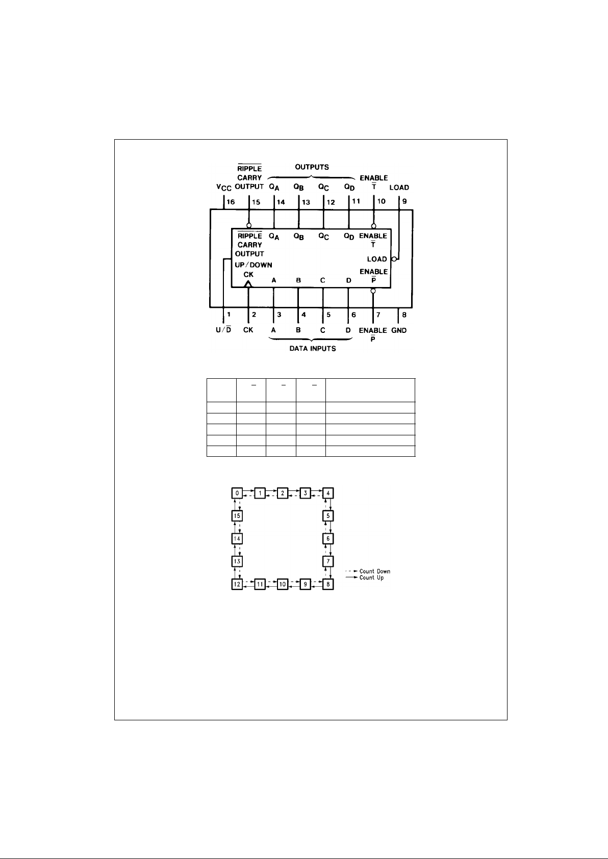
Connection Diagram
Mode Select Table
State Diagram
LOAD EP ET U/D
Action on Rising
Clock Edge
LXXXLoad (P
n
→ Qn)
H L L H Count Up (Increment)
H L L L Count Down (Decrement)
H H X X No Change (Hold)
H X H X No Change (Hold)
Page 3
3 www.fairchildsemi.com
DM74ALS169B
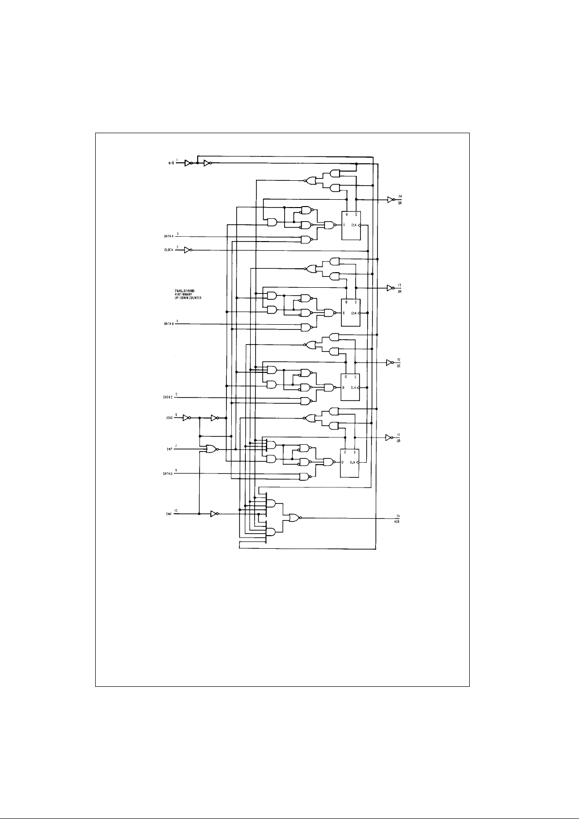
Logic Diagram
Page 4

www.fairchildsemi.com 4
DM74ALS169B
Absolute Maximum Ratings(Note 1)
Note 1: The “Absolute Maximum Ratings” are those values beyon d which
the safety of the dev ice cannot be guaranteed. T he device sh ould not be
operated at these limit s. The parametric values defin ed in the Electrical
Characteristics tables are not guaranteed at the absolute maximum ratings.
The “Recomme nded O peratin g Cond itions ” table will defin e the condition s
for actual device operation.
Recommended Operating Conditions
Note 2: The symbol (↑) indicates tha t t he rising edge of t he clock is used as reference.
Supply Voltage 7V
Input Voltage 7V
Operating Free Air Temperature Range 0°C to +70°C
Storage Temperature Range −65°C to +150°C
Typical θ
JA
N Package 78.1°C/W
M Package 106.8°C/W
Symbol Parameter Min Nom Max Units
V
CC
Supply Voltage 4.5 5 5.5 V
V
IH
HIGH Level Input Voltage 2 V
V
IL
LOW Level Input Voltage 0.8 V
I
OH
HIGH Level Output Current −0.4 mA
I
OL
LOW Level Output Current 8 mA
f
CLK
Clock Frequency 0 40 MHz
t
SU
Setup Time (Note 2) Data;
15↑ 6ns
A, B, C, D
En P
, En T 15↑ 8ns
Load
15↑ 8ns
U/D
15↑ 10 ns
t
H
Hold Time (Note 2) Data;
0↑−3ns
A, B, C, D
En P
, En T 0↑−3ns
Load
0↑−4ns
U/D
0↑−4ns
t
W
Width of Clock Pulse 13 ns
Page 5

5 www.fairchildsemi.com
DM74ALS169B
Electrical Characteristics
over recommended operating free air temperature range. All typical values are measured at V
CC
= 5V, T
A
= 25°C
Switching Characteristics
over recommended operating free air temperature range
Note 3: Propagation delay time from up/down to ripple carry must be m easured with the counte r at eith er a minimum or a maximum co unt. As the logic level
of the up/down input is changed, the ripple carry output will follow. If the count is minimum (0), the ripple carry output transition will be in phase. If the count is
maximum, the ripple ca rry output will be out of phase .
Symbol Parameter Conditions Min Typ Max Units
V
IK
Input Clamp Voltage VCC = 4.5V, II = −18 mA −1.5 V
V
OH
HIGH Level IOH = −0.4 mA
V
CC
− 2V
Output Voltage VCC = 4.5V to 5.5V
V
OL
LOW Level
VCC = 4.5V IOL = 8 mA 0.35 0.5 V
Output Voltage
I
I
Input Current @ Max
V
CC
= 5.5V, VIH = 7V 0.1 mA
Input Voltage
I
IH
HIGH Level Input Current VCC = 5.5V, VIH = 2.7V 20 µA
I
IL
LOW Level Input Current VCC = 5.5V, VIL = 0.4V −0.2 mA
I
O
Output Drive Current VCC = 5.5V, VO = 2.25V −30 −112 mA
I
CC
Supply Current VCC = 5.5V 15 25 mA
Symbol Parameter Conditions From To Min Max Units
f
MAX
Maximum Clock Frequency 40 MHz
t
PLH
Propagation Delay Time VCC = 4.5V to 5.5V
Clock Ripple Carry 3 20 ns
LOW-to-HIGH Level Output R
L
= 500Ω
t
PHL
Propagation Delay Time CL = 50 pF
Clock Ripple
Carry 6 20 ns
HIGH-to-LOW Level Output
t
PLH
Propagation Delay Time
Clock Any Q 2 15 ns
LOW-to-HIGH Level Output
t
PHL
Propagation Delay Time
Clock Any Q 5 20 ns
HIGH-to-LOW Level Output
t
PLH
Propagation Delay Time
En T Ripple Carry 2 13 ns
LOW-to-HIGH Level Output
t
PHL
Propagation Delay Time
En T Ripple
Carry 3 16 ns
HIGH-to-LOW Level Output
t
PLH
Propagation Delay Time
U/D
(Note 3) Ripple Carry 5 19 ns
LOW-to-HIGH Level Output
t
PHL
Propagation Delay Time
U/D (Note 3) Ripple Carry 5 19 ns
HIGH-to-LOW Level Output
Page 6

www.fairchildsemi.com 6
DM74ALS169B
Physical Dimensions inches (millimeters) unless otherwise noted
16-Lead Small Outline Integrated Circuit (SOIC), JEDEC MS-012, 0.150 Narrow
Package Number M16A
Page 7

7 www.fairchildsemi.com
DM74ALS169B Synchronous Four-Bit Up/Down Counters
Physical Dimensions inches (millimeters) unless otherwise noted (Continued)
16-Lead Plastic Dual-In-Line Package (PDIP), JEDEC MS-001, 0.300 Wide
Package Number N16E
Fairchild does not assume any responsibility for use of any circuitry described , no circuit patent licenses are implied and
Fairchild reserves the right at any time without notice to change said circuitry and specifications.
LIFE SUPPORT POLICY
FAIRCHILD’S PRODUCTS ARE NOT AUTHORIZED FOR USE AS CRITICAL COMPONENTS IN LIFE SUPPORT
DEVICES OR SYSTEMS WITHOUT THE EXPRESS WRITTEN APPROVAL OF THE PRESIDENT OF FAIRCHILD
SEMICONDUCTOR CORPORATION. As used herein:
1. Life support devices or systems are dev ic es or syste ms
which, (a) are intended for surgical implant into the
body, or (b) support or sustain life, and (c) whose failure
to perform when properly used in accordance with
instructions for use provide d in the labe l ing, can be re asonably expected to result in a significant injury to the
user.
2. A critical compo nent in any com ponen t of a life s upp ort
device or system whose failure to perform can be reasonably expected to cause the failure of the l ife support
device or system, or to affect its safety or effectiveness.
www.fairchildsemi.com
 Loading...