

Datasheet DM74ALS153SJ, DM74ALS153N, DM74ALS153MX, DM74ALS153M Datasheet (Fairchild Semiconductor)
Page 1
© 2000 Fairchild Semiconductor Corporation DS006204 www.fairchildsemi.com
April 1984
Revised February 2000
DM74ALS153 Dual 1-of-4 Line Data Selector/Multiplexer
DM74ALS153
Dual 1-of-4 Line Data Selector/Multiplexer
General Description
This Data Selector/Multi plexer contain s full on-chip decoding to select one-of-four data sources as a result of a
unique two-bit binary code at the Select inputs. Each of the
two Data Selector/Multipl e xer c irc uits have the i r own sep arate Data and Strobe inputs and a non-inverting output
buffer. The Select inputs A and B are common to both sections. The Strobe inputs, whe n at the HIGH level, disable
their associated data inputs and force the corresponding
output to the LOW st ate. The Select inp ut buffers inco rporate internal overlap featu res to ensure that select input
changes do not cause invalid output transients.
Features
■ Advanced oxide-isolated, ion-implanted Schottky TTL
process
■ Switching performan ce is gu aranteed over full tempe rature and V
CC
supply range
■ Pin and functional compatible with LS family counterpart
■ Improved output transient handling capability
Ordering Code:
Devices also availab le in Tape and Reel. Specify by appending th e s uffix let t er “X” to the ordering code.
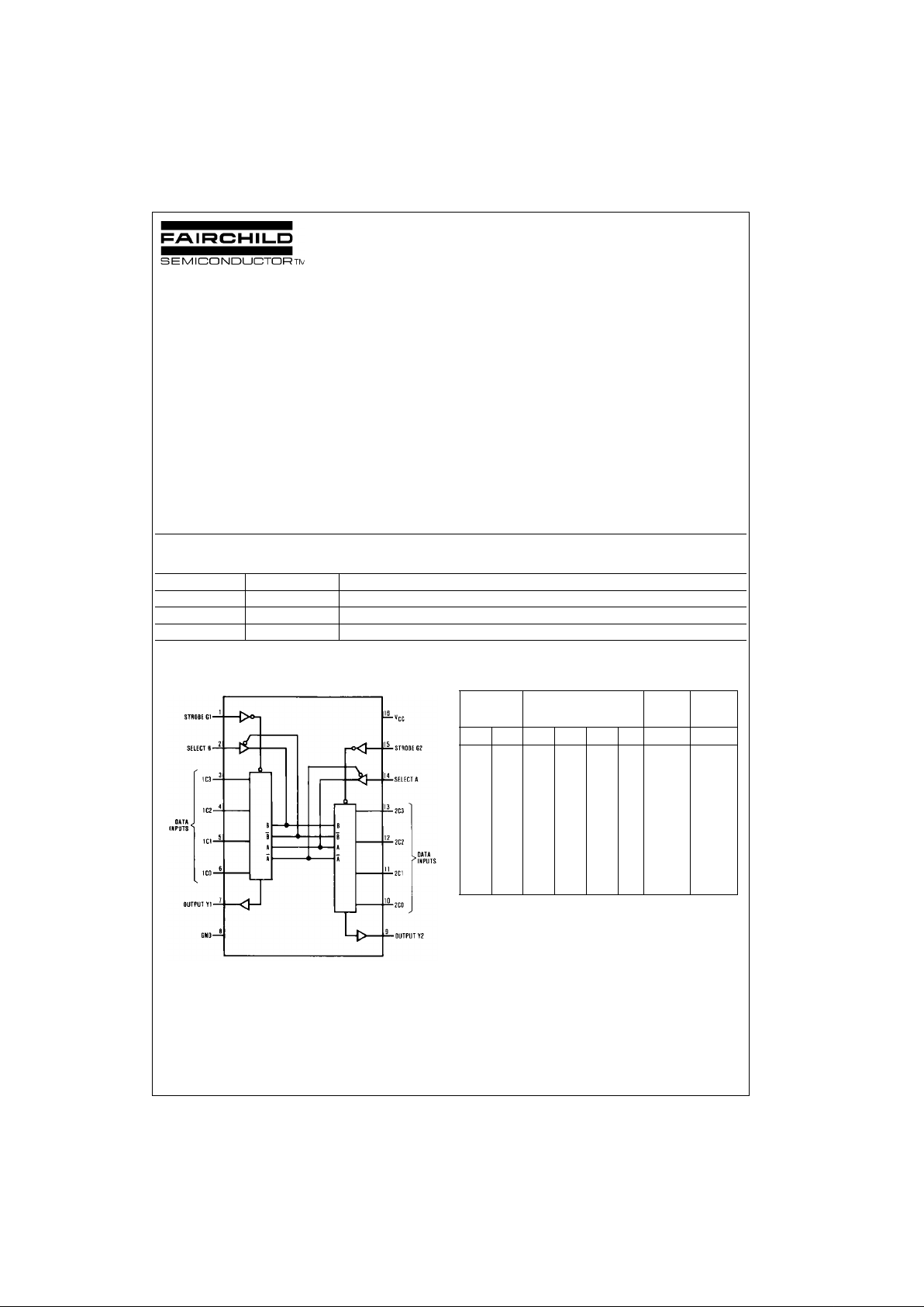
Connection Diagram Function Table
Select inputs A and B are common to both sections.
H = HIGH Level
L = LOW Level
X = Don't Care
Order Number Package Number Package Description
DM74ALS153M M16A 16-Lead Small Outline Integrated Circuit (SOIC), JEDEC MS-012, 0.150 Narrow
DM74ALS153SJ M16D 16-Lead Small Outline Package (SOP), EIAJ TYPE II, 5.3mm Wide
DM74ALS153N N16E 16-Lead Plastic Dual-In-Line Package (PDIP), JEDEC MS-001, 0.300 Wide
Select
Data Inputs Strobe Output
Inputs
B A C0 C1 C2 C3 G Y
XXXXXX H L
LLLXXX L L
LLHXXX L H
LHXLXX L L
LHXHXX L H
HLXXLX L L
HLXXHX L H
HHXXXL L L
HHXXXH L H
Page 2
www.fairchildsemi.com 2
DM74ALS153
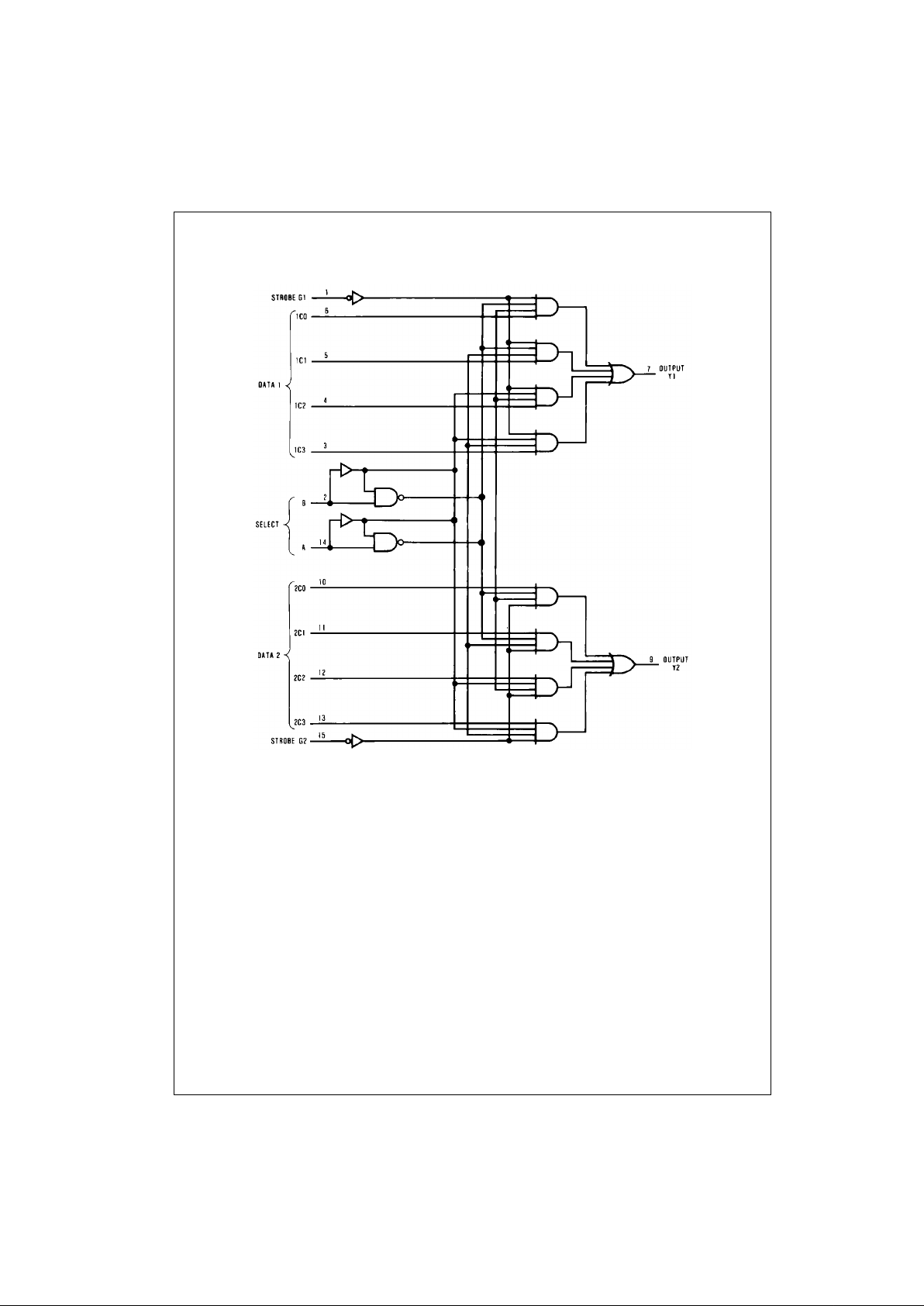
Logic Diagram
Page 3

3 www.fairchildsemi.com
DM74ALS153
Absolute Maximum Ratings(Note 1)
Note 1: The “Absolute M aximu m R atin gs” are t hose valu es b eyo nd w hich
the safety of the device cannot be guaranteed. The device should not be
operated at these limits. The parametric values defined in the Electrical
Characteristics tables are not guaranteed at the absolute maximum ratings.
The “Recommend ed O peratin g Cond itions” t able w ill defin e the condition s
for actual device operation.
Recommended Operating Conditions
Electrical Characteristics
over recommended operating free air temperature range. All typical values are measured at VCC = 5V, TA = 25°C.
Switching Characteristics
over recommended operating free air temperature range.
Supply Voltage 7V
Input Voltage 7V
Operating Free Air Temperature Range 0°C to +70°C
Storage Temperature Range −65°C to +150°C
Typical θ
JA
N Package 78.0°C/W
M Package 107.0°C/W
Symbol Parameter Min Nom Max Units
V
CC
Supply Voltage 4.5 5 5.5 V
V
IH
HIGH Level Input Voltage 2 V
V
IL
LOW Level Input Voltage 0.8 V
I
OH
HIGH Level Output Current −2.6 mA
I
OL
LOW Level Output Current 24 mA
T
A
Free Air Operating Temperature 0 70 °C
Symbol Parameter Conditions Min Typ Max Units
V
IK
Input Clamp Voltage VCC = 4.5V, IIN = −18 mA −1.5 V
V
OH
HIGH Level VCC = 4.5V, IOH = Max 2.4 3.2 V
Output Voltage IOH = −400 µA, VCC = 4.5V to 5.5V VCC − 2V
V
OL
LOW Level
VCC = 4.5V IOL = 24 mA 0.35 0.5 V
Output Voltage
I
I
Input Current at
VCC = 5.5V, VIN = 7V 0.1 mA
Max Input Voltage
I
IH
High Level Input Current VCC = 5.5V, VIN = 2.7V 20 µA
I
IL
Low Level Input Current VCC = 5.5V, VIN = 0.4V −0.1 mA
I
O
Output Drive Current VCC = 5.5V, V
OUT
= 2.25V −30 −112 mA
I
CC
Supply Current VCC = 5.5V
7.5 14 mA
All Inputs = 4.5V
Symbol Parameter Conditions From To Min Max Units
t
PLH
Propagation Delay Time VCC = 4.5V to 5.5V
Select Y 5 21 ns
LOW-to-HIGH Level Output CL = 50 pF
t
PHL
Propagation Delay Time RL = 500Ω
Select Y 5 21 ns
HIGH-to-LOW Level Output
t
PLH
Propagation Delay Time
Data Y 3 10 ns
LOW-to-HIGH Level Output
t
PHL
Propagation Delay Time
Data Y 4 15 ns
HIGH-to-LOW Level Output
t
PLH
Propagation Delay Time
Strobe Y 5 18 ns
LOW-to-HIGH Level Output
t
PHL
Propagation Delay Time
Strobe Y 5 18 ns
HIGH-to-LOW Level Output
Page 4

www.fairchildsemi.com 4
DM74ALS153
Physical Dimensions inches (millimeters) unless otherwise noted
16-Lead Small Outline Integrated Circuit (SOIC), JEDEC MS-012, 0.150 Narrow
Package Number M16A
Page 5

5 www.fairchildsemi.com
DM74ALS153
Physical Dimensions inches (millimeters) unless otherwise noted (Continued)
16-Lead Small Outline Package (SOP), EIAJ TYPE II, 5.3mm Wide
Package Number M16D
Page 6

www.fairchildsemi.com 6
DM74ALS153 Dual 1-of-4 Line Data Selector/Multiplexer
Physical Dimensions inches (millimeters) unless otherwise noted (Continued)
16-Lead Plastic Dual-In-Line Package (PDIP), JEDEC MS-001, 0.300 Wide
Package Number N16E
Fairchild does not assume any responsibility for use of any circuitry described, no circuit pate nt licenses are implied and
Fairchild reserves the right at any time without notice to change said circuitry and specifications.
LIFE SUPPORT POLICY
FAIRCHILD’S PRODUCTS ARE NOT AUTHORIZED FOR USE AS CRITICAL COMPONENTS IN LIFE SUPPORT
DEVICES OR SYSTEMS WITHOUT THE EXPRESS WRITTEN APPROVAL OF THE PRESIDENT OF FAIRCHILD
SEMICONDUCTOR CORPORATION. As used herein:
1. Life support devices or systems are devices or syste ms
which, (a) are intended for surgical implant into the
body, or (b) support or sustain life, and (c) whose failure
to perform when properly used in accordance with
instructions for use provided in the labeling, can be reasonably expected to result in a significant inju ry to the
user.
2. A critical component i n any compon ent of a lif e support
device or system whose failu re to perform can be reasonably expected to ca use the fa i lure of the life su pp ort
device or system, or to affect its safety or effectiveness.
www.fairchildsemi.com
 Loading...