

Datasheet DM74ALS14M, DM74ALS14SJX, DM74ALS14SJ, DM74ALS14N, DM74ALS14MX Datasheet (Fairchild Semiconductor)
Page 1
© 2000 Fairchild Semiconductor Corporation DS008773 www.fairchildsemi.com
March 1986
Revised February 2000
DM74ALS14 Hex Inverter with Schmitt Trigger Inputs
DM74ALS14
Hex Inverter with Schmitt Trigger Inputs
General Description
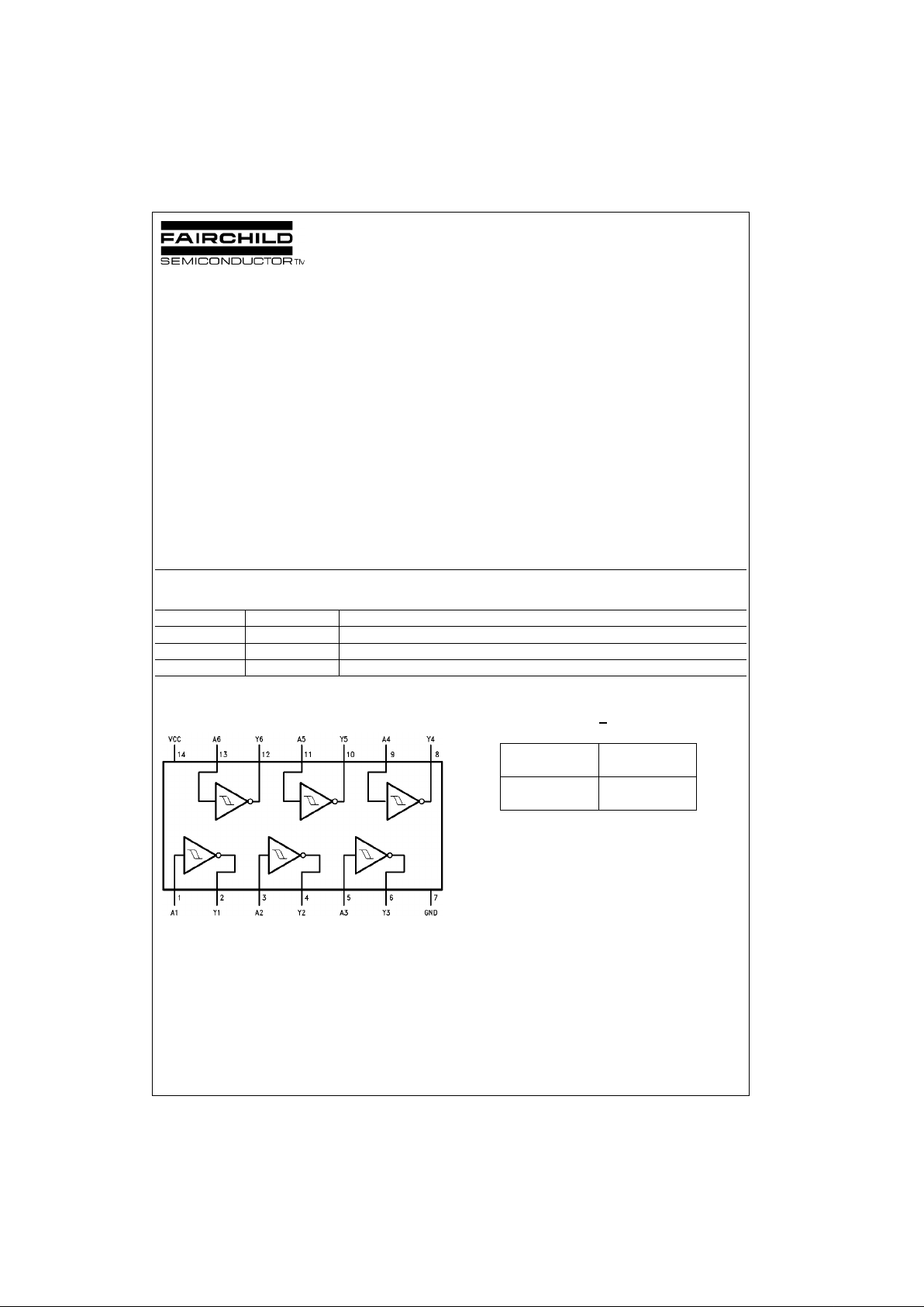
This device contain s six i ndepe ndent gates, each o f whi ch
performs the logic INVERT function. Each input has hysteresis which increases the noise i mmunity and tran sforms a
slowly changing input signal to a fast changin g, jitter-free
output.
Features
■ Input hysteresis
■ Low output noise generation
■ High input noise immunity
■ Switching specification at 50 pF
■ Switching specifications guaranteed over full tempera-
ture and V
CC
range
■ Advanced oxide-isolated, ion-implanted Schottky TTL
process
■ Functionally and pin-for-pin compatible with Schottky
and low power Schottky TTL counterparts
■ Improved AC performance over low power Schottky
counterpart
Ordering Code:
Devices also availab le in Tape and Reel. Specify by appending th e s uffix let t er “X” to the ordering code.
Connection Diagram Function Table
Y = A
H = HIGH Logic Level
L = LOW Logic Level
Order Number Package Number Package Description
DM74ALS14M M14A 14-Lead Small Outline Integrated Circuit (SOIC), JEDEC MS-012, 0.150 Narrow
DM74ALS14SJ M14D 14-Lead Small Outline Package (SOP), EIAJ TYPE II, 5.3mm Wide
DM74ALS14N N14A 14-Lead Plastic Dual-In-Line Package (PDIP), JEDEC MS-001, 0.300 Wide
Input Output
AY
LH
HL
Page 2
www.fairchildsemi.com 2
DM74ALS14
Absolute Maximum Ratings(Note 1)
Note 1: The “Absolute Maximum Ratin gs” are those v alues beyon d which
the safety of the dev ice cannot be guaranteed. T he device sh ould not be
operated at these limits. The parametric values defined in the Electrical
Characteristics tables are not guaranteed at the absolute maximum ratings.
The “Recommend ed O peratin g Cond itions” t able w ill defin e the co ndition s
for actual device operation.
Recommended Operating Conditions
Electrical Characteristics
over recommended free air temperature range (unless otherwise noted)
Note 2: Plastic DIP package.
Note 3: n = number of device outputs, n − 1 outputs switching, each drive n 0V to 3V one output @ GND .
Note 4: n = number of device outputs, n outputs switching, n − 1 inputs switching 0V to 3V. Input under test switching 3V to threshold (V
ILD
); 0V to threshold
(V
IHD
); f = 1 MHz.
Supply Voltage 7V
Input Voltage 7V
Storage Temperature Range −65°C to +150°C
Operating Free Air Temperature Range 0°C to +70°C
Typical θ
JA
N Package 78.5°C/W
M Package 109.0°C/W
Symbol Parameter Min Nom Max Units
V
CC
Supply Voltage 4.5 5 5.5 V
V
T+
Positive-Going Input VCC = Min to Max 1.4 2
V
Threshold Voltage V
CC
= 5V 1.55 1.85
V
T−
Negative-Going Input VCC = Min to Max 0.75 1.2
V
Threshold Voltage V
CC
= 5V 0.85 1.1
HYS Input Hysteresis V
CC
= Min to Max 0.5
V
V
CC
= 5V 0.6
I
OH
HIGH Level Output Current −0.4 mA
I
OL
LOW Level Output Current 8 mA
T
A
Operating Free Air Temperature Range 0 70 °C
Symbol Parameter Test Cond itio ns Min Typ Max Units
V
IK
Input Clamp Voltage VCC = Min, II = −18 mA −1.5 V
V
OH
HIGH Level Output Voltage VCC = 4.5V to 5.5V, IOH = Max VCC − 2V
V
OL
LOW Level Output Voltage VCC = Min IOL = 4 mA 0.25 0.4 V
IOL = 8 mA 0.35 0.5 V
I
T+
Input Current at Positive-Going Threshold Voltage VCC = 5V, VI = V
T+
20 µA
I
T−
Input Current at Negative-Going Threshold Voltage VCC = 5V, VI = V
T−
−100 µA
I
I
Input Current at Maximum Input Voltage VCC = Max, VI = 7V 100 µA
I
IH
HIGH Level Input Current VCC = Max, VI = 2.7V 20 µA
I
IL
LOW Level Input Current VCC = Max, VI = 0.4V −100 µA
I
O
Output Drive Current VCC = Max, VO = 2.25V −30 −112 mA
I
CCH
Supply Current with Outputs HIGH VCC = Max 12 mA
I
CCL
Supply Current with Outputs LOW VCC = Max 12 mA
V
OLP
Quiet Output Maximum VCC = 5.0V, TA = 25°C
0.16 V
Dynamic V
OL
(Figures 1, 2); (Note 2)(Note 3)
V
OLV
Quiet Output Minimum VCC = 5.0V, TA = 25°C
−0.27 V
Dynamic V
OL
(Figures 1, 2); (Note 2)(Note 3)
V
IHD
Minimum HIGH Level VCC = 5.0V, TA = 25°C
1.44 V
Dynamic Input Voltage (Note 2)(Note 4)
V
ILD
Maximum LOW Level VCC = 5.0V, TA = 25°C
1.15 V
Dynamic Input Voltage (Note 2)(Note 4)
Page 3

3 www.fairchildsemi.com
DM74ALS14
Switching Characteristics over recommended operating free air temperature range
ALS Noise Characteristics
The setup of a noise characteristics measurement is critical
to the accuracy and repeatability of the tests. The following
is a brief description of the setup used to measure the
noise characteristics of ALS.
Equipment:
Word Generator
Printed Circuit Board Test Fixture Dual Trace Oscillo-
scope
Procedure:
1. Verify Test Fixture Loading: Standard Load 50 pF,
500Ω.
2. Deskew the word generat or so that no two channels
have greater than 150 ps skew between them. This
requires that the oscilloscope be deskewed first. Swap
out the channels that have more than 150 ps of skew
until all channels being used a re within 150 ps. It is
important to deskew the word generator channels
before testing. This will ensure that the outputs switch
simultaneously.
3. Terminate all inputs and outputs to ensure proper loading of the outputs and that the input levels are at the
correct voltage.
4. Set V
CC
to 5.0V.
5. Set the word generat or to toggle all but one out put a t a
frequency of 1 MHz. Greater frequencies will increase
DUT heating and affect the results of the measurement.
6. Set the word generator input lev els at 0V LO W and 3V
HIGH. Verify levels with a digital volt meter.
V
OLP/VOLV
and V
OHP/VOHV
:
• Determine the quiet output pin that demonstrates the
greatest noise levels. The worst case pin will usually be
the furthest from the gr oun d p in. Monitor the output volt ages using a 50Ω coaxial cable plugged into a standard
SMB type connector o n the test fixture. Do not use an
active FET probe.
• Verify that the GND reference recorded on the oscilloscope has not drifted to ensure the accuracy and repeatability of the measurements.
V
ILD
and V
IHD
:
• Monitor one of the switching outputs using a 50Ω coaxial
cable plugged into a st andard SMB type connector on
the test fixture. Do not use an active FET probe.
• First increase the input LOW voltage level, V
IL
, until the
output begins to oscillate. Oscillation is defined as noise
on the output LOW lev el that exceeds V
IL
limits, or on
output HIGH levels that exceed V
IH
limits. The input
LOW voltage level at which oscillation occurs is defined
as V
ILD
.
• Next decrease the input HIGH voltage level on the word
generator, V
IH
until the output begins to oscillate. Oscil-
lation is defined as noise on the output LOW leve l that
exceeds V
IL
limits, or on output HIGH levels that exceed
V
IH
limits. The input HIGH voltage level at which oscilla-
tion occurs is defined as V
IHD
.
• Verify that the GND reference recorded on the oscilloscope has not drifted to ensure the accuracy and repeatability of the measurements.
V
OHV
and V
OHP
are measured wit h respect to VOH reference. V
OLV
and
V
OLP
are measured with re s pect to ground referenc e.
Input pulses ha ve the following characteristic s: f = 1 MHz, t
r
= 3 ns, tf =
3 ns, skew < 150 ps.
FIGURE 1. Quiet Output Noise Voltage Waveforms
FIGURE 2. Simultaneous Switching Test Circuit
Symbol Parameter Conditions Min Max Units
t
PLH
Propagation Delay Time LOW-to-HIGH Level Output VCC = 4.5V to 5.5V 2 12 ns
t
PHL
Propagation Delay Time HIGH-to-LOW Level Output RL = 500Ω, CL = 50 pF 2 10 ns
Page 4

www.fairchildsemi.com 4
DM74ALS14
Physical Dimensions inches (millimeters) unless otherwise noted
14-Lead Small Outline Integrated Circuit (SOIC), JEDEC MS-012, 0.150 Narrow
Package Number M14A
Page 5

5 www.fairchildsemi.com
DM74ALS14
Physical Dimensions inches (millimeters) unless otherwise noted (Continued)
14-Lead Small Outline Package (SOP), EIAJ TYPE II, 5.3mm Wide
Package Number M14D
Page 6

www.fairchildsemi.com 6
DM74ALS14 Hex Inverter with Schmitt Trigger Inputs
Physical Dimensions inches (millimeters) unless otherwise noted (Continued)
14-Lead Plastic Dual-In-Line Package (PDIP), JEDEC MS-001, 0.300 Wide
Package Number N14A
Fairchild does not assume any responsibility for use of any circuitry described, no circuit pate nt licenses are implied and
Fairchild reserves the right at any time without notice to change said circuitry and specifications.
LIFE SUPPORT POLICY
FAIRCHILD’S PRODUCTS ARE NOT AUTHORIZED FOR USE AS CRITICAL COMPONENTS IN LIFE SUPPORT
DEVICES OR SYSTEMS WITHOUT THE EXPRESS WRITTEN APPROVAL OF THE PRESIDENT OF FAIRCHILD
SEMICONDUCTOR CORPORATION. As used herein:
1. Life support devices or syste ms a re device s or syste ms
which, (a) are intended for surgical implant into the
body, or (b) support or sustain life, and (c) whose failure
to perform when properly used in accordance with
instructions for use provided in the labeling, can be reasonably expected to result in a significant inju ry to the
user.
2. A critical compon ent in any com ponen t of a life su pport
device or system whose failu re to perform can be reasonably expected to ca use the fa i lure of the life su pp ort
device or system, or to affect its safety or effectiveness.
www.fairchildsemi.com
 Loading...