

Datasheet DM74ALS138SJX, DM74ALS138SJ, DM74ALS138N, DM74ALS138MX, DM74ALS138M Datasheet (Fairchild Semiconductor)
Page 1
© 2000 Fairchild Semiconductor Corporation DS006111 www.fairchildsemi.com
September 1986
Revised February 2000
DM74ALS138 3 to 8 Line Decoder/Demultiplexer
DM74ALS138
3 to 8 Line Decoder/Demultiplexer
General Description
These Schottky-clamped circuits are designed to be used
in high-performance memory-decoding or data-routing
applications, requiring very short propagatio n delay times.
In high-performance memo ry systems these decoders can
be used to minimize the effects of system decoding. When
used with high-speed me mories, the delay tim es of these
decoders are usually less th an the typical access time of
the memory. This means that the effective system delay
introduced by the decoder is negligible.
The DM74ALS138 decodes one-of-eight lines, based upon
the conditions at the three binary select inputs and the
three enable inputs. Two active-LOW and one active-HIGH
enable inputs reduce the need fo r external gate s or inverters when expanding. A 24-line decoder can be implemented with no external inverters, and 32-line decoder
requires only one inverter. An enable input can be used as
a data input for demultiplexing applications.
This decoder/demul tiplexer features fully buffered inputs,
presenting only one normalized load to its driving circuit. All
inputs are clamped wit h hig h-p er for man ce Sc h ottk y diod es
to suppress line-ringing and simplify system design.
Features
■ Designed specifically for high speed:
Memory decoders
Data transmission systems
■ 3- to 8-line decoder inco rpo ra tes 3 enable inputs to sim-
plify cascading and/or data reception
■ Low power dissipation…23 mW typ
■ Switching specifications guaranteed over full tempera-
ture and V
CC
range
■ Advanced oxide-isolated, ion-implanted Schottky TTL
process
Ordering Code:
Devices also availab le in Tape and Reel. Specify by appending th e s uffix let t er “X” to the ordering code.
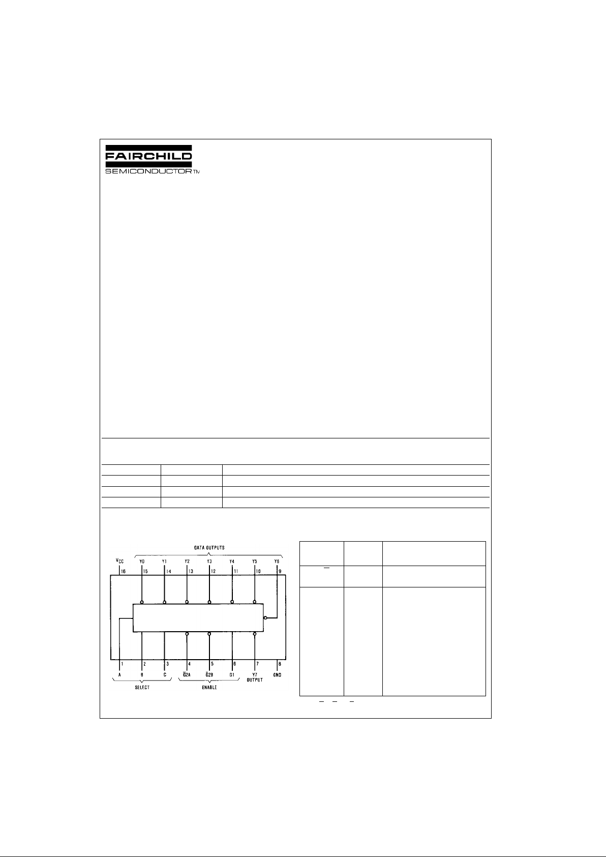
Connection Diagram Function Table
Note 1: G2 = G2A + G2B
Order Number Package Number Package Description
DM74ALS138M M16A 16-Lead Small Outline Integrated Circuit (SOIC), JEDEC MS-012, 0.150 Narrow
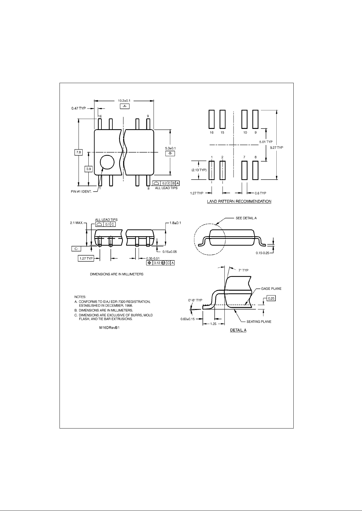
DM74ALS138SJ M16D 16-Lead Small Outline Package (SOP), EIAJ TYPE II, 5.3mm Wide
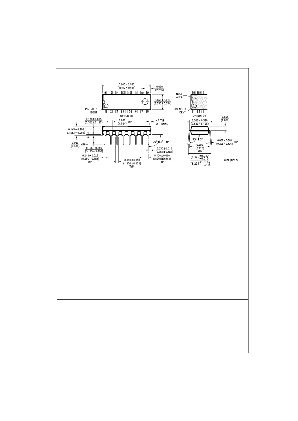
DM74ALS138N N16E 16-Lead Plastic Dual-In-Line Package (PDIP), JEDEC MS-001, 0.300 Wide
Enable Select
Outputs
Inputs Inputs
G1 G
2
(Note 1)
C B AY0Y1Y2Y3Y4Y5Y6Y7
X H XXXHHHHHHHH
L X XXXHHHHHHHH
H L L LL LHHHHHHH
H L L LHHLHHHHHH
H L LHLHHLHHHHH
H L LHHHHHLHHHH
H L HLLHHHHLHHH
H L HLHHHHHHLHH
H L HHLHHHHHHLH
H L HHHHHHHHHHL
Page 2
www.fairchildsemi.com 2
DM74ALS138
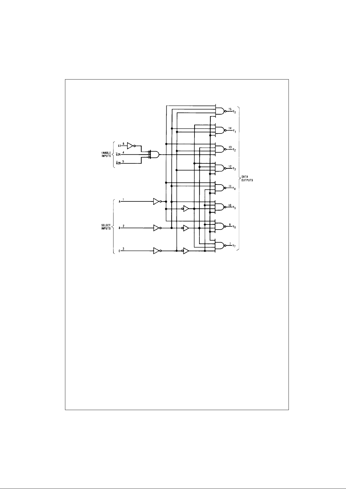
Logic Diagram
Page 3
3 www.fairchildsemi.com
DM74ALS138
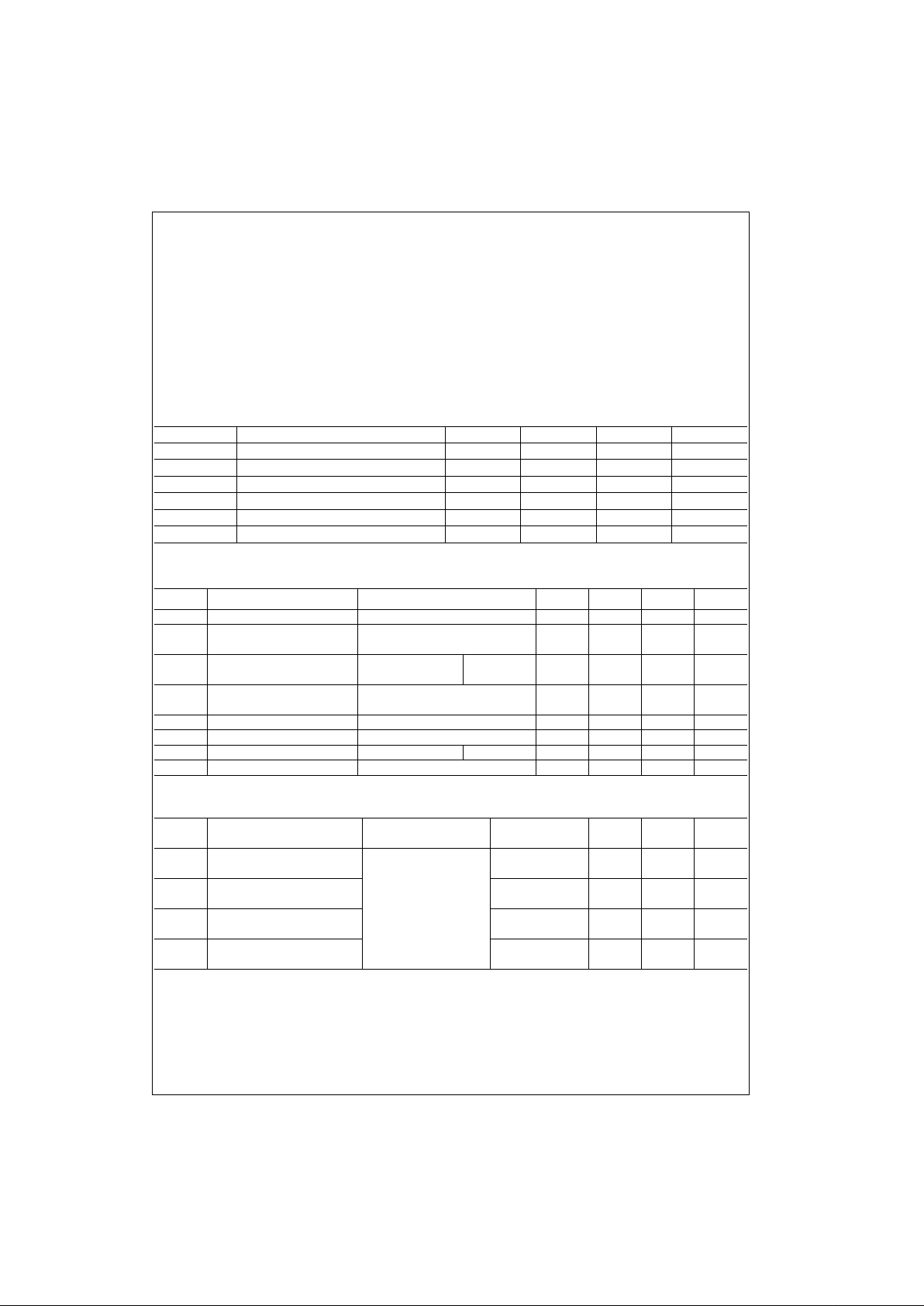
Absolute Maximum Ratings(Note 2)
Note 2: The “Absolute M aximu m R atin gs” are t hose valu es b eyo nd w hich
the safety of the device cannot be guaranteed. The device should not be
operated at these limits. The parametric values defined in the Electrical
Characteristics tables are not guaranteed at the absolute maximum ratings.
The “Recommend ed O peratin g Cond itions” t able w ill defin e the condition s
for actual device operation.
Recommended Operating Conditions
Electrical Characteristics
over recommended operating free air temperature range. All typical values are measured at VCC = 5V, TA = 25°C.
Switching Characteristics
over recommended operating free air temperature range.
Supply Voltage 7V
Input Voltage 7V
Operating Free Air Temperature Range 0°C to +70°C
Storage Temperature Range −65°C to +150°C
Typical θ
JA
N Package 75.5°C/W
M Package 104.0°C/W
Symbol Parameter Min Nom Max Units
V
CC
Supply Voltage 4.5 5 5.5 V
V
IH
HIGH Level Input Voltage 2 V
V
IL
LOW Level Input Voltage 0.8 V
I
OH
HIGH Level Output Current −0.4 mA
I
OL
LOW Level Output Current 8 mA
T
A
Free Air Operating Temperature 0 70 °C
Symbol Parameter Conditions Min Typ Max Units
V
IK
Input Clamp Voltage VCC = 4.5V, II = −18 mA −1.5 V
V
OH
HIGH Level IOH = −0.4 mA VCC − 2V
Output Voltage VCC = 4.5V to 5.5V
V
OL
LOW Level
VCC = 4.5V IOL = 8 mA 0.35 0.5 V
Output Voltage
I
I
Input Current @ Max.
VCC = 5.5V, VIH = 7V 0.1 mA
Input Voltage
I
IH
HIGH Level Input Current VCC = 5.5V, VIH = 2.7V 20 µA
I
IL
LOW Level Input Current VCC = 5.5V, VIL = 0.4V −0.1 mA
I
O
Output Drive Current VCC = 5.5V VO = 2.25V −30 −112 mA
I
CC
Supply Current VCC = 5.5V 5 10 mA
Symbol Parameter Conditions
From (Input)
Min
Max
Units
To (Outpu t)
t
PLH
Propagation Delay Time VCC = 4.5V to 5.5V A, B, C
622ns
LOW-to-HIGH Level Output RL = 500Ω to Y
t
PHL
Propagation Delay Time CL = 50 pF A, B, C
618ns
HIGH-to-LOW Level Output to Y
t
PLH
Propagation Delay Time Enable
417ns
LOW-to-HIGH Level Output to Y
t
PHL
Propagation Delay Time Enable
517ns
HIGH-to-LOW Level Output to Y
Page 4
www.fairchildsemi.com 4
DM74ALS138
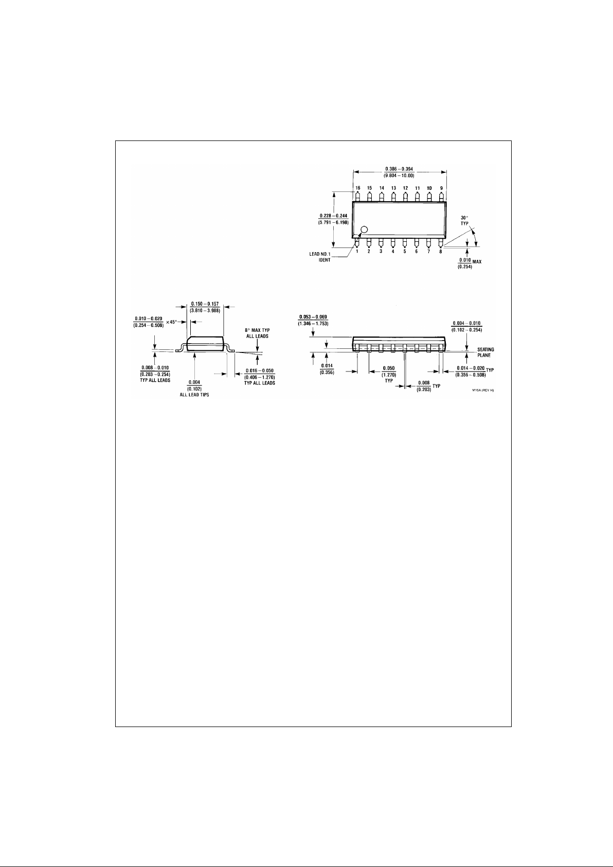
Physical Dimensions inches (millimeters) unless otherwise noted
16-Lead Small Outline Integrated Circuit (SOIC), JEDEC MS-012, 0.150 Narrow
Package Number M16A
Page 5
5 www.fairchildsemi.com
DM74ALS138
Physical Dimensions inches (millimeters) unless otherwise noted (Continued)
16-Lead Small Outline Package (SOP), EIAJ TYPE II, 5.3mm Wide
Package Number M16D
Page 6
www.fairchildsemi.com 6
DM74ALS138 3 to 8 Line Decoder/Demultiplexer
Physical Dimensions inches (millimeters) unless otherwise noted (Continued)
16-Lead Plastic Dual-In-Line Package (PDIP), JEDEC MS-001, 0.300 Wide
Package Number N16E
Fairchild does not assume any responsibility for use of any circuitry described, no circuit pate nt licenses are implied and
Fairchild reserves the right at any time without notice to change said circuitry and specifications.
LIFE SUPPORT POLICY
FAIRCHILD’S PRODUCTS ARE NOT AUTHORIZED FOR USE AS CRITICAL COMPONENTS IN LIFE SUPPORT
DEVICES OR SYSTEMS WITHOUT THE EXPRESS WRITTEN APPROVAL OF THE PRESIDENT OF FAIRCHILD
SEMICONDUCTOR CORPORATION. As used herein:
1. Life support devices or systems are devices or syste ms
which, (a) are intended for surgical implant into the
body, or (b) support or sustain life, and (c) whose failure
to perform when properly used in accordance with
instructions for use provided in the labeling, can be reasonably expected to result in a significant inju ry to the
user.
2. A critical component i n any compon ent of a lif e support
device or system whose failu re to perform can be reasonably expected to ca use the fa i lure of the life su pp ort
device or system, or to affect its safety or effectiveness.
www.fairchildsemi.com
 Loading...