

Page 1
© 2000 Fairchild Semiconductor Corporation DS006261 www.fairchildsemi.com
September 1986
Revised February 2000
DM74ALS1240A Octal 3-STATE Bus Driver
DM74ALS1240A
Octal 3-STATE Bus Driver
General Description
These octal 3-STATE bus drivers are designed to provide
the designer with flexibility in implementing a bus interface
with memory, microprocessor, or communication systems,
and are low power dissipation versions of the
DM74ALS240A and DM74ALS241A. The output 3-STATE
gating control is organized into two separate groups of four
buffers. The DM74ALS1240A control inputs symmetrically
enable the respective outp uts when set l ogic LOW. The 3STATE circuitry contains a feature that maintains the buffer
outputs in 3-STATE (high impedance state) during pow er
supply ramp-up or ramp-d own. This eliminates bus gli tching problems that arise during power-up and power-down.
Features
■ Advanced oxide-isolated, ion-implanted Schottky TTL
process
■ Switching response specified into 500Ω and 50 pF load
■ Switching response specific ations guaranteed over full
temperat ure and V
CC
supply range
■ PNP input design reduces input loading
■ Low power dissipation version
■ Low level drive current: 74ALS = 16 mA
Ordering Code:
Devices also availab le in Tape and Reel. Specify by appending th e s uffix let t er “X” to the ordering code.
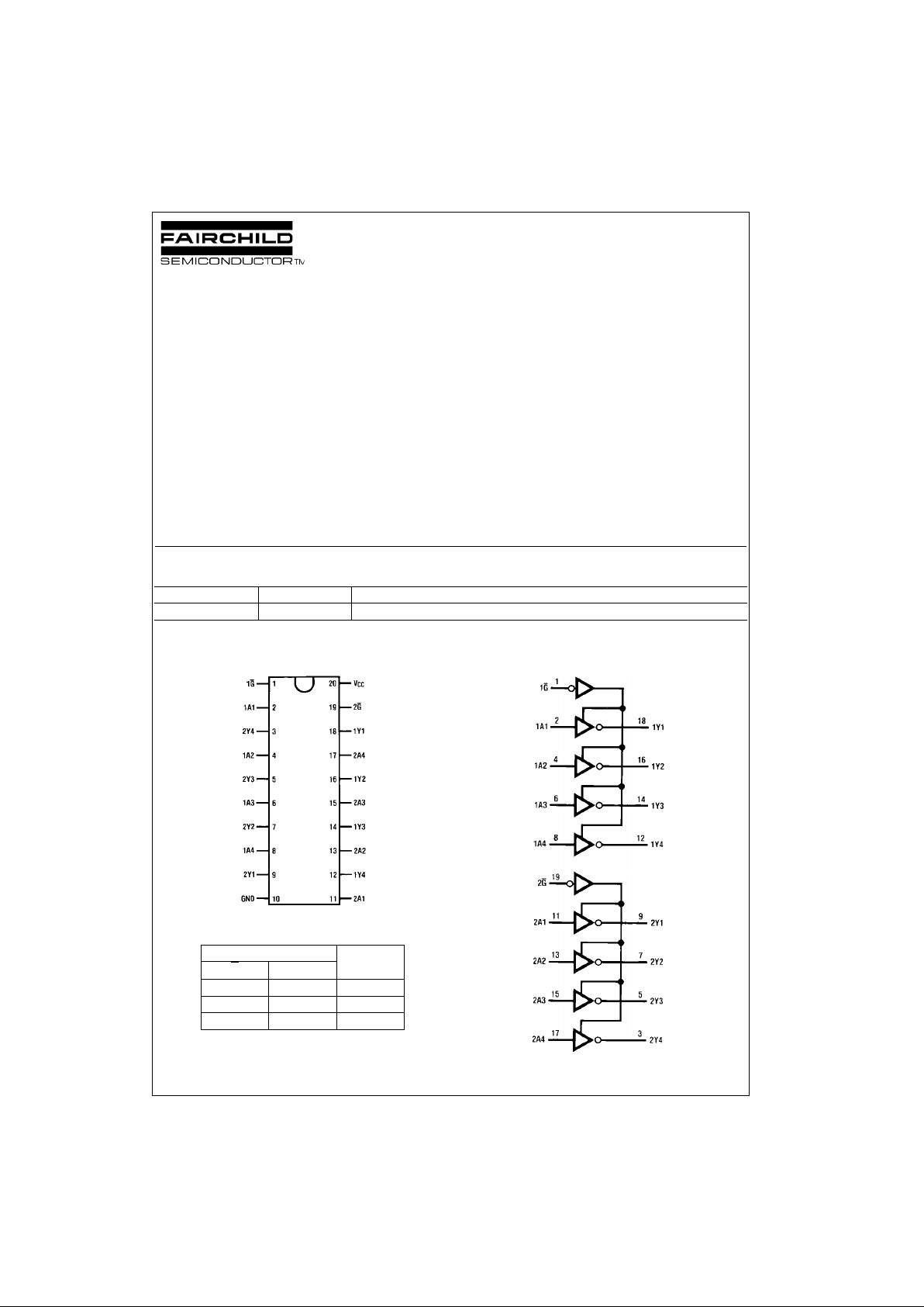
Connection Diagram
Function Table
H = HIGH Level Logic State
L = LOW Level Logic State
X = Don't Care (Either LOW or HIGH Level Logic State)
Z = High Impedance (OFF) State
Logic Diagram
Order Number Package Number Package Description
DM74ALS1240AWM M20B 20-Lead Small Outline Integrated Circuit (SOIC), JEDEC MS-013, 0.300 Wide
Input Output
G
AY
LLH
LHL
HXZ
Page 2
www.fairchildsemi.com 2
DM74ALS1240A
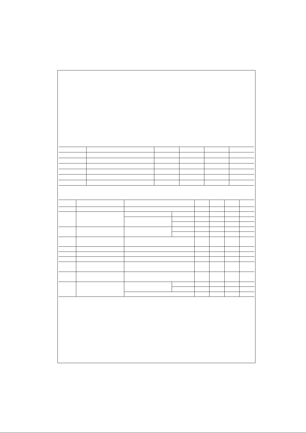
Absolute Maximum Ratings(Note 1)
Note 1: The “Absolute Maximum Ratings” are those values beyond which
the safety of the dev ice cannot be guaranteed. T he device sh ould not be
operated at these limits. The parametric values defined in the Electrical
Characteristics tables are not guaranteed at the absolute maximum ratings.
The “Recommend ed O peratin g Cond itions” t able w ill defin e the co ndition s
for actual device operation.
Recommended Operating Conditions
Electrical Characteristics
over recommended operating free air temperature range (unless otherwise specified)
Supply Voltage 7V
Input Voltage 7V
Voltage Applied to Disabled Output 5.5V
Operating Free Air Temperature Range 0°C to +70°C
Storage Temperature Range −65°C to +150°C
Typical θ
JA
N Package 60.5°C/W
M Package 78.0°C/W
Symbol Parameter Min Typ Max Units
V
CC
Supply Voltage 4.5 5 5.5 V
V
IH
HIGH Level Input Voltage 2 V
V
IL
LOW Level Input Voltage 0.8 V
I
OH
HIGH Level Output Current −15 mA
I
OL
LOW Level Output Current 16 mA
T
A
Operating Free Air Temperature 0 70 °C
Symbol Parameter Conditions Min Typ Max Units
V
IK
Input Clamp Voltage VCC = 4.5V, II = −18 mA −1.2 V
V
OH
HIGH Level VCC = 4.5V to 5.5V IOH = −0.4 mA VCC − 2V
Output Voltage VCC = 4.5V IOH = −3 mA 2.4 V
IOH = Max 2 V
V
OL
LOW Level VCC = 4.5V IOL = 12 mA 0.25 0.4 V
Output Voltage IOL = 24 mA 0.35 0.5 V
I
I
Input Current at Maximum
VCC = 5.5V, VI = 7V 0.1 mA
Input Voltage
I
IH
HIGH Level Input Current VCC = 5.5V, VI = 2.7V 20 µA
I
IL
LOW Level Input Current VCC = 5.5V, VIL = 0.4V −0.1 mA
I
O
Output Drive Current VCC = 5.5V, VO = 2.25V −30 −112 mA
I
OZH
HIGH Level 3-STATE
VCC = 5.5V, VO = 2.7V 20 µA
Output Current
I
OZL
LOW Level 3-STATE
VCC = 5.5V, VO = 0.4V −20 µA
Output Current
I
CC
Supply Current
VCC = 5.5V
Outputs HIGH 5 8 mA
Outputs LOW 8 14 mA
Outputs 3-STATE 8 13 mA
Page 3

3 www.fairchildsemi.com
DM74ALS1240A
Switching Characteristics
over recommended operating free air temperature range
Symbol Parameter
VCC = 4.5V to 5.5V, CL = 50 pF,
Units
From To R1 = 500Ω, R2 = 500Ω,
(Input) (Output)
TA = Min to Max
Min Max
t
PLH
Propagation Delay Time
213ns
LOW-to-HIGH Level Output
AY
t
PHL
Propagation Delay Time
213ns
HIGH-to-LOW Level Output
t
PZH
Output Enable Time
420ns
to HIGH Level Output
G Y
t
PZL
Output Enable Time
622ns
to LOW Level Output
t
PHZ
Output Disable Time
210ns
from HIGH Level Output
G Y
t
PLZ
Output Disable Time
313ns
from LOW Level Output
Page 4

www.fairchildsemi.com 4
DM74ALS1240A Octal 3-STATE Bus Driver
Physical Dimensions inches (millimeters) unless otherwise noted
20-Lead Small Outline Integrated Circuit (SOIC), JEDEC MS-013, 0.300 Wide
Package Number M20B
Fairchild does not assume any responsibility for use of any circuitry described, no circuit pate nt licenses are implied and
Fairchild reserves the right at any time without notice to change said circuitry and specifications.
LIFE SUPPORT POLICY
FAIRCHILD’S PRODUCTS ARE NOT AUTHORIZED FOR USE AS CRITICAL COMPONENTS IN LIFE SUPPORT
DEVICES OR SYSTEMS WITHOUT THE EXPRESS WRITTEN APPROVAL OF THE PRESIDENT OF FAIRCHILD
SEMICONDUCTOR CORPORATION. As used herein:
1. Life support devices or systems are devices or syste ms
which, (a) are intended for surgical implant into the
body, or (b) support or sustain life, and (c) whose failure
to perform when properly used in accordance with
instructions for use provided in the labeling, can be reasonably expected to result in a significant inju ry to the
user.
2. A critical component i n any compon ent of a lif e support
device or system whose failu re to perform can be reasonably expected to ca use the fa i lure of the life su pp ort
device or system, or to affect its safety or effectiveness.
www.fairchildsemi.com
 Loading...