

Page 1
查询DM74157供应商
DM74157
Quad 2-Line to 1-Line Data Selectors/Multiplexer
DM74157 Quad 2-Line to 1-Line Data Selectors/Multiplexer
August 1986
Revised February 2000
General Description
These data selectors/multiplexers contain inverters and
drivers to supply full on-chip da ta selection to the fo ur output gates. A separate strobe input is provided. A 4-bit word
is selected from one o f two sources and is route d to the
four outputs.
Applications
• Expand any data input point
• Multiplex dual data buses
• Generate four fun ction s of tw o va riab l es ( on e v aria ble i s
common)
• Source programmable counters
Features
■ Buffered inputs and outputs
■ Typical propagation time 9 ns
■ Typical powe r dissipation 150 mW
Ordering Code:
Order Number Package Number Package Description
DM74157N N16E 16-Lead Plastic Dual-In-Line Package (PDIP), JEDEC MS-001, 0.300 Wide
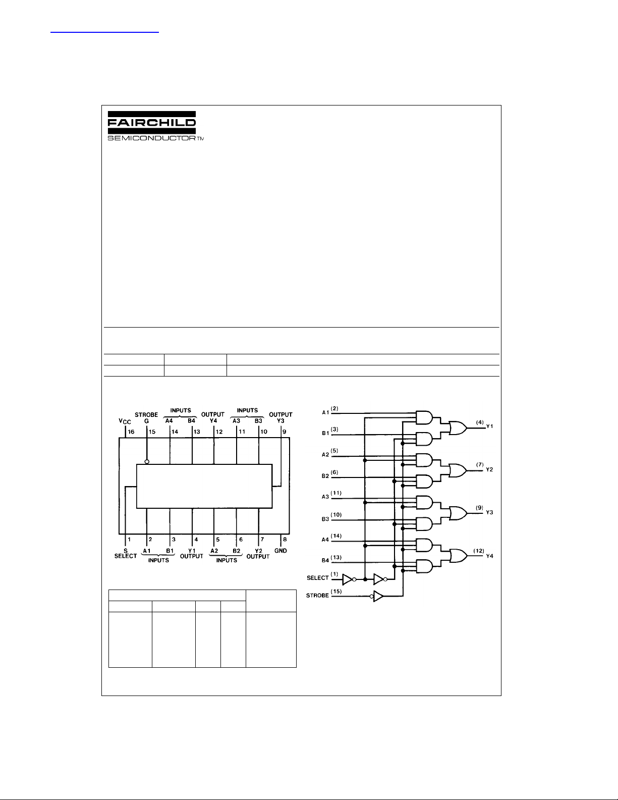
Connection Diagram
Logic Diagram
Function Table
Inputs
Strobe Select A B
HXXXL
LLLXL
LLHXH
LHXLL
LHXHH
H = HIGH Level, L = LOW Level, X = Don’t Care
© 2000 Fairchild Semiconductor Corporation DS006550 www.fairchildsemi.com
Output Y
Page 2
Absolute Maximum Ratings(Note 1)
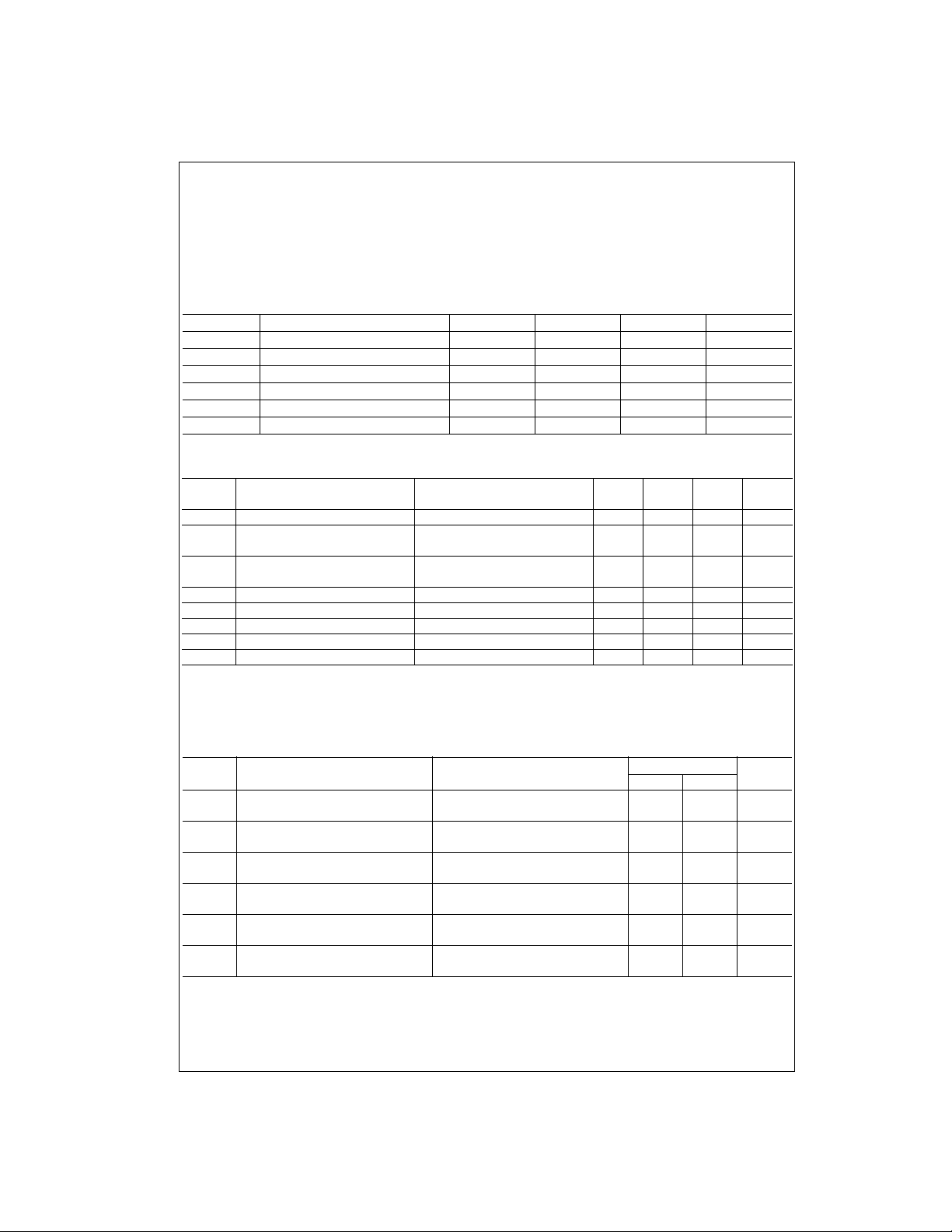
Supply Voltage 7V
Input Voltage 5.5V
DM74157
Operating Free Air Temperature Range 0°C to +70°C
Note 1: The “Absolute Maximum Ratin gs” are those v alues beyon d which
the safety of the dev ice cannot be guaranteed. T he device sh ould not be
operated at these limits. The parametric values defined in the Electrical
Characteristics tables are not guaranteed at the absolute maximum ratings.
The “Recommend ed O peratin g Cond itions” t able w ill defin e the c ondit ions
for actual device operation.
Storage Temperature Range −65°C to +150°C
Recommended Operating Conditions
Symbol Parameter Min Nom Max Units
V
CC
V
IH
V
IL
I
OH
I
OL
T
A
Supply Voltage 4.75 5 5.25 V
HIGH Level Input Voltage 2 V
LOW Level In put Voltage 0.8 V
HIGH Level Output Current −0.8 mA
LOW Level Output Current 16 mA
Free Air Operating Temperature 0 70 °C
Electrical Characteristics
over recommended operating free air temperature range (unless otherwise noted)
Symbol Parameter Conditions Min
V
I
V
OH
V
OL
I
I
I
IH
I
IL
I
OS
I
CC
Note 2: All typicals are at VCC = 5V, TA = 25°C.
Note 3: Not more than one output should be shorted at a time.
Note 4: I
Input Clamp Voltage VCC = Min, II = −12 mA −1.5 V
HIGH Level VCC = Min, IOH = Max
Output Voltage VIL = Max, VIH = Min
LOW Level VCC = Min, IOL = Max
Output Voltage VIH = Min, VIL = Max
Input Current @ Max Input Voltage VCC = Max, VI = 5.5V 1 mA
HIGH Level Input Current VCC = Max, VI = 2.4V 40 µA
LOW Level Input Current VCC = Max, VI = 0.4V −1.6 mA
Short Circuit Output Current VCC = Max (Note 3) −18 −55 mA
Supply Current VCC = Max (Note 4) 30 48 mA
is measured with 4.5V applied to all inputs and all outputs OPEN.
CC
2.4 3.4 V
Typ
(Note 2)
Max Units
0.4 V
Switching Characteristics
at VCC = 5V and TA = 25°C
Symbol Parameter
t
PLH
t
PHL
t
PLH
t
PHL
t
PLH
t
PHL
www.fairchildsemi.com 2
Propagation Delay Time
LOW-to-HIGH Level Output
Propagation Delay Time
HIGH-to-LOW Level Output
Propagation Delay Time
LOW-to-HIGH Level Output
Propagation Delay Time
HIGH-to-LOW Level Output
Propagation Delay Time
LOW-to-HIGH Level Output
Propagation Delay Time
HIGH-to-LOW Level Output
From (Input) RL = 400Ω, CL = 15 pF
To (Output) Min Max
Data to Y 14 ns
Data to Y 14 ns
Strobe to Y 20 ns
Strobe to Y 21 ns
Select to Y 23 ns
Select to Y 27 ns
Units
Page 3
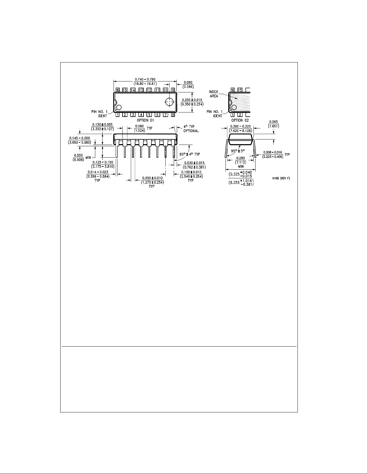
Physical Dimensions inches (millimeters) unless otherwise noted
DM74157 Quad 2-Line to 1-Line Data Selectors/Multiplexer
16-Lead Plastic Dual-In-Line Package (PDIP), JEDEC MS-001, 0.300 Wide
Fairchild does not assume any responsibility for use of any circuitry described, no circuit patent license s are implied and
Fairchild reserves the right at any time without notice to change said circuitry and specifications.
LIFE SUPPORT POLICY
FAIRCHILD’S PRODUCTS ARE NOT AUTHORIZED FOR USE AS CRITICAL COMPONENTS IN LIFE SUPPORT
DEVICES OR SYSTEMS WITHOUT THE EXPRESS WRITTEN APPROVAL OF THE PRESIDENT OF FAIRCHILD
SEMICONDUCTOR CORPORATION. As used herein:
1. Life support devices or systems are devices or systems
which, (a) are intended for surgical implant into the
body, or (b) support or sustain life, and (c) whose failure
to perform when properly used in accordance with
instructions for use provide d in the labe l ing, can be re asonably expected to result in a significant injury to the
user.
Package Number N16E
2. A critical componen t in any com ponen t of a life s upport
device or system whose failu re to perform can b e reasonably expected to cause the failure of the life support
device or system, or to affect its safety or effectiveness.
www.fairchildsemi.com
3 www.fairchildsemi.com
 Loading...