

Page 1

PIC32MM0256GPM064 FAMILY
32-Bit Flash Microcontroller with MIPS32® microAptiv™ UC Core,
Low Power and USB
Operating Conditions
• 2.0V to 3.6V, -40ºC to +125ºC, DC to 25 MHz
Low-Power Modes
• Low-Power modes:
- Idle – CPU off, peripherals run from system clock
- Sleep – CPU and peripherals off:
- Fast wake-up Sleep with retention
- Low-power Sleep with retention
•0.65 μA Sleep current for RAM Retention
Regulator mode and 5 μA for Regulator Standby mode
• On-Chip 1.8V Voltage Regulator (VREG)
• On-Chip Ultra Low-Power Retention Regulator
High-Performance 32-Bit RISC CPU
• microAptiv™ UC 32-Bit Core with 5-Stage Pipeline
• microMIPS™ Instruction Set for 35% Smaller Code and
98% Performance compared to MIPS32 Instructions
• 1.53 DMIPS/MHz (37 DMIPS) (Dhrystone 2.1) Performance
• 3.17 CoreMark®/MHz (79 CoreMark) Performance
• 16-Bit/32-Bit Wide Instructions with 32-Bit Wide Data Path
• Two Sets of 32 Core Register Files (32-bit) to Reduce
Interrupt Latency
• Single-Cycle 32x16 Multiply and Two-Cycle 32x32 Multiply
• 64-Bit, Zero Wait State Flash with ECC to Maximize
Endurance/Retention
Microcontroller Features
• Up to 256K Flash Memory:
- 20,000 erase/write cycle endurance
- 20 years minimum data retention
- Self-programmable under software control
• Up to 32K SRAM Memory
• Multiple Interrupt Vectors with Individually
Programmable Priority
• Fail-Safe Clock Monitor mode
• Configurable Watchdog Timer with On-Chip, Low-Power
RC Oscillator
• Programmable Code Protection
• Selectable Oscillator Options Including:
- High-precision, 8 MHz Internal RC (FRC)
Oscillator – 2x/3x/4x/6x/12x/24x PLL, which can be
clocked from FRC or the Primary Oscillator
- Primary high-speed, crystal/resonator oscillator or
external clock
Peripheral Features
• USB 2.0 Compliant Full-Speed and Low-Speed Device,
Host and On-The-Go (OTG) Controller:
- Dedicated DMA
- Device mode operation from FRC oscillator;
no crystal oscillator required
• Atomic Set, Clear and Invert Operation on Select
Peripheral Registers
• High-Current Sink/Source
• Independent, Low-Power 32 kHz Timer Oscillator
• Three 4-Wire SPI modules:
- 16-byte FIFO
- Variable width
- I2S mode
• Three I2C Master and Slave w/Address Masking and
IPMI Support
• Three Enhanced Addressable UARTs:
- RS-232, RS-485 and LIN/J2602 support
- IrDA® with on-chip hardware encoder and decoder
• External Edge and Level Change Interrupt on All Ports
• Hardware Real-Time Clock and Calendar (RTCC)
• Up to 24 Peripheral Pin Select (PPS) Remappable Pins
• 21 Total 16-Bit Timers:
- Three dedicated 16-bit timers/counters
- Two can be concatenated to form a 32-bit timer
- Two additional 16-bit timers in each MCCP and
SCCP module, totaling 18
• Capture/Compare/PWM/Timer modules:
- Two 16-bit timers or one 32-bit timer in each module
- PWM resolution down to 21 ns
- Three Multiple Output (MCCP) modules:
- Flexible configuration as PWM, input capture,
output compare or timers
- Six PWM outputs
- Programmable dead time
- Auto-shutdown
- Six Single Output (SCCP) modules:
- Flexible configuration as PWM, input capture,
output compare or timers
- Single PWM output
• Reference Clock Output (REFO)
• Four Configurable Logic Cells (CLCs) with Internal
Connections to Select Peripherals and PPS
• Four-Channel Hardware DMA with Automatic Data Size
Detection and CRC Engine
Debug Features
• Two Programming and Debugging Interfaces:
- Two-wire ICSP™ interface with non-intrusive access
and real-time data exchange with application
- Four-wire MIPS® standard Enhanced JTAG interface
• IEEE Standard 1149.2 Compatible (JTAG) Boundary Scan
2016-2019 Microchip Technology Inc. DS60001387D-page 1
Page 2

PIC32MM0256GPM064 FAMILY
Analog Features
• Three Analog Comparators with Input Multiplexing
• Programmable High/Low-Voltage Detect (HLVD)
• 5-Bit Comparator Voltage Reference DAC with Pin Output
• Up to 24-Channel, Software-Selectable 10/12-Bit SAR
Analog-to-Digital Converter (ADC):
- 12-bit 200K samples/second conversion rate
(single Sample-and-Hold)
- 10-bit 300k samples/second conversion rate
(single Sample-and-Hold)
- Sleep mode operation
- Low-voltage boost for input
- Band gap reference input feature
- Windowed threshold compare feature
- Auto-scan feature
• Brown-out Reset (BOR)
TABLE 1: PIC32MM0256GPM064 FAMILY DEVICES
Remappable
Peripherals
Device
PIC32MM0064GPM028 28 64 16 21/18 21 18 3 3 3 6 4 3 12 3 Yes Yes 3 Yes SSOP/QFN/
PIC32MM0128GPM028 28 128 16 21/18 21 18 3 3 3 6 4 3 12 3 Yes Yes 3 Yes SSOP/QFN/
PIC32MM0256GPM028 28 256 32 21/18 21 18 3 3 3 6 4 3 12 3 Yes Yes 3 Yes SSOP/QFN/
PIC32MM0064GPM036 36/40 64 16 27/20 21 20 3 3 3 6 4 3 15 3 Yes Yes 3 Yes VQFN/UQFN
PIC32MM0128GPM036 36/40 128 16 27/20 21 20 3 3 3 6 4 3 15 3 Yes Yes 3 Yes VQFN/UQFN
PIC32MM0256GPM036 36/40 256 32 27/20 21 20 3 3 3 6 4 3 15 3 Yes Yes 3 Yes VQFN/UQFN
PIC32MM0064GPM048 48 64 16 38/24 21 24 3 3 3 6 4 3 17 3 Yes Yes 3 Yes UQFN/TQFP
PIC32MM0128GPM048 48 128 16 38/24 21 24 3 3 3 6 4 3 17 3 Yes Yes 3 Yes UQFN/TQFP
PIC32MM0256GPM048 48 256 32 38/24 21 24 3 3 3 6 4 3 17 3 Yes Yes 3 Yes UQFN/TQFP
PIC32MM0064GPM064 64 64 16 52/24 21 24 3 3 3 6 4 3 20 3 Yes Yes 3 Yes QFN/TQFP
PIC32MM0128GPM064 64 128 16 52/24 21 24 3 3 3 6 4 3 20 3 Yes Yes 3 Yes QFN/TQFP
PIC32MM0256GPM064 64 256 32 52/24 21 24 3 3 3 6 4 3 20 3 Yes Yes 3 Yes QFN/TQFP
Note 1: UART1 has assigned pins. UART2 and UART3 are remappable.
2: SPI1 and SPI3 have assigned pins. SPI2 is remappable.
3: SCCP can be configured as a PWM with one output, input capture, output compare, 2 x 16-bit timers or 1 x 32-bit timer.
4: MCCP can be configured as a PWM with up to six outputs, input capture, output compare, 2 x 16-bit timers or
1 x 32-bit timer.
Pins
Program Memory (Kbytes)
Data Memory (Kbytes)
16-Bit Timers Maximum
General Purpose I/O/PPS
PWM Outputs Maximum
Dedicated 16-Bit Timers
(4)
(3)
/LIN/J2602
(1)
UART
MCCP
SCCP
S
2
/I
(2)
CLC
SPI
10/12-Bit ADC (External Channels)
CRC
Comparators
RTCC
C
2
I
USB
Packages
UQFN
UQFN
UQFN
DS60001387D-page 2 2016-2019 Microchip Technology Inc.
Page 3

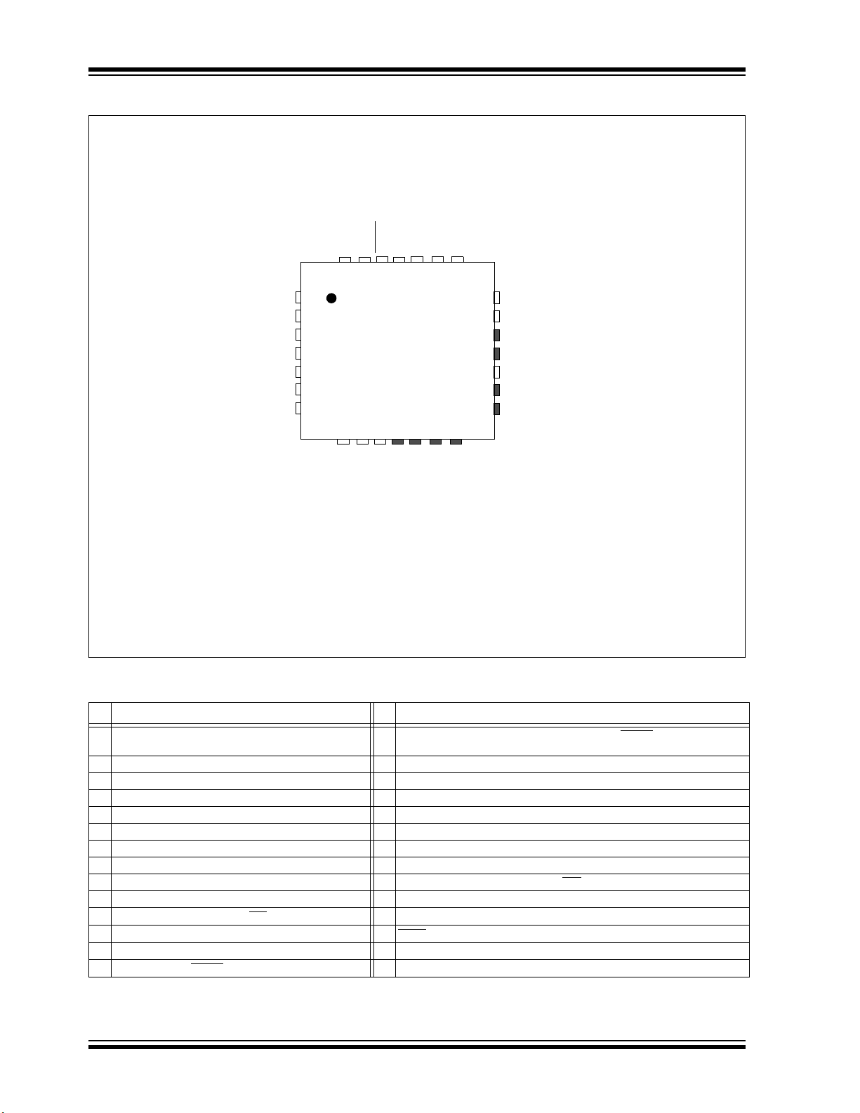
Pin Diagrams
28-Pin SSOP
1
2
3
4
5
6
7
8
9
10
11
12
13
14
28
27
26
25
24
23
22
21
20
19
18
17
16
15
MCLR
PGEC2/RP1/RA0
PGED2/RP2/RA1
PGED1/RP6/RB0
PGEC1/RP7/RB1
RP8/RB2
TDI/RP9/RB3
V
SS
OSC1/RP3/RA2
OSC2/RP4/RA3
(1)
SOSCI/RP10/RB4
SOSCO/RP5/RA4
V
DD
PGED3/RP11/RB5
V
BUS/RB6
RP12/RB7
TCK/RP13/RB8
(1)
TMS/RP14/RB9
(1,2)
PGEC3/TDO/RP18/RC9
(1)
VCAP
D-/RB10
D+/RB11
V
USB3V3
RP15/RB13
(1)
RP16/RB14
RP17/RB15
(1)
AVSS/VSS
AVDD/VDD
Legend: Shaded pins are up to 5V tolerant.
Note 1: High drive strength pin.
2: This pin may toggle during ICSP programming. Refer to Section 2.6 “JTAG”.
PIC32MM0256GPM028
PIC32MM0256GPM064 FAMILY
TABLE 2: COMPLETE PIN FUNCTION DESCRIPTIONS FOR 28-PIN SSOP DEVICES
Pin Function Pin Function
1MCLR 15 VBUS/RB6
2PGEC2/V
3PGED2/V
4 PGED1/AN2/C1IND/C2INB/C3INC/RP6/OCM2C/RB0 18 TMS/REFCLKI/RP14/SDA1/T1CK/T1G/T2CK/T2G/U1RTS/U1BCLK/SDO1/OCM1B/
5 PGEC1/AN3/C1INC/C2INA/RP7/OCM2D/RB1 19 PGEC3/TDO/RP18/ASCL1
6 AN4/C1INB/RP8/SDA2/OCM2E/RB2 20 VCAP
7 TDI/AN11/C1INA/RP9/SCL2/OCM2F/RB3 21 D-/RB10
8V
SS 22 D+/RB11
9 OSC1/CLKI/AN5/RP3/OCM1C/RA2 23 V
10 OSC2/CLKO/AN6/C3IND/RP4/OCM1D/RA3
11 SOSCI/AN7/RP10/OCM3C/RB4 25 CVREF/AN9/C3INB/RP16/RTCC/U1TX/VBUSON/SDI1/OCM3B/INT1/RB14
12 SOSCO/SCLKI/RP5/PWRLCLK/OCM3D/RA4 26 AN10/C3INA/REFCLKO/RP17/U1RX/SS1
13 VDD 27 AVSS/VSS
14 PGED3/RP11/ASDA1
OCM3E/RB5
Note 1: High drive strength pin.
2: Alternate pin assignments for I2C1 as determined by the I2C1SEL Configuration bit.
3: This pin may toggle during ICSP programming. Refer to Section 2.6 “JTAG”.
REF+/CVREF+/AN0/RP1/OCM1E/INT3/RA0 16 RP12/SDA3/SDI3/OCM3F/RB7
REF-/AN1/RP2/OCM1F/RA1 17 TCK/RP13/SCL1/U1CTS/SCK1/OCM1A/RB8
(1)
(2)
/USBID/SS3/FSYNC3/
INT2/RB9
USB3V3
(1,3)
24 AN8/LVDIN/RP15/SCL3/SCK3/OCM3A/RB13
28 AVDD/VDD
(2)
/T3CK/T3G/USBOEN/SDO3/OCM2A/RC9
(1)
(1)
/FSYNC1/OCM2B/INT0/RB15
(1)
(1)
2016-2019 Microchip Technology Inc. DS60001387D-page 3
Page 4
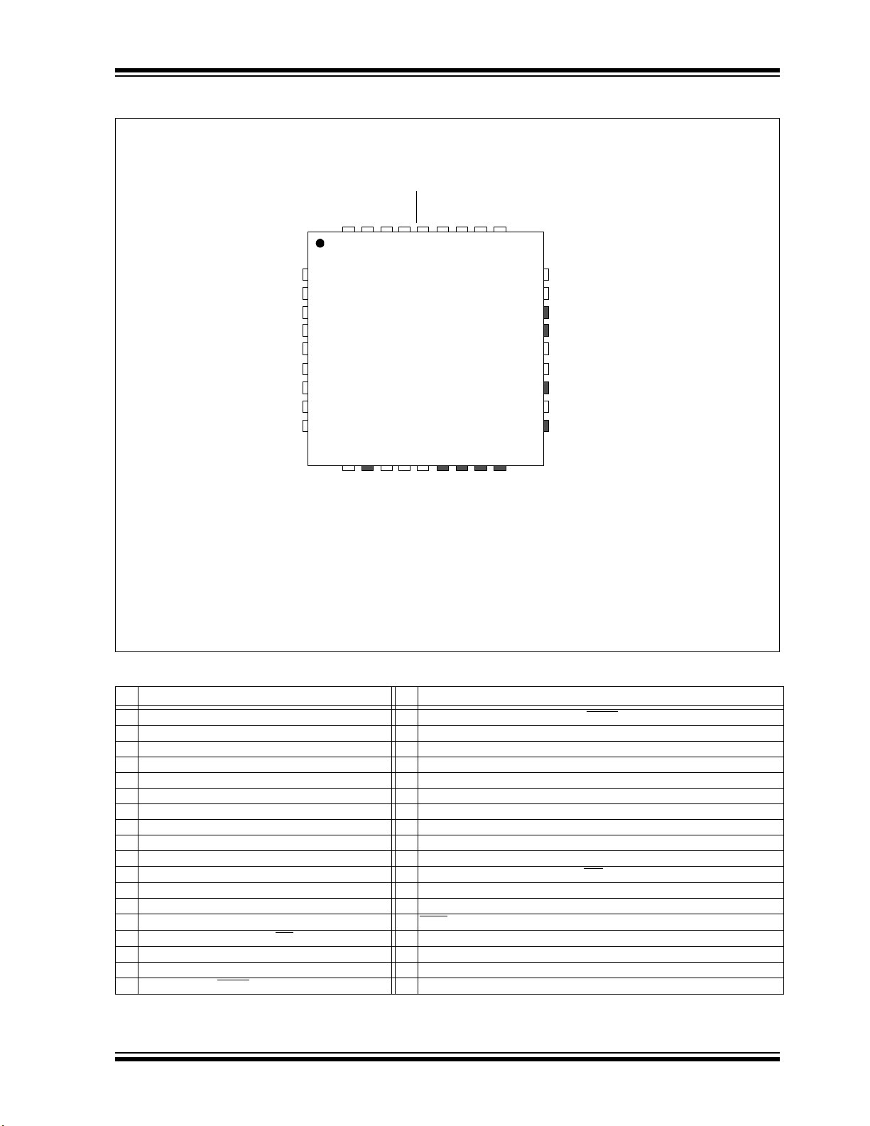
PIC32MM0256GPM064 FAMILY
28-Pin QFN/UQFN
(3)
10 11
2
3
6
1
18
19
20
21
22
12 13 14
15
8
7
16
17
232425262728
9
5
4
PGEC1/RP7/RB1
RP8/RB2
TDI/RP9/RB3
Vss
OSC1/RP3/RA2
OSC2/RP4/RA3
(1)
PGED1/RP6/RB0
SOSCI/RP10/RB4
SOSCO/RP5/RA4
V
DD
PGED3/RP11/RB5
V
BUS/RB6
RP12/RB7
TCK/RP13/RB8
(1)
TMS/RP14/RB9
(1,2)
PGEC3/TDO/RP18/RC9
(1)
VCAP
D-/RB10
D+/RB11
V
USB3V3
RP15/RB13
(1)
RP16/RB14
RP17/RB15
(1)
AVSS/VSS
AVDD/VDD
MCLR
PGEC2/RP1/RA0
PGED2/RP2/RA1
PIC32MM0256GPM028
Legend: Shaded pins are up to 5V tolerant.
Note 1: High drive strength pin.
2: This pin may toggle during ICSP programming. Refer to Section 2.6 “JTAG”.
3: The back side thermal pad is not electrically connected.
Pin Diagrams (Continued)
TABLE 3: COMPLETE PIN FUNCTION DESCRIPTIONS FOR 28-PIN QFN/UQFN DEVICES
Pin Function Pin Function
1 PGED1/AN2/C1IND/C2INB/C3INC/RP6/OCM2C/RB0 15 TMS/REFCLKI/RP14/SDA1/T1CK/T1G/T2CK/T2G/U1RTS/U1BCLK/SDO1/
2 PGEC1/AN3/C1INC/C2INA/RP7/OCM2D/RB1 16 PGEC3/TDO/RP18/ASCL1
3 AN4/C1INB/RP8/SDA2/OCM2E/RB2 17 VCAP
4 TDI/AN11/C1INA/RP9/SCL2/OCM2F/RB3 18 D-/RB10
5V
SS 19 D+/RB11
6 OSC1/CLKI/AN5/RP3/OCM1C/RA2 20 V
7 OSC2/CLKO/AN6/C3IND/RP4/OCM1D/RA3
8 SOSCI/AN7/RP10/OCM3C/RB4 22 CVREF/AN9/C3INB/RP16/RTCC/U1TX/VBUSON/SDI1/OCM3B/INT1/RB14
9 SOSCO/SCLKI/RP5/PWRLCLK/OCM3D/RA4 23 AN10/C3INA/REFCLKO/RP17/U1RX/SS1
10 VDD 24 AVSS/VSS
11 PGED3 /RP11/ASDA1
12 VBUS/RB6 26 MCLR
13 RP12/SDA3/SDI3/OCM3F/RB7 27 PGEC2/VREF+/CVREF+/AN0/RP1/OCM1E/INT3/RA0
14 TCK/RP13/SCL1/U1CTS
Note 1: High drive strength pin.
2: Alternate pin assignments for I2C1 as determined by the I2C1SEL Configuration bit.
3: This pin may toggle during ICSP programming. Refer to Section 2.6 “JTAG”.
(2)
/USBID/SS3/FSYNC3/OCM3E/RB5 25 AVDD/VDD
/SCK1/OCM1A/RB8
(1)
(1)
21 AN8/LVDIN/RP15/SCL3/SCK3/OCM3A/RB13
28 PGED2/VREF-/AN1/RP2/OCM1F/RA1
OCM1B/INT2/RB9
USB3V3
(1,3)
(2)
/T3CK/T3G/USBOEN/SDO3/OCM2A/RC9
(1)
/FSYNC1/OCM2B/INT0/RB15
(1)
(1)
DS60001387D-page 4 2016-2019 Microchip Technology Inc.
Page 5
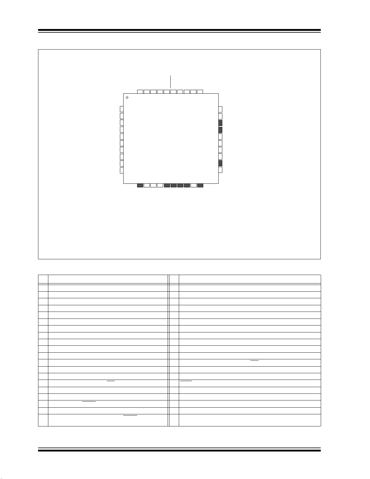
Pin Diagrams (Continued)
36-Pin QFN
(3)
RP8/RB2
TDI/RP9/RB3
RC0
RC1
RP19/RC2
V
SS
OSC1/RP3/RA2
OSC2/RP4/RA3
(1)
SOSCI/RP10/RB4
SOSCO/
RP5
/RA4
RP24/RA9
V
SS
VDD
RC3
V
BUS/RB6
RP12/RB7
TCK/
RP13
/RB8
(1)
TMS/RP14/RB9
(1,2)
RC8
PGEC3/TDO/RP18/RC9
(1)
VCAP
VDD
D+/RB11
V
USB3V3
D-/RB10
RP15/RB13
(1)
RP16/RB14
RP17/RB15
(1)
AVSS/VSS
AVDD/VDD
MCLR
PGEC2/
RP1
/RA0
PGED2/
RP2
/RA1
PGED1/
RP6
/RB0
PGEC1/
RP7
/RB1
9
1
2
3
4
5
161718
101112
13
31
7
6
3635343332
14
15
24
25
26
27
19
20
21
22
23
29
28
8
30
PIC32MM0256GPM036
PGED3/
RP11
/RB5
Legend: Shaded pins are up to 5V tolerant.
Note 1: High drive strength pin.
2: This pin may toggle during ICSP programming. Refer to Section 2.6 “JTAG”.
3: The back side thermal pad is not electrically connected.
PIC32MM0256GPM064 FAMILY
TABLE 4: COMPLETE PIN FUNCTION DESCRIPTIONS FOR 36-PIN QFN DEVICES
Pin Function Pin Function
1 AN4/C1INB/
2 TDI/AN11/C1INA/
3 AN12/C2IND/T2CK/T2G/RC0 21 PGEC3/TDO/
4 AN13/T3CK/T3G/RC1 22 V
5
RP19
6V
SS
7 OSC1/CLKI/AN5/
8 OSC2/CLKO/AN6/C3IND/
9 SOSCI/AN7/
10 SOSCO/SCLKI/
RP24
11
12 V
SS
13 V
DD
14 RC3 32 MCLR
15 PGED3/
BUS
16 V
RP12
17
18 TCK/
Note 1:
2:
3: This pin may toggle during ICSP programming. Refer to Section 2.6 “JTAG”.
RP8
/OCM2A/RC2 23 V
/OCM3A/RA9 29 AN10/C3INA/REFCLKO/
RP11
/RB6 34 PGED2/V
/SDA3/SDI3/OCM3F/RB7 35 PGED1/AN2/C1IND/C2INB/C3INC/
RP13
/SCL1/U1CTS/SCK1/OCM1A/RB8
High drive strength pin.
Alternate pin assignments for I2C1 as determined by the I2C1SEL Configuration bit.
/SDA2/OCM2E/RB2 19 TMS/REFCLKI/
RP9
/SCL2/OCM2F/RB3 20 AN14/LVDIN/C2INC/RC8
RP3
/OCM1C/RA2 25 D+/RB11
RP10
RP4
/OCM1D/RA3
/OCM3C/RB4 27 AN8/
RP5
/PWRLCLK/OCM3D/RA4 28 CV
(2)
/ASDA1
/USBID/SS3/FSYNC3/OCM3E/RB5 33 PGEC2/V
(1)
(1)
RP14
/SDA1/T1CK/T1G/U1RTS/U1BCLK/SDO1/OCM1B/INT2/RB9
CAP
DD
24 D-/RB10
26 V
USB3V3
RP15
REF
/AN9/C3INB/
30 AVSS/V
31 AVDD/V
36 PGEC1/AN3/C1INC/C2INA/
SS
DD
RP18
/ASCL1
/SCL3/SCK3/RB13
RP16
/RTCC/U1TX/VBUSON/SDI1/OCM3B/INT1/RB14
RP17
REF
+/CV
REF
+/AN0/
REF
-/AN1/
RP2
/OCM1F/RA1
(2)
/USBOEN/SDO3/RC9
(1)
/U1RX/SS1/FSYNC1/OCM2B/INT0/RB15
RP1
/OCM1E/INT3/RA0
RP6
/OCM2C/RB0
RP7
/OCM2D/RB1
(1,3)
(1)
(1)
2016-2019 Microchip Technology Inc. DS60001387D-page 5
Page 6
PIC32MM0256GPM064 FAMILY
40-Pin UQFN
(3)
111213141516171819
20
403938373635343332
31
29
28
27
26
25
24
23
22
30
10
RC0
RP8
/RB2
TDI/
RP9
/RB3
RC1
RP19
/RC2
V
SS
OSC1/
RP3
/RA2
OSC2/
RP4
/RA3
(1)
SOSCI/
RP10
/RB4
RP24
/RA9
V
SS
V
DD
RC3
PGED3/
RP11
/RB5
V
BUS
/RB6
RP12
/RB7
TCK/
RP13
/RB8
(1)
N/C
TMS/
RP14
/RB9
(1,2)
RC8
PGEC3/TDO/
RP18
/RC9
(1)
N/C
V
CAP
N/C
AV
DD
/V
DD
MCLR
PGEC2/
RP1
/RA0
PGED2/
RP2
/RA1
PGED1/
RP6
/RB0
PGEC1/
RP7
/RB1
N/C
AV
SS
/V
SS
RP17
/RB15
(1)
RP16
/RB14
111213141516171819
20
403938373635343332
31
29
28
27
26
25
24
23
22
21
30
10
V
DD
D-/RB10
D+/RB11
V
USB3V3
RP15
/RB13
(1)
1
2
3
4
5
6
7
8
9
PIC32MM0256GPM036
1
2
3
4
5
6
7
8
9
SOSCO/
RP5
/RA4
Legend: Shaded pins are up to 5V tolerant.
Note 1: High drive strength pin.
2: This pin may toggle during ICSP programming. Refer to Section 2.6 “JTAG”.
3: The back side thermal pad is not electrically connected.
Pin Diagrams (Continued)
TABLE 5: COMPLETE PIN FUNCTION DESCRIPTIONS FOR 40-PIN UQFN DEVICES
Pin Function Pin Function
1 AN4/C1INB/RP8/SDA2/OCM2E/RB2 21 AN14/LVDIN/C2INC/RC8
2 TDI/AN11/C1INA/RP9/SCL2/OCM2F/RB3 22 PGEC3/TDO/RP18/ASCL1
3 AN12/C2IND/T2CK/T2G/RC0 23 N/C
4 AN13/T3CK/T3G/RC1 24 V
5 RP19/OCM2A/RC2 25 N/C
6V
7 OSC1/CLKI/AN5/RP3/OCM1C/RA2 27 D-/RB10
8 OSC2/CLKO/AN6/C3IND/RP4/OCM1D/RA3
9 SOSCI/AN7/RP10/OCM3C/RB4 29 V
10 SOSCO/SCLKI/RP5/PWRLCLK/OCM3D/RA4 30 AN8/RP15/SCL3/SCK3/RB13
11 RP24/OCM3A/RA9 31 CVREF/AN9/C3INB/RP16/RTCC/U1TX/VBUSON/SDI1/OCM3B/INT1/RB14
12 V
13 VDD 33 AVSS/VSS
14 RC3 34 AVDD/VDD
15 PGED3/RP11/ASDA1
16 VBUS/RB6 36 PGEC2/VREF+/CVREF+/AN0/RP1/OCM1E/INT3/RA0
17 RP12/SDA3/SDI3/OCM3F/RB7 37 PGED2/V
18 TCK/RP13/SCL1/U1CTS
19 N/C 39 PGEC1/AN3/C1INC/C2INA/RP7/OCM2D/RB1
20 TMS/REFCLKI/RP14/SDA1/T1CK/T1G/U1RTS
Note 1:
SS 26 VDD
(2)
/USBID/SS3/FSYNC3/OCM3E/RB5 35 MCLR
SS 32 AN10/C3INA/REFCLKO/RP17/U1RX/SS1/FSYNC1/OCM2B/INT0/RB15
SDO1/OCM1B/INT2/RB9
High drive strength pin.
2:
Alternate pin assignments for I2C1 as determined by the I2C1SEL Configuration bit.
3: This pin may toggle during ICSP programming. Refer to Section 2.6 “JTAG”.
/SCK1/OCM1A/RB8
(1,3)
DS60001387D-page 6 2016-2019 Microchip Technology Inc.
(1)
(1)
/U1BCLK/
(2)
/SDO3/USBOEN/RC9
CAP
28 D+/RB11
USB3V3
38 PGED1/AN2/C1IND/C2INB/C3INC/RP6/OCM2C/RB0
40 N/C
(1)
REF-/AN1/RP2/OCM1F/RA1
(1)
(1)
Page 7

Pin Diagrams (Continued)
48-Pin UQFN, TQFP
(3)
10
11
2
3
4
5
6
1
1819202122
23
131415
38
8
7
4443424140
39
16
17
29
30
31
32
33
34
35
25
26
27
28
474546
9
37
12
24
36
48
PIC32MM0256GPM048
TMS/RP14/RB9
(1,2)
RP23/RC6
RP20/RC7
RC8
PGEC3/TDO/RP18/RC9
(1)
VSS
VCAP
RA15
D-/RB10
D+/RB11
V
USB3V3
RP15/RB13
(1)
RP22/RA10
(1)
RP21/RA7
RP16/RB14
RP17/RB15
(1)
AVSS/VSS
AVDD/VDD
MCLR
RA6
PGEC2/RP1/RA0
PGED2/RP2/RA1
PGED1/RP6/RB0
PGEC1/RP7/RB1
RP8/RB2
TDI/RP9/RB3
RC0
RC1
RP19/RC2
VDD
VSS
OSC1/RP3/RA2
OSC2/RP4/RA3
(1)
SOSCO/RP5/RA4
SOSCI/RP10/RB4
RA8
(1)
RP24/RA9
RD0
(1)
RC3
RC4
RC5
VSSVDD
RC12
RP12/RB7
PGED3/RP11/RB5
V
BUS/RB6
TCK/RP13/RB8
(1)
Legend: Shaded pins are up to 5V tolerant.
Note 1: High drive strength pin.
2: This pin may toggle during ICSP programming. Refer to Section 2.6 “JTAG”.
3: The back side thermal pad is not electrically connected.
PIC32MM0256GPM064 FAMILY
2016-2019 Microchip Technology Inc. DS60001387D-page 7
Page 8

PIC32MM0256GPM064 FAMILY
TABLE 6: COMPLETE PIN FUNCTION DESCRIPTIONS FOR 48-PIN UQFN/TQFP DEVICES
Pin Function Pin Function
1TMS/RP14/SDA1/OCM1B/INT2/RB9
(1,3)
2 RP23/RC6 26 TDI/AN11/C1INA/RP9/SCL2/OCM2F/RB3
3 RP20/RC7 27 AN12/C2IND/T2CK/T2G/RC0
4 AN14/LVDIN/C2INC/RC8 28 AN13/T3CK/T3G/RC1
5 PGEC3/TDO/RP18/ASCL1
6V
SS 30 VDD
(2)
/USBOEN/RC9
(1)
7VCAP 31 VSS
8 RTCC/RA15 32 OSC1/CLKI/AN5/RP3/OCM1C/RA2
9 D-/RB10 33 OSC2/CLKO/AN6/C3IND/RP4/RA3
10 D+/RB11 34 SDO3/RA8
11 VUSB3V3 35 SOSCI/AN7/RP10/OCM3C/RB4
12 AN8/RP15/SCL3/RB13
13 RP22/SCK3/RA10
(1)
(1)
14 RP21/SDI3/RA7 38 REFCLKI/T1CK/T1G/U1RTS
15 CVREF/AN9/C3INB/RP16/VBUSON/SDI1/OCM3B/INT1/RB14 39 OCM2B/RC3
16 AN10/C3INA/REFCLKO/RP17/SS1
17 AV
SS/VSS 41 AN15/OCM1D/RC5
18 AV
DD/VDD 42 VSS
/FSYNC1/INT0/RB15
(1)
19 MCLR 43 VDD
20 AN19/U1RX/RA6 44 U1TX/RC12
21 PGEC2/V
22 PGED2/V
REF+/CVREF+/AN0/RP1/RA0 45 PGED3/RP11/ASDA1
REF-/AN1/RP2/OCM1F/RA1 46 VBUS/RB6
23 PGED1/AN2/C1IND/C2INB/C3INC/RP6/OCM2C/RB0 47 RP12/SDA3/OCM3F/RB7
24 PGEC1/AN3/C1INC/C2INA/RP7/OCM2D/RB1 48 TCK/RP13/SCL1/U1CTS
Note 1: High drive strength pin.
2:
Alternate pin assignments for I2C1 as determined by the I2C1SEL Configuration bit.
3: This pin may toggle during ICSP programming. Refer to Section 2.6 “JTAG”.
25 AN4/C1INB/RP8/SDA2/OCM2E/RB2
29 RP19/OCM2A/RC2
(1)
(1)
36 SOSCO/SCLKI/RP5/PWRLCLK/OCM3D/RA4
37 RP24/OCM3A/RA9
/U1BCLK/SDO1/RD0
40 OCM1E/INT3/RC4
(2)
/USBID/SS3/FSYNC3/OCM3E/RB5
/SCK1/OCM1A/RB8
(1)
(1)
DS60001387D-page 8 2016-2019 Microchip Technology Inc.
Page 9

Pin Diagrams (Continued)
64-Pin QFN, TQFP
(3)
PIC32MM0256GPM064
646362616059585756555453525150
49
1
48
247
346
4
45
5
44
643
7
42
8
41
9
40
10 39
11
38
12 37
13
36
14
35
15 34
16 33
171819202122232425262728293031
32
RP22/RA10
(1)
RP15/RB13
(1)
VUSB3V3
D+/RB11
D-/RB10
RA14
RA15
VDDVCAP
PGEC3/TDO/RP18/RC9
(1)
RA5
RD1
RC8
RP20/RC7
RP23/RC6
TMS/RP14/RB9
(1,3)
TCK/RP13/RB8
(1)
RC13
(1)
RP12/RB7
RC10
V
BUS/RB6
PGED3/RP11/RB5
RC15
RC12
V
DD
VSS
RC5
RC4
RC3
RD0
(1)
RD3
VDD
VSS
RC0
RC1
RP19/RC2
RC11
V
DD
VSS
OSC1/RP3/RA2
OSC2/RP4/RA3
(1)
RA8
(1)
SOSCI/RP10/RB4
SOSCO/RP5/RA4
RP24/RA9
RD4
RD2
RP21/RA7
RP16/RB14
RP17/RB15
(1)
AVSS/VSS
AVDD/VDD
RA13
RA12
RA11
MCLR
RA6
PGEC2/RP1/RA0
PGED2/RP2/RA1
PGED1/RP6/RB0
PGEC1/RP7/RB1
RP8/RB2
TDI/RP9/RB3
RC14
Legend: Shaded pins are up to 5V tolerant.
Note 1: High drive strength pin.
2: This pin may toggle during ICSP programming. Refer to Section 2.6 “JTAG”.
3: The back side thermal pad is not electrically connected.
PIC32MM0256GPM064 FAMILY
2016-2019 Microchip Technology Inc. DS60001387D-page 9
Page 10

PIC32MM0256GPM064 FAMILY
TABLE 7: COMPLETE PIN FUNCTION DESCRIPTIONS FOR 64-PIN QFN/TQFP DEVICES
Pin Function Pin Function
1 RP21/SDI3/RA7 33 OCM3B/RD3
REF/AN9/C3INB/RP16/VBUSON/RB14 34 REFCLKI/T1CK/T1G/U1RTS/U1BCLK/SDO1/RD0
2CV
3 AN10/C3INA/REFCLKO/RP17/RB15
4AV
SS 36 OCM1E/INT3/RC4
5AV
DD 37 AN15/OCM1D/RC5
6 AN16/U1CTS
/RA13 38 VSS
(1)
35 OCM2B/RC3
7 AN17/OCM1A/RA12 39 VDD
8 AN18/RA11 40 U1TX/RC12
9MCLR
41 OCM3D/RC14
10 AN19/U1RX/RA6 42 OCM3E/RC15
11 PGEC2/V
12 PGED2/V
REF+/CVREF+/AN0/RP1/RA0 43 PGED3/RP11/ASDA1
REF-/AN1/RP2/OCM1F/RA1 44 VBUS/RB6
(2)
/USBID/RB5
13 PGED1/AN2/C1IND/C2INB/C3INC/RP6/OCM2C/RB0 45 OCM3F/RC10
14 PGEC1/AN3/C1INC/C2INA/RP7/OCM2D/RB1 46 RP12/SDA3/RB7
15 AN4/C1INB/RP8/SDA2/OCM2E/RB2 47 SCK1/RC13
16 TDI/AN11/C1INA/RP9/SCL2/OCM2F/RB3 48 TCK/RP13/SCL1/RB8
17 VDD 49 TMS/RP14/SDA1/INT2/RB9
(1)
(1)
(1,3)
18 VSS 50 RP23/RC6
19 AN12/C2IND/T2CK/T2G/RC0 51 RP20/RC7
20 AN13/T3CK/T3G/RC1 52 AN14/LVDIN/C2INC/RC8
21 RP19/OCM2A/RC2 53 OCM1B/RD1
22 SS3
/FSYNC3/RC11 54 OCM3A/RA5
23 V
DD 55 PGEC3/TDO/RP18/ASCL1
(2)
/USBOEN/RC9
24 VSS 56 VCAP
25 OSC1/CLKI/AN5/RP3/OCM1C/RA2 57 VDD
26 OSC2/CLKO/AN6/C3IND/RP4/RA3
27 SDO3/RA8
(1)
(1)
58 RTCC/RA15
59 OCM3C/RA14
28 SOSCI/AN7/RP10/RB4 60 D-/RB10
29 SOSCO/SCLKI/RP5/PWRLCLK/RA4 61 D+/RB11
30 RP24/RA9 62 V
31 SDI1/INT1/RD4 63 AN8/RP15/SCL3/RB13
32 SS1/FSYNC1/INT0/RD2 64 RP22/SCK3/RA10
USB3V3
(1)
(1)
Note 1: High drive strength pin.
2: Alternate pin assignments for I2C1 as determined by the I2C1SEL Configuration bit.
3: This pin may toggle during ICSP programming. Refer to Section 2.6 “JTAG”.
(1)
(1)
DS60001387D-page 10 2016-2019 Microchip Technology Inc.
Page 11

PIC32MM0256GPM064 FAMILY
Table of Contents
1.0 Device Overview ........................................................................................................................................................................ 15
2.0 Guidelines for Getting Started with 32-Bit Microcontrollers........................................................................................................ 23
3.0 CPU............................................................................................................................................................................................ 29
4.0 Memory Organization................................................................................................................................................................. 39
5.0 Flash Program Memory.............................................................................................................................................................. 45
6.0 Resets........................................................................................................................................................................................ 53
7.0 CPU Exceptions and Interrupt Controller ................................................................................................................................... 59
8.0 Direct Memory Access (DMA) Controller ................................................................................................................................... 77
9.0 Oscillator Configuration .............................................................................................................................................................. 97
10.0 I/O Ports ................................................................................................................................................................................... 113
11.0 Timer1 ...................................................................................................................................................................................... 127
12.0 Timer2 and Timer3 .................................................................................................................................................................. 131
13.0 Watchdog Timer (WDT) ........................................................................................................................................................... 137
14.0 Capture/Compare/PWM/Timer Modules (MCCP and SCCP) .................................................................................................. 141
15.0 Serial Peripheral Interface (SPI) and Inter-IC Sound (I2S)....................................................................................................... 157
16.0 Inter-Integrated Circuit (I2C) ..................................................................................................................................................... 165
17.0 Universal Asynchronous Receiver Transmitter (UART) ........................................................................................................... 173
18.0 USB On-The-Go (OTG)............................................................................................................................................................ 179
19.0 Real-Time Clock and Calendar (RTCC) ................................................................................................................................... 207
20.0 12-Bit ADC Converter with Threshold Detect........................................................................................................................... 215
21.0 Configurable Logic Cell (CLC).................................................................................................................................................. 227
22.0 Comparator .............................................................................................................................................................................. 243
23.0 Voltage Reference (CVREF) ..................................................................................................................................................... 249
24.0 High/Low-Voltage Detect (HLVD)............................................................................................................................................. 253
25.0 Power-Saving Features ........................................................................................................................................................... 257
26.0 Special Features ...................................................................................................................................................................... 263
27.0 Instruction Set .......................................................................................................................................................................... 281
28.0 Development Support............................................................................................................................................................... 283
29.0 Electrical Characteristics.......................................................................................................................................................... 285
30.0 Packaging Information.............................................................................................................................................................. 317
Appendix A: Revision History............................................................................................................................................................. 347
Index ................................................................................................................................................................................................. 349
The Microchip Website ...................................................................................................................................................................... 353
Customer Change Notification Service .............................................................................................................................................. 353
Customer Support .............................................................................................................................................................................. 353
Product Identification System ............................................................................................................................................................ 355
2016-2019 Microchip Technology Inc. DS60001387D-page 11
Page 12

PIC32MM0256GPM064 FAMILY
TO OUR VALUED CUSTOMERS
It is our intention to provide our valued customers with the best documentation possible to ensure successful use of your Microchip
products. To this end, we will continue to improve our publications to better suit your needs. Our publications will be refined and
enhanced as new volumes and updates are introduced.
If you have any questions or comments regarding this publication, please contact the Marketing Communications Department via
E-mail at docerrors@microchip.com. We welcome your feedback.
Most Current Data Sheet
To obtain the most up-to-date version of this data sheet, please register at our Worldwide Website at:
http://www.microchip.com
You can determine the version of a data sheet by examining its literature number found on the bottom outside corner of any page.
The last character of the literature number is the version number, (e.g., DS30000000A is version A of document DS30000000).
Errata
An errata sheet, describing minor operational differences from the data sheet and recommended workarounds, may exist for current
devices. As device/documentation issues become known to us, we will publish an errata sheet. The errata will specify the revision
of silicon and revision of document to which it applies.
To determine if an errata sheet exists for a particular device, please check with one of the following:
• Microchip’s Worldwide Website; http://www.microchip.com
• Your local Microchip sales office (see last page)
When contacting a sales office, please specify which device, revision of silicon and data sheet (include literature number) you are
using.
Customer Notification System
Register on our website at www.microchip.com to receive the most current information on all of our products.
DS60001387D-page 12 2016-2019 Microchip Technology Inc.
Page 13

PIC32MM0256GPM064 FAMILY
Referenced Sources
This device data sheet is based on the following
individual sections of the “PIC32 Family Reference
Manual”. These documents should be considered as
the general reference for the operation of a particular
module or device feature.
Note: To access the documents listed below,
browse the documentation section of the
Microchip website (www.microchip.com).
• Section 1. “Introduction” (www.microchip.com/DS60001127)
• Section 5. “Flash Programming” (www.microchip.com/DS60001121)
• Section 7. “Resets” (www.microchip.com/DS60001118)
• Section 8. “Interrupts” (www.microchip.com/DS60001108)
• Section 10. “Power-Saving Modes” (www.microchip.com/DS60001130)
• Section 12. “I/O Ports” (www.microchip.com/DS60001120)
• Section 14. “Timers” (www.microchip.com/DS60001105)
• Section 19. “Comparator” (www.microchip.com/DS60001110)
• Section 20. “Comparator Voltage Reference” (www.microchip.com/DS61109)
• Section 21. “UART” (www.microchip.com/DS60001107)
• Section 23. “Serial Peripheral Interface (SPI)” (www.microchip.com/DS61106)
• Section 24. “Inter-Integrated Circuit™ (I
• Section 25. “12-Bit Analog-to-Digital Converter (ADC) with Threshold Detect” (www.microchip.com/DS60001359)
• Section 27. “USB On-The-Go (OTG)” (www.microchip.com/DS61126)
• Section 28. “RTCC with Timestamp” (www.microchip.com/DS60001362)
• Section 30. “Capture/Compare/PWM/Timer (MCCP and SCCP)” (www.microchip.com/DS60001381)
• Section 31. “DMA Controller” (www.microchip.com/DS60001117)
• Section 33. “Programming and Diagnostics” (www.microchip.com/DS61129)
• Section 36. “Configurable Logic Cell” (www.microchip.com/DS60001363)
• Section 48. “Memory Organization and Permissions” (DS60001214)
• Section 50. “CPU for Devices with MIPS32
• Section 59. “Oscillators with DCO” (www.microchip.com/DS60001329)
• Section 62. “Dual Watchdog Timer” (www.microchip.com/DS60001365)
2
C™)” (www.microchip.com/DS60001116)
®
microAptiv™ and M-Class Cores” (www.microchip.com/DS60001192)
2016-2019 Microchip Technology Inc. DS60001387D-page 13
Page 14

PIC32MM0256GPM064 FAMILY
NOTES:
DS60001387D-page 14 2016-2019 Microchip Technology Inc.
Page 15

PIC32MM0256GPM064 FAMILY
UART1,2,3
Comparators
PORTA
PORTB
Priority
ISDS
EJTAGINT
Bus Matrix
RAM Peripheral Bridge
64
64-Bit Wide
Flash
32
32 32
Peripheral Bus Clocked by PBCLK
Program Flash Memory
Controller
32
32
32
Interrupt
Controller
PORTC
I2C1,2,3
SPI1,2,3
SCCP4-9
MCCP1,2,3
OSC1/CLKI
OSC2/CLKO
V
DD,
Timing
Generation
V
SS
MCLR
Power-up
Time r
Oscillator
Start-up Timer
Power-on
Reset
Watchdog
Time r
Brown-out
Reset
Precision
Reference
Band Gap
Regulator
Volt ag e
VCAP
Primary
Dividers
SYSCLK
PBCLK (1:1 with SYSCLK)
Peripheral Bus Clocked by PBCLK
PLL
RTCC
12-Bit ADC
Timer1,2,3
32
32
Oscillator
FRC/LPRC
Oscillators
SOSCO, SCLKI,
Secondary
Oscillator
AVDD, AVSS
I/O Change
Notification
HLVD
MIPS32® microAptiv™ UC
CPU Core
32
PORTD
DMA with
CRC
SOSCI
JTAG
BSCAN
32
Flash
Controller
32
USB
(write)
ICD
Flash Line
Buffer
1.0 DEVICE OVERVIEW
Note: This data sheet summarizes the features
of the PIC32MM0256GPM064 family of
devices. It is not intended to be a comprehensive reference source. To complement
the information in this data sheet, refer to
the PIC32 Family Reference Manuals,
This data sheet contains device-specific information for
the PIC32MM0256GPM064 family devices.
Figure 1-1 illustrates a general block diagram of the core
and peripheral modules in the PIC32MM0256GPM064
family of devices.
Table 1-1 lists the pinout I/O descriptions for the pins
shown in the device pin tables.
which are available from the Microchip
website (www.microchip.com/PIC32). The
information in this data sheet supersedes
the information in the FRM.
FIGURE 1-1: PIC32MM0256GPM064 FAMILY BLOCK DIAGRAM
2016-2019 Microchip Technology Inc. DS60001387D-page 15
Page 16

PIC32MM0256GPM064 FAMILY
TABLE 1-1: PIC32MM0256GPM064 FAMILY PINOUT DESCRIPTION
Pin Number
Pin
Pin Name
AN0 2 27 33 36 21 11 I ANA Analog-to-Digital Converter input channels
AN1 3 28 34 37 22 12 I ANA
AN2 4 1 35 382313IANA
AN3 5 2 36 392414IANA
AN4 6 3 1 1 25 15 I ANA
AN5 9 6 7 7 32 25 I ANA
AN6 10 7 8 8 33 26 I ANA
AN7 11 8 9 9 35 28 I ANA
AN8 24 21 27301263IANA
AN9 25 22 28 31 15 2 I ANA
AN10 26 23 29 32 16 3 I ANA
AN11 7 4 2 2 26 16 I ANA
AN12 — — 3 3 27 19 I ANA
AN13 — — 4 4 28 20 I ANA
AN14 — — 20 21 4 52 I ANA
AN15 — — — — 41 37 I ANA
AN16 — — — — — 6 I ANA
AN17 — — — — — 7 I ANA
AN18 — — — — — 8 I ANA
AN19 — — — — 20 10 I ANA
DD 28 25 31 34 18 5 P — Analog modules power supply
AV
AV
SS 27 24 30 33 17 4 P — Analog modules ground
C1INA 7 4 2 2 26 16 I ANA Comparator 1 Input A
C1INB 6 3 1 1 25 15 I ANA Comparator 1 Input B
C1INC 5 2 36 39 24 14 I ANA Comparator 1 Input C
C1IND 4 1 35 38 23 13 I ANA Comparator 1 Input D
C2INA 5 2 36 39 24 14 I ANA Comparator 2 Input A
C2INB 4 1 35 38 23 13 I ANA Comparator 2 Input B
C2INC — — 20 21 4 52 I ANA Comparator 2 Input C
C2IND — — 3 3 27 19 I ANA Comparator 2 Input D
C3INA 26 23 29 32 16 3 I ANA Comparator 3 Input A
C3INB 25 22 28 31 15 2 I ANA Comparator 3 Input B
C3INC 4 1 35 38 23 13 I ANA Comparator 3 Input C
C3IND 10 7 8 8 33 26 I ANA Comparator 3 Input D
CLKI 9 6 7 7 32 25 I ST External Clock source input (EC mode)
CLKO 10 7 8 8 33 26 O DIG System clock output
REF 25 22 28 31 15 2 O ANA Comparator voltage reference output
CV
REF+ 2 27 33 36 21 11 I ANA Positive comparator voltage reference input
CV
D+ 22 19 25 28 10 61 I/O — USB transceiver differential plus line
D- 21 18 24 27 9 60 I/O — USB transceiver differential minus line
FSYNC1 26 23 29 32 16 32 I/O ST/DIG SPI1 frame signal input or output
FSYNC3 14 11 15 15 45 22 I/O ST/DIG SPI3 frame signal input or output
Legend: ST = Schmitt Trigger input buffer DIG = Digital input/output P = Power
28-Pin
SSOP
I2C = I
28-Pin
QFN/
UQFN
2
C/SMBus input buffer ANA = Analog level input/output
36-Pin
QFN
40-Pin
UQFN
48-Pin
QFN/
TQFP
64-Pin
QFN/
TQFP
Typ e
Buffer
Typ e
Description
DS60001387D-page 16 2016-2019 Microchip Technology Inc.
Page 17

PIC32MM0256GPM064 FAMILY
TABLE 1-1: PIC32MM0256GPM064 FAMILY PINOUT DESCRIPTION (CONTINUED)
Pin Number
Pin
Pin Name
INT0 26 23 29 32 16 32 I ST External Interrupt 0
INT1 25 22 28 31 15 31 I ST External Interrupt 1
INT2 18 15 19 20 1 49 I ST External Interrupt 2
INT3 2 27 33 36 40 36 I ST External Interrupt 3
LVDIN 24 21 20 21 4 52 I ANA High/Low-Voltage Detect input
MCLR
OCM1A 17 14 18 18 48 7 O DIG MCCP1 Output A
OCM1B 18 15 19 20 1 53 O DIG MCCP1 Output B
OCM1C 9 6 7 7 32 25 O DIG MCCP1 Output C
OCM1D 10 7 8 8 41 37 O DIG MCCP1 Output D
OCM1E 2 27 33 36 40 36 O DIG MCCP1 Output E
OCM1F 3 28 34 37 22 12 O DIG MCCP1 Output F
OCM2A 19 16 5 5 29 21 O DIG MCCP2 Output A
OCM2B 26 23 29 32 39 35 O DIG MCCP2 Output B
OCM2C 4 1 35 38 23 13 O DIG MCCP2 Output C
OCM2D 5 2 36 39 24 14 O DIG MCCP2 Output D
OCM2E 6 3 1 1 25 15 O DIG MCCP2 Output E
OCM2F 7 4 2 2 26 16 O DIG MCCP2 Output F
OCM3A 24 21 11 11 37 54 O DIG MCCP3 Output A
OCM3B 25 22 28 31 15 33 O DIG MCCP3 Output B
OCM3C 11 8 9 9 35 59 O DIG MCCP3 Output C
OCM3D 12 9 10 10 36 41 O DIG MCCP3 Output D
OCM3E 14 11 15 15 45 42 O DIG MCCP3 Output E
OCM3F 16 13 17 17 47 45 O DIG MCCP3 Output F
OSC1 9 6 7 7 32 25 — — Primary Oscillator crystal
OSC2 10 7 8 8 33 26 — — Primary Oscillator crystal
PGEC1 5 2 36 39 24 14 I ST ICSP™ Port 1 programming clock input
PGEC2 2 27 33 36 21 11 I ST ICSP Port 2 programming clock input
PGEC3 19 16 21 22 5 55 I ST ICSP Port 3 programming clock input
PGED1 4 1 35 38 23 13 I/O ST/DIG ICSP Port 1 programming data
PGED2 3 28 34 37 22 12 I/O ST/DIG ICSP Port 2 programming data
PGED3 14 11 15 15 45 43 I/O ST/DIG ICSP Port 3 programming data
PWRLCLK 12 9 10 10 36 29 I ST Real-Time Clock 50/60 Hz clock input
Legend: ST = Schmitt Trigger input buffer DIG = Digital input/output P = Power
28-Pin
SSOP
I2C = I
28-Pin
QFN/
UQFN
1 26 32 35 19 9 I ST Master Clear (device Reset)
2
C/SMBus input buffer ANA = Analog level input/output
36-Pin
QFN
40-Pin
UQFN
48-Pin
QFN/
TQFP
64-Pin
QFN/
TQFP
Typ e
Buffer
Typ e
Description
2016-2019 Microchip Technology Inc. DS60001387D-page 17
Page 18

PIC32MM0256GPM064 FAMILY
TABLE 1-1: PIC32MM0256GPM064 FAMILY PINOUT DESCRIPTION (CONTINUED)
Pin Number
Pin
Pin Name
RA0 2 27 33 36 21 11 I/O ST/DIG PORTA digital I/Os
RA1 3 28 34 37 22 12 I/O ST/DIG
RA2 9 6 7 7 32 25 I/O ST/DIG
RA3 10 7 8 8 33 26 I/O ST/DIG
RA4 12 9 10 10 36 29 I/O ST/DIG
RA5 — — — — — 54 I/O ST/DIG
RA6 — — — — 20 10 I/O ST/DIG
RA7 — — — — 14 1 I/O ST/DIG
RA8 — — — — 34 27 I/O ST/DIG
RA9 — — 11 11 37 30 I/O ST/DIG
RA10 — — — — 13 64 I/O ST/DIG
RA11 — — — — — 8 I/O ST/DIG
RA12 — — — — — 7 I/O ST/DIG
RA13 — — — — — 6 I/O ST/DIG
RA14 — — — — — 59 I/O ST/DIG
RA15 — — — — 8 58 I/O ST/DIG
RB0 4 1 35 38 23 13 I/O ST/DIG PORTB digital I/Os
RB1 5 2 36 392414I/OST/DIG
RB2 6 3 1 1 25 15 I/O ST/DIG
RB3 7 4 2 2 26 16 I/O ST/DIG
RB4 11 8 9 9 35 28 I/O ST/DIG
RB5 14 11 15154543I/OST/DIG
RB6 15 12 16164644I/OST/DIG
RB7 16 13 17174746I/OST/DIG
RB8 17 14 18184848I/OST/DIG
RB9 18 15 19 20 1 49 I/O ST/DIG
RB10 21 18 24 27 9 60 I/O ST/DIG
RB11 22 19 25 28 10 61 I/O ST/DIG
RB13 24 21 27 30 12 63 I/O ST/DIG
RB14 25 22 28 31 15 2 I/O ST/DIG
RB15 26 23 29 32 16 3 I/O ST/DIG
Legend: ST = Schmitt Trigger input buffer DIG = Digital input/output P = Power
28-Pin
SSOP
I2C = I
28-Pin
QFN/
UQFN
2
C/SMBus input buffer ANA = Analog level input/output
36-Pin
QFN
40-Pin
UQFN
48-Pin
QFN/
TQFP
64-Pin
QFN/
TQFP
Typ e
Buffer
Typ e
Description
DS60001387D-page 18 2016-2019 Microchip Technology Inc.
Page 19

PIC32MM0256GPM064 FAMILY
TABLE 1-1: PIC32MM0256GPM064 FAMILY PINOUT DESCRIPTION (CONTINUED)
Pin Number
Pin
Pin Name
RC0 — — 3 3 27 19 I/O ST/DIG PORTC digital I/Os
RC1 — — 4 4 28 20 I/O ST/DIG
RC2 — — 5 5 29 21 I/O ST/DIG
RC3 — — 14 143935I/OST/DIG
RC4 — — — — 40 36 I/O ST/DIG
RC5 — — — — 41 37 I/O ST/DIG
RC6 — — — — 2 50 I/O ST/DIG
RC7 — — — — 3 51 I/O ST/DIG
RC8 — — 20 21 4 52 I/O ST/DIG
RC9 19 16 21 22 5 55 I/O ST/DIG
RC10 — — — — — 45 I/O ST/DIG
RC11 — — — — — 22 I/O ST/DIG
RC12 — — — — 44 40 I/O ST/DIG
RC13 — — — — — 47 I/O ST/DIG
RC14 — — — — — 41 I/O ST/DIG
RC15 — — — — — 42 I/O ST/DIG
RD0 — — — — 38 34 I/O ST/DIG PORTD digital I/Os
RD1 — — — — — 53 I/O ST/DIG
RD2 — — — — — 32 I/O ST/DIG
RD3 — — — — — 33 I/O ST/DIG
RD4 — — — — — 31 I/O ST/DIG
REFCLKI 18 15 19 20 38 34 I ST External reference clock input
REFCLKO 26 23 29 32 16 3 O ST External reference clock output
RP1 2 27 33 36 21 11 I/O ST/DIG Remappable peripherals (input or output)
RP2 3 28 34 37 22 12 I/O ST/DIG
RP3 9 6 7 7 32 25 I/O ST/DIG
RP4 10 7 8 8 33 26 I/O ST/DIG
RP5 12 9 10 10 36 29 I/O ST/DIG
RP6 4 1 35 382313I/OST/DIG
RP7 5 2 36 392414I/OST/DIG
RP8 6 3 1 1 25 15 I/O ST/DIG
RP9 7 4 2 2 26 16 I/O ST/DIG
RP10 11 8 9 9 35 28 I/O ST/DIG
RP11 14 11 15 15 45 43 I/O ST/DIG
RP12 16 13 17 17 47 46 I/O ST/DIG
RP13 17 14 18 18 48 48 I/O ST/DIG
RP14 18 15 19 20 1 49 I/O ST/DIG
RP15 24 21 27 30 12 63 I/O ST/DIG
RP16 25 22 28 31 15 2 I/O ST/DIG
RP17 26 23 29 32 16 3 I/O ST/DIG
RP18 19 16 21 22 5 55 I/O ST/DIG
RP19 — — 5 5 29 21 I/O ST/DIG
RP20 — — — — 3 51 I/O ST/DIG
Legend: ST = Schmitt Trigger input buffer DIG = Digital input/output P = Power
28-Pin
SSOP
I2C = I
28-Pin
QFN/
UQFN
2
C/SMBus input buffer ANA = Analog level input/output
36-Pin
QFN
40-Pin
UQFN
48-Pin
QFN/
TQFP
64-Pin
QFN/
TQFP
Typ e
Buffer
Typ e
Description
2016-2019 Microchip Technology Inc. DS60001387D-page 19
Page 20

PIC32MM0256GPM064 FAMILY
TABLE 1-1: PIC32MM0256GPM064 FAMILY PINOUT DESCRIPTION (CONTINUED)
Pin Number
Pin
Pin Name
RP21 — — — — 14 1 I/O ST/DIG Remappable peripherals (input or output)
RP22 — — — — 13 64 I/O ST/DIG
RP23 — — — — 2 50 I/O ST/DIG
RP2 4 — — 11 11 37 30 I /O S T/DIG
RTCC 25 22 28 31 8 58 O DIG Real-Time Clock/Calendar alarm/seconds
SCK1 17 14 18 18 48 47 I/O ST/DIG SPI1 clock (input or output)
SCK3 24 21 27 30 13 64 I/O ST/DIG SPI3 clock (input or output)
SCL1 17 14 18 18 48 48 I/O I2C I2C1 synchronous serial clock input/output
ASCL1 19 16 21 22 5 55 I/O I2C Alternate I2C1 synchronous serial clock input/
SCL2 7 4 2 2 26 16 I/O I2C I2C2 synchronous serial clock input/output
SCL3 24 21 27 30 12 63 I/O I2C I2C3 synchronous serial clock input/output
SCLKI 12 9 10 10 36 29 I ST Secondary Oscillator digital clock input
SDA1 18 15 19 20 1 49 I/O I2C I2C1 data input/output
ASDA1 14 11 15 15 45 43 I/O I2C Alternate I2C1 data input/output
SDA2 6 3 1 1 25 15 I/O I2C I2C2 data input/output
SDA3 16 13 17 17 47 46 I/O I2C I2C3 data input/output
SDI1 25 22 28 31 15 31 I ST SPI1 data input
SDI3 16 13 17 17 14 1 I ST SPI3 data input
SDO1 18 15 19 20 38 34 O DIG SPI1 data output
SDO3 19 16 21 22 34 27 O DIG SPI3 data output
SOSCI 11 8 9 9 35 28 — — Secondary Oscillator crystal
SOSCO 12 9 10 10 36 29 — — Secondary Oscillator crystal
SS1
SS3
T1CK 18 15 19 20 38 34 I ST Timer1 external clock input
T2CK 18 15 3 3 27 19 I ST Timer2 external clock input
T3CK 19 16 4 4 28 20 I ST Timer3 external clock input
T1G 18 15 19 20 38 34 I ST Timer1 clock gate input
T2G 18 15 3 3 27 19 I ST Timer2 clock gate input
T3G 19 16 4 4 28 20 I ST Timer3 clock gate input
TCK 17 14 18 18 48 48 I ST JTAG clock input
TDI 7 4 2 2 26 16 I ST JTAG data input
TDO 19 16 21 22 5 55 O DIG JTAG data output
TMS 18 15 19 20 1 49 I ST JTAG mode select input
Legend: ST = Schmitt Trigger input buffer DIG = Digital input/output P = Power
28-Pin
SSOP
I2C = I
28-Pin
QFN/
UQFN
26 23 29 32 16 32 I ST SPI1 slave select input
14 11 15 15 45 22 I ST SPI3 slave select input
2
C/SMBus input buffer ANA = Analog level input/output
36-Pin
QFN
40-Pin
UQFN
48-Pin
QFN/
TQFP
64-Pin
QFN/
TQFP
Typ e
Buffer
Typ e
Description
output
output
DS60001387D-page 20 2016-2019 Microchip Technology Inc.
Page 21

PIC32MM0256GPM064 FAMILY
TABLE 1-1: PIC32MM0256GPM064 FAMILY PINOUT DESCRIPTION (CONTINUED)
Pin Number
Pin
Pin Name
U1BCLK 18 15 19 20 38 34 O DIG UART1 IrDA® 16x baud clock output
U1CTS
U1RTS
U1RX 26 23 29 32 20 10 I ST UART1 receive data input
U1TX 25 22 28 31 44 40 O DIG UART1 transmit data output
USBID 14 11 15 15 45 43 I ST USB OTG ID (OTG mode only)
USBOEN 19 16 21 22 5 55 O — USB transceiver output enable flag
VBUSON 25 22 28 31 15 2 O — USB host and On-The-Go (OTG) bus power
BUS 15 12 16 16 46 44 P — USB VBUS connection (5V nominal)
V
V
USB3V3 23 20 26 29 11 62 P — USB transceiver power input (3.3V nominal)
CAP 20 17 22 24 7 56 P — Core voltage regulator filter capacitor
V
DD 13,28 10,25 13,23,31 13,26,
V
V
REF- 3 28 34 37 22 12 I ANA Analog-to-Digital Converter negative
REF+ 2 27 33 36 21 11 I ANA Analog-to-Digital Converter positive
V
SS 8,27 5,24 6,12,30 6,12,33 6,17,31,
V
Legend: ST = Schmitt Trigger input buffer DIG = Digital input/output P = Power
28-Pin
SSOP
I2C = I
28-Pin
QFN/
UQFN
17 14 18 18 48 6 I ST UART1 Clear-to-Send
18 15 19 20 38 34 O DIG UART1 Ready-to-Send
2
C/SMBus input buffer ANA = Analog level input/output
36-Pin
QFN
40-Pin
UQFN
34
48-Pin
TQFP
18,30,4317,23,
QFN/
42
64-Pin
QFN/
TQFP
39,57
18,24,38P — Digital modules ground
Buffer
Typ e
Typ e
control output; only available in external USB
Transceiver mode
connection
P — Digital modules power supply
reference
reference
Description
2016-2019 Microchip Technology Inc. DS60001387D-page 21
Page 22

PIC32MM0256GPM064 FAMILY
NOTES:
DS60001387D-page 22 2016-2019 Microchip Technology Inc.
Page 23

PIC32MM0256GPM064 FAMILY
2.0 GUIDELINES FOR GETTING STARTED WITH 32-BIT MICROCONTROLLERS
Note: This data sheet summarizes the features
of the PIC32MM0256GPM064 family of
devices. It is not intended to be a comprehensive reference source. To complement
the information in this data sheet, refer to the
“PIC32 Family Reference Manual”, which is
available from the Microchip website
www.microchip.com/PIC32). The infor-
(
mation in this data sheet supersedes the
information in the FRM.
2.1 Basic Connection Requirements
Getting started with the PIC32MM0256GPM064 family
of 32-bit Microcontrollers (MCUs) requires attention to
a minimal set of device pin connections before pro
ceeding with development. The following is a list of pin
names, which must always be connected:
•All VDD and VSS pins
(see Section 2.2 “Decoupling Capacitors”)
•All AVDD and AVSS pins, even if the ADC module
is not used (see
Capacitors”)
• MCLR pin (see Section 2.3 “Master Clear
(MCLR) Pin”)
•VCAP pin (see Section 2.4 “Voltage Regulator
Pin (VCAP)”)
• PGECx/PGEDx pins, used for In-Circuit Serial
Programming™ (ICSP™) and debugging
purposes (see Section 2.5 “ICSP Pins”)
• OSC1 and OSC2 pins, when external oscillator
source is used (see
Oscillator Pins”)
•VUSB3V3 pin, this pin must be powered for USB
operation (see Section 18.4 “Powering the USB
Transceiver”)
The following pin(s) may be required as well:
VREF+/VREF- pins, used when external voltage
reference for the ADC module is implemented
Note: The AVDD and AVSS pins must be
Section 2.2 “Decoupling
Section 2.7 “External
.
connected, regardless of ADC use and
the ADC voltage reference source.
2.2 Decoupling Capacitors
The use of decoupling capacitors on power supply
pins, such as V
Figure 2-1.
See
Consider the following criteria when using decoupling
capacitors:
• Value and type of capacitor: A value of 0.1 µF
(100 nF), 10-20V is recommended. The capacitor
should be a low Equivalent Series Resistance
(low-ESR) capacitor and have resonance frequency
in the range of 20
recommended that ceramic capacitors be used.
• Placement on the printed circuit board: The
decoupling capacitors should be placed as close to
the pins as possible. It is recommended that the
capacitors be placed on the same side of the board
as the device. If space is constricted, the capacitor
-
can be placed on another layer on the PCB using a
via; however, ensure that the trace length from the
pin to the capacitor is within one-quarter inch
mm) in length.
(6
• Handling high-frequency noise: If the board is
experiencing high-frequency noise, upward of tens
of MHz, add a second ceramic-type capacitor in
parallel to the above described decoupling capaci
tor. The value of the second capacitor can be in the
range of 0.01
capacitor next to the primary decoupling capacitor.
In high-speed circuit designs, consider implementing a decade pair of capacitances, as close to the
power and ground pins as possible. For example,
0.1 µF in parallel with 0.001 µF.
• Maximizing performance: On the board layout
from the power supply circuit, run the power and
return traces to the decoupling capacitors first, and
then to the device pins. This ensures that the
decoupling capacitors are first in the power chain.
Equally important is to keep the trace length
between the capacitor and the power pins to a
minimum, thereby reducing PCB track inductance.
DD, VSS, AVDD and AVSS, is required.
MHz and higher. It is further
-
µF to 0.001 µF. Place this second
2016-2019 Microchip Technology Inc. DS60001387D-page 23
Page 24

PIC32MM0256GPM064 FAMILY
PIC32
VDD
VSS
VDD
VSS
VSS
VDD
AVDD
AVSS
VDD
VSS
0.1 µF
Ceramic
0.1 µF
Ceramic
0.1 µF
Ceramic
0.1 µF
Ceramic
C
R
V
DD
MCLR
0.1 µF
Ceramic
R1
CEFC
10 µF
VCAP/VCORE
Note 1: Refer to Section 18.4 “Powering the USB
Transceiver” for requirements of this pin.
V
USB3V3
USB
Power
(1)
Note 1: 470 R1 1 k will limit any current flowing into
MCLR
from the external capacitor, C, in the event of
MCLR
pin breakdown, due to Electrostatic Discharge
(ESD) or Electrical Overstress (EOS). Ensure that the
MCLR
pin VIH and VIL specifications are met without
interfering with the debugger/programmer tools.
2: The capacitor can be sized to prevent unintentional
Resets from brief glitches or to extend the device
Reset period during POR.
3: No pull-ups or bypass capacitors are allowed on active
debug/program PGECx/PGEDx pins.
R1
(1)
10k
V
DD
MCLR
PIC32
1 k
0.1 µF
(2)
PGECx
(3)
PGEDx
(3)
ICSP™
1
5
4
2
3
6
V
DD
VSS
NC
R
C
FIGURE 2-1: RECOMMENDED
MINIMUM CONNECTION
2.2.1 BULK CAPACITORS
The use of a bulk capacitor is recommended to improve
power supply stability. Typical values range from 4.7 µF
to 47 µF. This capacitor should be located as close to
the device as possible.
For example, as illustrated in Figure 2-2, it is
recommended that the capacitor, C, be isolated from
the
MCLR pin during programming and debugging
operations.
Place the components illustrated in Figure 2-2 within
one-quarter inch (6 mm) from the MCLR pin.
FIGURE 2-2: EXAMPLE OF MCLR PIN
CONNECTIONS
(1,2,3)
2.3 Master Clear (MCLR) Pin
The MCLR pin provides for two specific device
functions:
•Device Reset
• Device Programming and Debugging
Pulling The MCLR pin low generates a device Reset.
Figure 2-2 illustrates a typical MCLR circuit. During
device programming and debugging, the resistance
and capacitance that can be added to the pin must
be considered. Device programmers and debuggers
drive the
levels (V
not be adversely affected. Therefore, specific values
of R and C will need to be adjusted based on the
application and PCB requirements.
Note: When MCLR is used to wake the device
DS60001387D-page 24 2016-2019 Microchip Technology Inc.
MCLR pin. Consequently, specific voltage
IH and VIL) and fast signal transitions must
from Retention Sleep, a POR Reset will
occur.
Page 25
PIC32MM0256GPM064 FAMILY
10
1
0.1
0.01
0.001
0.01 0.1 1 10 100 1000 10,000
Frequency (MHz)
ESR ()
Note: Typical data measurement at +25°C, 0V DC bias.
2.4 Voltage Regulator Pin (VCAP)
A low-ESR (< 5Ω) capacitor is required on the VCAP pin
to stabilize the output voltage of the on-chip voltage
regulator. The V
CAP pin must not be connected to VDD
FIGURE 2-3: FREQUENCY vs. ESR
PERFORMANCE FOR
SUGGESTED V
CAP
and must use a capacitor of 10 µF connected to ground.
The type can be ceramic or tantalum. Suitable examples
of capacitors are shown in
Table 2-1. Capacitors with
equivalent specification can be used.
The placement of this capacitor should be close to VCAP.
It is recommended that the trace length not exceed
inch (6 mm). Refer to Section 29.0 “Electrical
0.25
Characteristics” for additional information.
Designers may use Figure 2-3 to evaluate ESR
equivalence of candidate devices.
.
TABLE 2-1: SUITABLE CAPACITOR EQUIVALENTS
Make Part #
TDK C3216X7R1C106K 10 µF ±10% 16V -55 to +125ºC
TDK C3216X5R1C106K 10 µF ±10% 16V -55 to +85ºC
Panasonic ECJ-3YX1C106K 10 µF ±10% 16V -55 to +125ºC
Panasonic ECJ-4YB1C106K 10 µF ±10% 16V -55 to +85ºC
Murata GRM319R61C106KE15D 10 µF ±10% 16V -55 to +85ºC
Nominal
Capacitance
Base Tolerance Rated Voltage Temp. Rang e
2016-2019 Microchip Technology Inc. DS60001387D-page 25
Page 26

PIC32MM0256GPM064 FAMILY
-80
-70
-60
-50
-40
-30
-20
-10
0
10
5 1011121314151617
DC Bias Voltage (VDC)
Capacitance Change (%)
01234 67 89
6.3V Capacitor
10V Capacitor
16V Capacitor
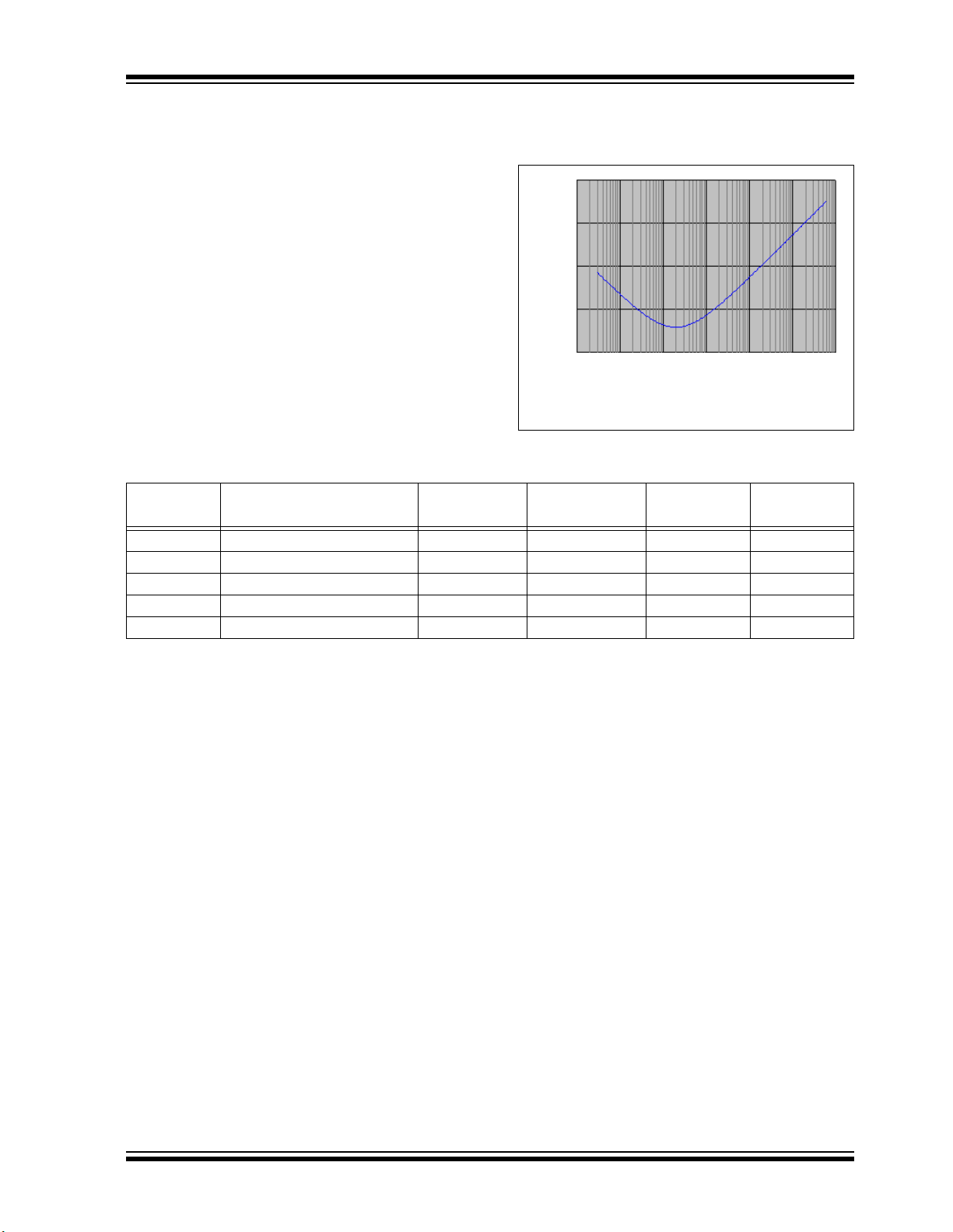
2.4.1 CONSIDERATIONS FOR CERAMIC CAPACITORS
In recent years, large value, low-voltage, surface-mount
ceramic capacitors have become very cost effective in
sizes up to a few tens of microfarad. The low-ESR, small
physical size and other properties make ceramic
capacitors very attractive in many types of applications.
Ceramic capacitors are suitable for use with the internal voltage regulator of this microcontroller. However,
some care is needed in selecting the capacitor to
ensure that it maintains sufficient capacitance over the
intended operating range of the application.
Typical low-cost, 10 µF ceramic capacitors are available
in X5R, X7R and Y5V dielectric ratings (other types are
also available, but are less common). The initial
tolerance specifications for these types of capacitors
are often specified as ±10% to ±20% (X5R and X7R)
or -20%/+80% (Y5V). However, the effective capaci
tance that these capacitors provide in an application
circuit will also vary based on additional factors, such as
the applied DC bias voltage and the temperature. The
total in-circuit tolerance is, therefore, much wider than
the initial tolerance specification.
The X5R and X7R capacitors typically exhibit satisfactory temperature stability (ex: ±15% over a wide
temperature range, but consult the manufacturer’s data
sheets for exact specifications). However, Y5V capacitors typically have extreme temperature tolerance
specifications of +22%/-82%. Due to the extreme
temperature tolerance, a 10 µF nominal rated Y5V type
capacitor may not deliver enough total capacitance to
meet minimum internal voltage regulator stability and
transient response requirements. Therefore, Y5V
capacitors are not recommended for use with the
internal regulator.
In addition to temperature tolerance, the effective
capacitance of large value ceramic capacitors can vary
substantially, based on the amount of DC voltage applied
to the capacitor. This effect can be very significant, but is
often overlooked or is not always documented.
Typical DC bias voltage vs. capacitance graph for X7R
type capacitors is shown in
Figure 2-4.
-
When selecting a ceramic capacitor to be used with the
internal voltage regulator, it is suggested to select a
high-voltage rating, so that the operating voltage is a
small percentage of the maximum rated capacitor
voltage. The minimum DC rating for the ceramic
capacitor on V
shown in
CAP is 16V. Suggested capacitors are
Table 2-1.
2.5 ICSP Pins
The PGECx and PGEDx pins are used for In-Circuit
Serial Programming™ (ICSP™) and debugging pur
poses. It is recommended to keep the trace length
between the ICSP connector and the ICSP pins on
the device as short as possible. If the ICSP connec
tor is expected to experience an ESD event, a series
resistor is recommended, with the value in the range
of a few tens of Ohms, not to exceed 100 Ohms.
Pull-up resistors, series diodes and capacitors on the
PGECx and PGEDx pins are not recommended as they
will interfere with the programmer/debugger communications to the device. If such discrete components are
an application requirement, they should be removed
from the circuit during programming and debugging.
Alternatively, refer to the AC/DC characteristics and
timing requirements information in the respective
device Flash programming specification for information
on capacitive loading limits and pin Input Voltage High
IH) and Input Voltage Low (VIL) requirements.
(V
Ensure that the “Communication Channel Select”
(i.e., PGECx/PGEDx pins) programmed into the device
matches the physical connections for the ICSP to
MPLAB
®
ICD 3 or MPLAB REAL ICE™ In-Circuit
Emulator.
For more information on MPLAB® ICD 3 and REAL ICE
connection requirements, refer to the following
documents that are available from the Microchip website.
• “Using MPLAB® ICD 3” (poster) (DS51765)
• “Development Tools Design Advisory” (DS51764)
• “MPLAB® REAL ICE™ In-Circuit Emulator User’s
Guide” (DS51616)
• “Using MPLAB® REAL ICE™ In-Circuit Emulator”
(poster) (DS51749)
-
-
FIGURE 2-4: DC BIAS VOLTAGE vs.
DS60001387D-page 26 2016-2019 Microchip Technology Inc.
CAPACITANCE
CHARACTERISTICS
Page 27

PIC32MM0256GPM064 FAMILY
Main Oscillator
Guard Ring
Guard Trace
Secondary
Oscillator
2.6 JTAG
The TMS, TDO, TDI and TCK pins are used for testing
and debugging according to the Joint Test Action Group
(JTAG) standard. It is recommended to keep the trace
length between the JTAG connector, and the JTAG pins
on the device, as short as possible. If the JTAG connector
is expected to experience an ESD event, a series resistor
is recommended, with the value in the range of a few tens
of Ohms, not to exceed 100
Pull-up resistors, series diodes and capacitors on the
TMS, TDO, TDI and TCK pins are not recommended as
they will interfere with the programmer/debugger communications to the device. If such discrete components
are an application requirement, they should be removed
from the circuit during programming and debugging.
Alternatively, refer to the AC/DC characteristics and
timing requirements information in the respective device
Flash programming specification for information on
capacitive loading limits, and pin Input Voltage High (V
and Input Voltage Low (V
Note 1: The TMS pin function may be active
multiple times during ICSP device Erase,
Programming and Debugging. When the
TMS function is active, the integrated
pull-up resistor, ~6k, will pull the pin to
DD. When the TMS function is inactive,
V
the pin will be tri-state. The TMS function
being enabled and disabled repeatedly
results in the pin “toggling.”
• Do not connect circuity to the TMS
pin that could be adversely affected
by the toggling.
• If circuity connected to the TMS pin
is sensitive to the “toggling” do not
program the device in circuit.
• Use a strong pull-down resistor
such as 1k between the TMS pin to
ground to overpower the pull-up.
Ohms.
IH)
IL) requirements.
2.7 External Oscillator Pins
This family of devices has options for two external
oscillators: a high-frequency Primary Oscillator and a
low-frequency Secondary Oscillator (refer to
Section 9.0 “Oscillator Configuration” for details).
The oscillator circuit should be placed on the same side
of the board as the device. Also, place the oscillator
circuit close to the respective oscillator pins, not
exceeding one-half inch (12 mm) distance between
them. The load capacitors should be placed next to the
oscillator itself, on the same side of the board. Use a
grounded copper pour around the oscillator circuit to
isolate them from surrounding circuits. The grounded
copper pour should be routed directly to the MCU
ground. Do not run any signal traces or power traces
inside the ground pour. Also, if using a two-sided board,
avoid any traces on the other side of the board where
the crystal is placed. A suggested layout is illustrated in
Figure 2-5.
For additional information and design guidance on
oscillator circuits, please refer to these Microchip
Application Notes, available at the corporate website:
(www.microchip.com).
•AN826, “Crystal Oscillator Basics and Crystal
Selection for rfPIC™ and PICmicro
•AN849, “Basic PICmicro® Oscillator Design”
•AN943, “Practical PICmicro® Oscillator Analysis
and Design”
•AN949, “Making Your Oscillator Work”
®
Devices”
FIGURE 2-5: SUGGESTED OSCILLATOR
CIRCUIT PLACEMENT
2.8 Unused I/Os
To minimize power consumption, unused I/O pins
should not be allowed to float as inputs. They can be
configured as outputs and driven to a logic low or logic
high state.
Alternatively, inputs can be reserved by ensuring the
pin is always configured as an input and externally con
necting the pin to VSS or VDD. A current-limiting resistor
may be used to create this connection if there is any
risk of inadvertently configuring the pin as an output
with the logic output state opposite of the chosen power
rail.
-
2016-2019 Microchip Technology Inc. DS60001387D-page 27
Page 28

PIC32MM0256GPM064 FAMILY
NOTES:
DS60001387D-page 28 2016-2019 Microchip Technology Inc.
Page 29

PIC32MM0256GPM064 FAMILY
3.0 CPU
Note: This data sheet summarizes the features
of the PIC32MM0256GPM064 family of
devices. It is not intended to be a
comprehensive reference source. To
complement the information in this data
sheet, refer to Section 50. “CPU for
Devices with MIPS32
M-Class Cores” (www.microchip.com/
DS60001192) in the “PIC32 Family Refer
ence Manual”. MIPS32® microAptiv™ UC
microprocessor core resources are available at: www.imgtec.com. The information
in this data sheet supersedes the
information in the FRM.
The MIPS32® microAptiv™ UC microprocessor core is
the heart of the PIC32MM0256GPM064 family
devices. The CPU fetches instructions, decodes each
instruction, fetches source operands, executes each
instruction and writes the results of the instruction
execution to the proper destinations.
3.1 Features
The PIC32MM0256GPM064 family processor core key
features include:
• Five-Stage Pipeline
• 32-Bit Address and Data Paths
• MIPS32 Enhanced Architecture:
- Multiply-add and multiply-subtract instructions.
- Targeted multiply instruction.
- Zero and one detect instructions.
- WAIT instruction.
- Conditional move instructions.
- Vectored interrupts.
- Atomic interrupt enable/disable.
- One GPR shadow set to minimize latency of
interrupts.
- Bit field manipulation instructions.
• microMIPS™ Instruction Set:
- microMIPS allows improving the code size
density over MIPS32, while maintaining
MIPS32 performance.
- microMIPS supports all MIPS32 instructions
(except for branch-likely instructions) with
new optimized 32-bit encoding. Frequent
MIPS32 instructions are available as 16-bit
instructions.
- Added seventeen new and thirty-five
MIPS32
instructions in 16-bit opcode format.
- Stack Pointer implicit in instruction.
- MIPS32 assembly and ABI compatible.
®
corresponding, commonly used
®
microAptiv™ and
-
• Memory Management Unit with Simple Fixed
Mapping Translation (FMT) Mechanism
• Multiply/Divide Unit (MDU):
- Configurable using high-performance
multiplier array.
- Maximum issue rate of one 32x16 multiply
per clock.
- Maximum issue rate of one 32x32 multiply
every other clock.
- Early-in iterative divide. Minimum 11 and
maximum 33 clock latency (dividend (rs) sign
extension dependent).
• Power Control:
- No minimum frequency: 0 MHz.
- Power-Down mode (triggered by WAIT
instruction).
• EJTAG Debug/Profiling:
- CPU control with start, stop and single
stepping.
- Software breakpoints via the SDBBP
instruction.
- Simple hardware breakpoints on virtual
addresses, four instructions and
two data breakpoints.
- PC and/or load/store address sampling for
profiling.
- Performance counters.
- Supports Fast Debug Channel (FDC).
A block diagram of the PIC32MM0256GPM064 family
processor core is shown in
Figure 3-1.
2016-2019 Microchip Technology Inc. DS60001387D-page 29
Page 30

PIC32MM0256GPM064 FAMILY
System Bus
Execution Unit
ALU/Shift
Atomic/LdSt
MCU ASE
System
Coprocessor
Enhanced MDU
GPR
(two sets)
Debug/Profiling
Breakpoints
Fast Debug Channel
Performance Counters
Power
System
Interface
Interrupt
Interface
MMU
Decode
(microMIPS™)
EJTAG
2-Wire Debug
Management
SYSCLK
MIPS32® microAptiv™ UC Microprocessor Core
FIGURE 3-1: PIC32MM0256GPM064 FAMILY MICROPROCESSOR CORE BLOCK DIAGRAM
DS60001387D-page 30 2016-2019 Microchip Technology Inc.
Page 31

PIC32MM0256GPM064 FAMILY
3.2 Architecture Overview
The MIPS32® microAptiv™ UC microprocessor core in
the PIC32MM0256GPM064 family devices contains
several logic blocks, working together in parallel, pro
viding an efficient high-performance computing engine.
The following blocks are included with the core:
• Execution Unit
• General Purpose Register (GPR)
• Multiply/Divide Unit (MDU)
• System Control Coprocessor (CP0)
• Memory Management Unit (MMU)
• Power Management
• microMIPS Instructions Decoder
• Enhanced JTAG (EJTAG) Controller
3.2.1 EXECUTION UNIT
The processor core execution unit implements a load/
store architecture with single-cycle ALU operations
(logical, shift, add, subtract) and an autonomous Multiply/
Divide Unit (MDU). The core contains thirty-two 32-bit
General Purpose Registers (GPRs) used for integer
operations and address calculation. One additional
register file shadow set (containing thirty-two registers) is
added to minimize context switching overhead during
interrupt/exception processing. The register file consists
of two read ports and one write port, and is fully bypassed
to minimize operation latency in the pipeline.
The execution unit includes:
• 32-bit adder used for calculating the data address
• Address unit for calculating the next instruction address
• Logic for branch determination and branch target
address calculation
• Load aligner
• Bypass multiplexers used to avoid Stalls when
executing instruction streams where data producing instructions are followed closely by consumers
for their results
• Leading zero/one detect unit for implementing the
CLZ and CLO instructions
• Arithmetic Logic Unit (ALU) for performing
arithmetic and bitwise logical operations
• Shifter and store aligner
-
3.2.2 MULTIPLY/DIVIDE UNIT (MDU)
The microAptiv UC core includes a Multiply/Divide Unit
(MDU) that contains a separate pipeline for multiply
and divide operations. This pipeline operates in parallel
with the Integer Unit (IU) pipeline and does not stall
when the IU pipeline stalls. This allows the longrunning MDU operations to be partially masked by
system Stalls and/or other Integer Unit instructions.
The high-performance MDU consists of a 32x16 booth
recoded multiplier, Result/Accumulation registers (HI
and LO), a divide state machine, and the necessary
multiplexers and control logic. The first number shown
(‘32’ of 32x16) represents the rs operand. The second
number (‘16’ of 32x16) represents the rt operand. The
microAptiv UC core only checks the value of the rt
operand to determine how many times the operation
must pass through the multiplier. The 16x16 and 32x16
operations pass through the multiplier once. A 32x32
operation passes through the multiplier twice.
The MDU supports execution of one 16x16 or 32x16
multiply operation every clock cycle; 32x32 multiply
operations can be issued every other clock cycle. Appropriate interlocks are implemented to stall the issuance of
back-to-back, 32x32 multiply operations. The multiply
operand size is automatically determined by logic built
into the MDU. Divide operations are implemented with a
simple 1-bit-per-clock iterative algorithm. An early-in
detection checks the sign extension of the dividend (rs)
operand. If rs is 8 bits wide, 23 iterations are skipped.
For a 16-bit wide rs, 15 iterations are skipped, and for a
24-bit wide rs, 7 iterations are skipped. Any attempt to
issue a subsequent MDU instruction while a divide is still
active causes an IU pipeline Stall until the divide
operation has completed.
Table 3-1 lists the repeat rate (peak issue rate of cycles
until the operation can be re-issued), and latency
(number of cycles until a result is available) for the
microAptiv UC core multiply and divide instructions.
The approximate latency and repeat rates are listed in
terms of pipeline clocks.
TABLE 3-1: MULTIPLY/DIVIDE UNIT LATENCIES AND REPEAT RATES
Opcode Operand Size (mul rt) (div rs) Latency Repeat Rate
MULT/MULTU, MADD/MADDU,
MSUB/MSUBU
MUL (GPR destination) 16 bits 2 1
DIV/DIVU 8 bits 12 11
2016-2019 Microchip Technology Inc. DS60001387D-page 31
16 bits 1 1
32 bits 2 2
32 bits 3 2
16 bits 19 18
24 bits 26 25
32 bits 33 32
Page 32

PIC32MM0256GPM064 FAMILY
The MIPS® architecture defines that the result of a
multiply or divide operation be placed in the HI and LO
registers. Using the Move-From-HI (MFHI) and MoveFrom-LO (MFLO) instructions, these values can be
transferred to the general purpose register file.
In addition to the HI/LO targeted operations, the MIPS
architecture also defines a Multiply instruction, MUL,
which places the least significant results in the primary
register file instead of the HI/LO register pair. By avoid
ing the explicit MFLO instruction, required when using the
LO register, and by supporting multiple destination
registers, the throughput of multiply-intensive operations
is increased.
Two other instructions, Multiply-Add (MADD) and
Multiply-Subtract (MSUB), are used to perform the
multiply-accumulate and multiply-subtract operations.
The MADD instruction multiplies two numbers and then
adds the product to the current contents of the HI and
LO registers. Similarly, the MSUB instruction multiplies
two operands and then subtracts the product from the
HI and LO registers. The MADD and MSUB operations
are commonly used in DSP algorithms.
-
3.2.3 SYSTEM CONTROL
COPROCESSOR (CP0)
In the MIPS architecture, CP0 is responsible for the
virtual-to-physical address translation, the exception
control system, the processor’s diagnostics capability,
the operating modes (Kernel, User and Debug) and
whether interrupts are enabled or disabled. These
configuration options and other system information are
available by accessing the CP0 registers listed in
Table 3-2.
DS60001387D-page 32 2016-2019 Microchip Technology Inc.
Page 33

PIC32MM0256GPM064 FAMILY
TABLE 3-2: COPROCESSOR 0 REGISTERS
Register
Number
0-3
4 UserLocal User information that can be written by privileged software and read via
5-6
7 HWREna Enables access via the RDHWR instruction to selected hardware registers in
8BadVAddr
9 Count
10 Reserved Reserved in the microAptiv UC.
11 Compare
12 Status/
13 Cause
14 EPC
15 PRId/
16 CONFIG/
7-22
23 Debug/
24 DEPC
25 PerfCtl0/
26 ErrCtl Software parity check enable.
27 CacheErr Records information about SRAM parity errors.
28-29
30 ErrorEPC
31 DeSAVE
Note 1: Registers used in exception processing.
2: Registers used in debug.
Register
Name
Reserved Reserved in the microAptiv™ UC.
RDHWR Register 29.
Reserved Reserved in the microAptiv UC.
Non-Privileged mode.
(1)
(1)
(1)
Reports the address for the most recent address related exception.
Processor cycle count.
Timer interrupt control.
Processor status and control; interrupt control and shadow set control.
IntCtl/
SRSCtl/
SRSMap1/
View_IPL/
SRSMAP2
(1)
/
Cause of last exception.
View_RIPL
(1)
Program Counter at last exception.
Processor identification and revision; exception base address; Common Device
EBase/
Memory Map Base register.
CDMMBase
Configuration registers.
CONFIG1/
CONFIG2/
CONFIG3/
CONFIG7
Reserved Reserved in the microAptiv UC.
EJTAG Debug register.
Debug2/
TraceControl/
TraceControl2/
UserTraceData1/
TraceBPC
(2)
(2)
/
UserTraceData2
EJTAG Debug Register 2.
EJTAG Trace Control register.
EJTAG Trace Control Register 2.
EJTAG User Trace Data 1 register.
EJTAG Trace Breakpoint register.
Program Counter at last debug exception.
EJTAG User Trace Data 2 register.
Performance Counter 0 control.
PerfCnt0/
PerfCtl1/
PerfCnt1
Performance Counter 0.
Performance Counter 1 control.
Performance Counter 1.
Reserved Reserved in the PIC32 core.
(1)
(2)
Program Counter at last error.
Debug Handler Scratchpad register.
Function
2016-2019 Microchip Technology Inc. DS60001387D-page 33
Page 34

PIC32MM0256GPM064 FAMILY
3.3 Power Management
The processor core offers a number of power
management features, including low-power design,
active power management and Power-Down modes
of operation. The core is a static design that sup
ports slowing or halting of the clocks, which reduces
system power consumption during Idle periods.
The mechanism for invoking Power-Down mode is
implemented through execution of the WAIT instruc
tion, used to initiate Sleep or Idle. The majority of
the power consumed by the processor core is in the
clock tree and clocking registers. The PIC32MM
family makes extensive use of local gated clocks to
reduce this dynamic power consumption.
-
-
3.4 EJTAG Debug Support
The microAptiv UC core has an Enhanced JTAG
(EJTAG) interface for use in the software debug. In
addition to the standard mode of operation, the
microAptiv UC core provides a Debug mode that is
entered after a debug exception (derived from a hard
ware breakpoint, single-step exception, etc.) is taken
and continues until a Debug Exception Return (DERET)
instruction is executed. During this time, the processor
executes the debug exception handler routine.
-
The EJTAG interface operates through the Test Access
Port (TAP), a serial communication port used for trans
ferring test data in and out of the microAptiv UC core.
In addition to the standard JTAG instructions, special
instructions defined in the EJTAG specification specify
which registers are selected and how they are used.
-
3.5 MIPS32® microAptiv™ UC Core Configuration
Register 3-1 through Register 3-4 show the default
configuration of the microAptiv UC core, which is
included on PIC32MM0256GPM064 family devices.
DS60001387D-page 34 2016-2019 Microchip Technology Inc.
Page 35

PIC32MM0256GPM064 FAMILY
REGISTER 3-1: CONFIG: CONFIGURATION REGISTER; CP0 REGISTER 16, SELECT 0
Bit
Range
31:24
23:16
15:8
7:0
Bit
31/23/15/7
r-1 R/W-0 R/W-1 R/W-0 R/W-0 R/W-1 R/W-0 r-0
— K23[2:0] KU[2:0]
r-0 R-0 R-1 R-0 r-0 r-0 r-0 R-1
Bit
30/22/14/6
Bit
29/21/13/5
Bit
28/20/12/4
Bit
27/19/11/3
Bit
26/18/10/2
(1)
Bit
25/17/9/1
24/16/8/0
— UDI SB MDU — — —DS
R-0 R-0 R-0 R-0 R-0 R-1 R-0 R-1
BE AT[1:0] AR[2:0] MT[2:1]
R-1 r-0 r-0 r-0 r-0 R/W-0 R/W-1 R/W-0
MT[0] — — — — K0[2:0]
Legend: r = Reserved bit
R = Readable bit W = Writable bit U = Unimplemented bit, read as ‘0’
-n = Value at POR ‘1’ = Bit is set ‘0’ = Bit is cleared x = Bit is unknown
bit 31 Reserved: This bit is hardwired to ‘1’ to indicate the presence of the CONFIG1 register
bit 30-28 K23[2:0]: Cacheability of the kseg2 and kseg3 Segments bits
010 = Cache is not implemented
bit 27-25 KU[2:0]: Cacheability of the kuseg and useg Segments bits
(1)
010 = Cache is not implemented
bit 24-23 Reserved: Must be written as zeros; returns zeros on reads
bit 22 UDI: User-Defined bit
0 = CorExtend user-defined instructions are not implemented
bit 21 SB: SimpleBE bit
1 = Only Simple Byte Enables are allowed on the internal bus interface
bit 20 MDU: Multiply/Divide Unit bit
0 = Fast, high-performance MDU
bit 19-17 Reserved: Must be written as zeros; returns zeros on reads
bit 16 DS: Dual SRAM Interface bit
1 = Dual instruction/data SRAM interface
bit 15 BE: Endian Mode bit
0 = Little-endian
bit 14-13 AT[1:0]: Architecture Type bits
00 = MIPS32
®
bit 12-10 AR[2:0]: Architecture Revision Level bits
001 = MIPS32
Release 2
bit 9-7 MT[2:0]: MMU Type bits
011 = Fixed mapping
bit 6-3 Reserved: Must be written as zeros; returns zeros on reads
bit 2-0 K0[2:0]: kseg0 Coherency Algorithm bits
010 = Cache is not implemented
Bit
—
Note 1: The KU[2:0] bits are not usable as this device does not support User mode.
2016-2019 Microchip Technology Inc. DS60001387D-page 35
Page 36

PIC32MM0256GPM064 FAMILY
REGISTER 3-2: CONFIG1: CONFIGURATION REGISTER 1; CP0 REGISTER 16, SELECT 1
Bit
Range
31:24
23:16
15:8
7:0
Bit
31/23/15/7
r-1 U-0 U-0 U-0 U-0 U-0 U-0 U-0
Bit
30/22/14/6
Bit
29/21/13/5
Bit
28/20/12/4
Bit
27/19/11/3
Bit
26/18/10/2
Bit
25/17/9/1
24/16/8/0
— — — — — — — —
U-0 U-0 U-0 U-0 U-0 U-0 U-0 U-0
— — — — — — — —
U-0 U-0 U-0 U-0 U-0 U-0 U-0 U-0
— — — — — — — —
U-0 U-0 U-0 R-1 R-0 R-0 R-1 R-0
— — —PCWRCAEPFP
Legend: r = Reserved bit
R = Readable bit W = Writable bit U = Unimplemented bit, read as ‘0’
-n = Value at POR ‘1’ = Bit is set ‘0’ = Bit is cleared x = Bit is unknown
bit 31 Reserved: This bit is hardwired to ‘1’ to indicate the presence of the CONFIG2 register
bit 30-5 Unimplemented: Read as ‘0’
bit 4 PC: Performance Counter bit
1 = The processor core contains performance counters
bit 3 WR: Watch Register Presence bit
0 = No Watch registers are present
bit 2 CA: Code Compression Implemented bit
®
0 = No MIPS16e
are present
bit 1 EP: EJTAG Present bit
1 = Core implements EJTAG
bit 0 FP: Floating Point Unit bit
0 = Floating point unit is not implemented
Bit
DS60001387D-page 36 2016-2019 Microchip Technology Inc.
Page 37

PIC32MM0256GPM064 FAMILY
REGISTER 3-3: CONFIG3: CONFIGURATION REGISTER 3; CP0 REGISTER 16, SELECT 3
Bit
Range
31:24
23:16
15:8
7:0
Bit
31/23/15/7
r-0 U-0 U-0 U-0 U-0 U-0 U-0 U-0
Bit
30/22/14/6
Bit
29/21/13/5
Bit
28/20/12/4
Bit
27/19/11/3
Bit
26/18/10/2
Bit
25/17/9/1
24/16/8/0
— — — — — — — —
U-0 R-0 R-1 R-0 R-0 R-0 R-1 R-1
— IPLW[1:0] MMAR[2:0] MCU ISAONEXC
R-0 R-1 R-1 R-1 U-0 U-0 U-0 R-0
ISA[1:0] ULRI RXI — — —ITL
U-0 R-1 R-1 R-0 R-1 U-0 U-0 R-0
— VEIC VINT SP CDMM — —TL
Legend: r = Reserved bit y = Value set from Configuration bits on POR
R = Readable bit W = Writable bit U = Unimplemented bit, read as ‘0’
-n = Value at POR ‘1’ = Bit is set ‘0’ = Bit is cleared x = Bit is unknown
bit 31 Reserved: This bit is hardwired as ‘0’
bit 30-23 Unimplemented: Read as ‘0’
bit 22-21 IPLW[1:0]: Width of the Status IPL and Cause RIPL bits
01 = IPL and RIPL bits are 8 bits in width
bit 20-18 MMAR[2:0]: microMIPS™ Architecture Revision Level bits
000 = Release 1
®
bit 17 MCU: MIPS
MCU ASE Implemented bit
1 = MCU ASE is implemented
bit 16 ISAONEXC: ISA on Exception bit
1 = microMIPS is used on entrance to an exception vector
bit 15-14 ISA[1:0]: Instruction Set Availability bits
01 = Only microMIPS is implemented
bit 13 ULRI: UserLocal Register Implemented bit
1 = UserLocal Coprocessor 0 register is implemented
bit 12 RXI: RIE and XIE Implemented in PageGrain bit
1 = RIE and XIE bits are implemented
bit 11-9 Unimplemented: Read as ‘0’
bit 8 ITL: Indicates that iFlowtrace™ Hardware is Present bit
0 = The iFlowtrace hardware is not implemented in the core
bit 7 Unimplemented: Read as ‘0’
bit 6 VEIC: External Vector Interrupt Controller bit
1 = Support for an external interrupt controller is implemented.
bit 5 VINT: Vector Interrupt bit
1 = Vector interrupts are implemented
bit 4 SP: Small Page bit
0 = 4-Kbyte page size
bit 3 CDMM: Common Device Memory Map bit
1 = CDMM is implemented
bit 2-1 Unimplemented: Read as ‘0’
bit 0 TL: Trace Logic bit
0 = Trace logic is not implemented
Bit
2016-2019 Microchip Technology Inc. DS60001387D-page 37
Page 38

PIC32MM0256GPM064 FAMILY
REGISTER 3-4: CONFIG5: CONFIGURATION REGISTER 5; CP0 REGISTER 16, SELECT 5
Bit
Range
31:24
23:16
15:8
7:0
Bit
31/23/15/7
U-0 U-0 U-0 U-0 U-0 U-0 U-0 U-0
Bit
30/22/14/6
Bit
29/21/13/5
Bit
28/20/12/4
Bit
27/19/11/3
Bit
26/18/10/2
Bit
25/17/9/1
24/16/8/0
— — — — — — — —
U-0 U-0 U-0 U-0 U-0 U-0 U-0 U-0
— — — — — — — —
U-0 U-0 U-0 U-0 U-0 U-0 U-0 U-0
— — — — — — — —
U-0 U-0 U-0 U-0 U-0 U-0 U-0 R-1
— — — — — — —NF
Legend:
R = Readable bit W = Writable bit U = Unimplemented bit, read as ‘0’
-n = Value at POR ‘1’ = Bit is set ‘0’ = Bit is cleared x = Bit is unknown
bit 31-1 Unimplemented: Read as ‘0’
bit 0 NF: Nested Fault bit
1 = Nested Fault feature is implemented
Bit
DS60001387D-page 38 2016-2019 Microchip Technology Inc.
Page 39

PIC32MM0256GPM064 FAMILY
4.0 MEMORY ORGANIZATION
PIC32MM microcontrollers provide 4 GBytes of unified
virtual memory address space. All memory regions,
including program memory, data memory, SFRs and
Configuration registers, reside in this address space at
their respective unique addresses. The data memory
can be made executable, allowing the CPU to execute
code from data memory.
Key features include:
• 32-Bit Native Data Width
• Separate Boot Flash Memory (BFM) for
Protected Code
• Robust Bus Exception Handling to Intercept
Runaway Code
• Simple Memory Mapping with Fixed Mapping
Translation (FMT) Unit
The PIC32MM0256GPM064 family devices implement
two address spaces: virtual and physical. All hardware
resources, such as program memory, data memory and
peripherals, are located at their respective physical
addresses. Virtual addresses are exclusively used by the
CPU to fetch and execute instructions. Physical
addresses are used by peripherals, such as Flash
controllers, that access memory independently of the
CPU.
The virtual address space is divided into two segments
of 512 Mbytes each, labeled kseg0 and kseg1. The
Program Flash Memory (PFM) and Data RAM Memory
(DRM) are accessible from either kseg0 or kseg1, while
the Boot Flash Memory (BFM) and peripheral SFRs are
accessible only from kseg1.
The Fixed Mapping Translation (FMT) unit translates
the memory segments into corresponding physical
address regions.
trate the fixed mapping scheme, implemented by the
PIC32MM0256GPM064 family core, between the
virtual and physical address space.
The mapping of the memory segments depends on the
CPU error level, set by the ERL bit in the CPU STATUS
Register. Error level is set (ERL = 1) by the CPU on a
Reset, Soft Reset or Non-Maskable Interrupt (NMI). In
this mode, the CPU can access memory by the physi
cal address. This mode is provided for compatibility
with other MIPS processor cores that use a TLB-based
MMU. The C start-up code clears the ERL bit to zero,
so that when application software starts up, it sees the
proper virtual to physical memory mapping.
Figure 4-1 through Figure 4-3 illus-
-
4.1 Alternate Configuration Bits Space
Every Configuration Word has an associated Alternate
Word (designated by the letter A as the first letter in the
name of the word). During device start-up, Primary
Words are read, and if uncorrectable ECC errors are
found, the BCFGERR (RCON[27]) flag is set and
Alternate Words are used. If uncorrectable ECC errors
are found in Primary and Alternate Words, the
BCFGFAIL (RCON[26]) flag is set, and the default con
figuration is used. The Primary Configuration bits’ area
is located at the address range, from 0x1FC01780 to
0x1FC017E8. The Alternate Configuration bits’ area is
located at the address range, from 0x1FC01700 to
0x1FC01768.
-
4.2 Bus Matrix (BMX)
The BMX is a switch fabric that connects the system
bus initiators (Flash controller, CPU instruction, CPU
data, system DMA and USB) to bus targets (RAM,
Flash and peripherals without integrated DMA). All data
and instructions are transferred through this bus. Only
one initiator can connect to a given target at a time.
Multiple initiators can be active at one time provided
each one has a separate target. Multiple priority modes
(Round Robin, Fixed CPU Highest and Fixed CPU
Lowest) are available to allow the priority to be tailored
to the application needs. Mode 0 is a Fixed Priority
mode with the CPU having the highest priority (refer to
Ta bl e 4-1). For most applications, this mode should be
sufficient; however, it is possible for the CPU to generate
sufficient bus traffic to ‘starve’ the other initiators
attempting to access Flash memory, preventing them
from performing transfers in the required time limit. If this
‘starvation’ occurs, the Round Robin or CPU Lowest
mode should be chosen.
Mode 1 is a Fixed Priority mode with the CPU having
the lowest priority (refer to
reduce the latency of DMA transfers because the DMA
engines have a higher priority than the CPU.
Mode 2 is a Round Robin or Rotating Priority mode. The
initiator’s priority for each target rotates with every
access. This ensures, not that the initiator is starved, but
the latency for accesses changes with every access; this
makes the latency variable.
The Arbitration mode is selected by the BMXARB[1:0]
bits (CFGCON[25:24]).
Note: The CPU has two initiators: one for data
and the other for instructions. In all Arbitra
tion modes, the CPU data initiator has
higher priority than the CPU instruction
initiator.
Table 4-1). This mode can
-
2016-2019 Microchip Technology Inc. DS60001387D-page 39
Page 40

PIC32MM0256GPM064 FAMILY
TABLE 4-1: FIXED MODES ORDER OF
PRIORITY
Mode 1 Mode 0
CPU Lowest CPU Highest
Highest Priority
Flash Controller Flash Controller
DMA CPU
USB USB
CPU DMA
Lowest Priority
Note: The Arbitration mode chosen only has an
effect on system performance when a
contention for a target occurs.
The Flash controller, when programming
memory, always has the highest priority
regardless of the priority mode setting.
Refer to Section 48. “Memory Organization and
Permissions” (www.microchip.com/DS60001214) in
the “PIC32 Family Reference Manual” for more
information regarding Bus Matrix operation.
4.3 Flash Line Buffer
The Flash line buffer is a buffer that resides between
the Bus Matrix and the Flash memory. When a Flash
fetch is generated, an aligned double word (64 bits) is
read. This is then placed in the Flash line buffer. If the
next initiator requested address’s data are contained in
the Flash line buffer, they are read directly without
requiring another Flash fetch; if they are not in the
Flash line buffer, a Flash fetch is generated.
DS60001387D-page 40 2016-2019 Microchip Technology Inc.
Page 41

PIC32MM0256GPM064 FAMILY
Virtual
Memory Map
0x00000000
Reserved
0x7FFFFFFF
0x80000000
16 Kbytes RAM
0x80003FFF
0x80004000
Reserved
0x9CFFFFFF
0x9D000000
64 Kbytes Flash
0x9D00FFFF
0x9D010000
Reserved
Physical
Memory Map
0x9F7FFFFF
0x9F800000
SFRs
(2)
16 Kbytes RAM
0x00000000
0x9F80FFFF 0x00003FFF
0x9F810000
Reserved Reserved
0x00004000
0x9FBFFFFF 0x1CFFFFFF
0x9FC00000
Boot Flash
(2)
64 Kbytes Flash
0x1D000000
0x9FC016FF 0x1D00FFFF
0x9FC01700
Configuration Bits
(2,3)
Reserved
0x1D010000
0x9FC017FF 0x1F7FFFFF
0x9FC01800
Reserved SFRs
0x1F800000
0x9FFFFFFF 0x1F80FFFF
0xA0000000
16 Kbytes RAM
Reserved
0x1F810000
0xA0003FFF 0x1FBFFFFF
0xA0004000
Reserved Boot Flash
0x1FC00000
0xBCFFFFFF 0x1FC016FF
0xBD000000
64 Kbytes Flash
Configuration Bits
(3)
0x1FC01700
0xBD00FFFF 0x1FC017FF
0xBD010000
Reserved Reserved
0x1FC01800
0xBF7FFFFF 0xFFFFFFFF
0xBF800000
SFRs
0xBF80FFFF
0xBF810000
Reserved
0xBFBFFFFF
0xBFC00000
Boot Flash
0xBFC016FF
0xBFC01700
Configuration Bits
(3)
0xBFC017FF
0xBFC01800
Reserved
0xFFFFFFFF
Note 1: Memory areas are not shown to scale.
2: This region should be accessed from kseg1 space only.
3: Primary Configuration bits’ area is located at the address range, from 0x1FC01780 to 0x1FC017E8.
Alternate Configuration bits’ area is located at the address range, from 0x1FC01700 to 0x1FC01768.
Refer to Section 4.1 “Alternate Configuration Bits Space” for more information.
kseg1
kseg0
FIGURE 4-1: MEMORY MAP FOR DEVICES WITH 64 Kbytes OF PROGRAM MEMORY
(1)
2016-2019 Microchip Technology Inc. DS60001387D-page 41
Page 42

PIC32MM0256GPM064 FAMILY
Virtual
Memory Map
0x00000000
Reserved
0x7FFFFFFF
0x80000000
16 Kbytes RAM
0x80003FFF
0x80004000
Reserved
0x9CFFFFFF
0x9D000000
128 Kbytes Flash
0x9D01FFFF
0x9D020000
Reserved
Physical
Memory Map
0x9F7FFFFF
0x9F800000
SFRs
(2)
16 Kbytes RAM
0x00000000
0x9F80FFFF 0x80003FFF
0x9F810000
Reserved Reserved
0x80004000
0x9FBFFFFF 0x1CFFFFFF
0x9FC00000
Boot Flash
(2)
128 Kbytes Flash
0x1D000000
0x9FC016FF 0x1D01FFFF
0x9FC01700
Configuration Bits
(2,3)
Reserved
0x1D020000
0x9FC017FF 0x1F7FFFFF
0x9FC01800
Reserved SFRs
0x1F800000
0x9FFFFFFF 0x1F80FFFF
0xA0000000
16 Kbytes RAM
Reserved
0x1F810000
0xA0003FFF 0x1FBFFFFF
0xA0004000
Reserved Boot Flash
0x1FC00000
0xBCFFFFFF 0x1FC016FF
0xBD000000
128 Kbytes Flash Configuration Bits
(3)
0x1FC01700
0xBD01FFFF 0x1FC017FF
0xBD020000
Reserved Reserved
0x1FC01800
0xBF7FFFFF 0xFFFFFFFF
0xBF800000
SFRs
0xBF80FFFF
0xBF810000
Reserved
0xBFBFFFFF
0xBFC00000
Boot Flash
0xBFC016FF
0xBFC01700
Configuration Bits
(3)
0xBFC017FF
0xBFC01800
Reserved
0xFFFFFFFF
Note 1: Memory areas are not shown to scale.
2: This region should be accessed from kseg1 space only.
3: Primary Configuration bits’ area is located at the address range, from 0x1FC01780 to 0x1FC017E8.
Alternate Configuration bits’ area is located at the address range, from 0x1FC01700 to 0x1FC01768.
Refer to Section 4.1 “Alternate Configuration Bits Space” for more information.
kseg1 kseg0
FIGURE 4-2: MEMORY MAP FOR DEVICES WITH 128 Kbytes OF PROGRAM MEMORY
(1)
DS60001387D-page 42 2016-2019 Microchip Technology Inc.
Page 43

PIC32MM0256GPM064 FAMILY
Virtual
Memory Map
0x00000000
Reserved
0x7FFFFFFF
0x80000000
32 Kbytes RAM
0x80007FFF
0x80008000
Reserved
0x9CFFFFFF
0x9D000000
256 Kbytes Flash
0x9D003FFF
0x9D004000
Reserved
Physical
Memory Map
0x9F7FFFFF
0x9F800000
SFRs
(2)
32 Kbytes RAM
0x00000000
0x9F80FFFF 0x00007FFF
0x9F810000
Reserved Reserved
0x00008000
0x9FBFFFFF 0x1CFFFFFF
0x9FC00000
Boot Flash
(2)
256 Kbytes Flash
0x1D000000
0x9FC016FF 0x1D03FFFF
0x9FC01700
Configuration Bits
(2,3)
Reserved
0x1D040000
0x9FC017FF 0x1F7FFFFF
0x9FC01800
Reserved SFRs
0x1F800000
0x9FFFFFFF 0x1F80FFFF
0xA0000000
32 Kbytes RAM
Reserved
0x1F810000
0xA0007FFF 0x1FBFFFFF
0xA0008000
Reserved Boot Flash
0x1FC00000
0xBCFFFFFF 0x1FC016FF
0xBD000000
256 Kbytes Flash Configuration Bits
(3)
0x1FC01700
0xBD03FFFF 0x1FC017FF
0xBD040000
Reserved Reserved
0x1FC01800
0xBF7FFFFF
0xFFFFFFFF
0xBF800000
SFRs
0xBF80FFFF
0xBF810000
Reserved
0xBFBFFFFF
0xBFC00000
Boot Flash
0xBFC016FF
0xBFC01700
Configuration Bits
(3)
0xBFC017FF
0xBFC01800
Reserved
0xFFFFFFFF
Note 1: Memory areas are not shown to scale.
2: This region should be accessed from kseg1 space only.
3: Primary Configuration bits’ area is located at the address range, from 0x1FC01780 to 0x1FC017E8.
Alternate Configuration bits’ area is located at the address range, from 0x1FC01700 to
0x1FC01768. Refer to Section 4.1 “Alternate Configuration Bits Space” for more information.
kseg1
kseg0
FIGURE 4-3: MEMORY MAP FOR DEVICES WITH 256 Kbytes OF PROGRAM MEMORY
(1)
2016-2019 Microchip Technology Inc. DS60001387D-page 43
Page 44

PIC32MM0256GPM064 FAMILY
NOTES:
DS60001387D-page 44 2016-2019 Microchip Technology Inc.
Page 45

PIC32MM0256GPM064 FAMILY
// unlock sequence
NVMKEY = 0xAA996655;
NVMKEY = 0x556699AA;
// relock
NVMKEY = 0;
5.0 FLASH PROGRAM MEMORY
Note: This data sheet summarizes the features
of the PIC32MM0256GPM064 family of
devices. It is not intended to be a
comprehensive reference source. To com
plement the information in this data sheet,
refer to Section 5. “Flash Programming”
(www.microchip.com/DS60001121) in the
“PIC32 Family Reference Manual”. The
information in this data sheet supersedes
the information in the FRM.
PIC32MM0256GPM064 family devices contain an
internal Flash program memory for executing user
code. The program and Boot Flash can be writeprotected. The erase page size is 512 32-bit words.
The program row size is 64 32-bit words. The memory
can be programmed by rows or by two 32-bit words,
called double-words.
Note: Double-words must be 64-bit aligned.
The devices implement a 6-bit Error Correcting Code
(ECC). The memory control block contains a logic to
write and read ECC bits to and from the Flash memory.
The Flash is programmed at the same time as the cor
responding ECC bits. The ECC provides improved
resistance to Flash errors. The ECC single-bit error
generates an interrupt and can be transparently
corrected. The ECC double-bit error results in a bus
error exception.
-
-
There are three methods by which the user can
program this memory:
• Run-Time Self-Programming (RTSP)
• EJTAG Programming
• In-Circuit Serial Programming™ (ICSP™)
RTSP is performed by software executing from either
Flash or RAM memory. Information about RTSP
techniques is described in Section 5. “Flash
Programming” (www.microchip.com/DS60001121) in
the “PIC32 Family Reference Manual”. EJTAG pro
gramming is performed using the JTAG port of the
device. ICSP programming requires fewer connections
than for EJTAG programming. The EJTAG and ICSP
methods are described in the “PIC32 Flash Program
ming Specification” (DS60001145), which is available
for download from the Microchip website.
-
-
5.1 Flash Controller Registers Write Protection
The NVMPWP and NVMBWP registers, and the WR bit
in the NVMCON register are protected (locked) from an
accidental write. Each time a special unlock sequence
is required to modify the content of these registers or
bits. To unlock, the following steps should be done:
1. Disable interrupts prior to the unlock sequence.
2. Execute the system unlock sequence by writing
the key values of 0xAA996655 and 0x556699AA
to the NVMKEY register.
3. Write the new value to the required bits.
4. Re-enable interrupts.
5. Relock the system.
Refer to Example 5-1.
2016-2019 Microchip Technology Inc. DS60001387D-page 45
EXAMPLE 5-1:
Page 46

DS60001387D-page 46 2016-2019 Microchip Technology Inc.
PIC32MM0256GPM064 FAMILY
5.2 Flash Control Registers
TABLE 5-1: FLASH CONTROLLER REGISTER MAP
Bits
Name
Register
(BF80_#)
Virtual Address
31:16 — — — — — — — — — — — — — — — — 0000
2930 NVMCON
2940 NVMKEY
2950 NVMADDR
2960 NVMDATA0
2970 NVMDATA1
2980 NVMSRCADDR
2990 NVMPWP
29A0 NVMBWP
Legend: — = unimplemented, read as ‘0’; r = Reserved bit. Reset values are shown in hexadecimal.
Note 1: These registers have corresponding CLR, SET and INV registers at their virtual addresses, plus offsets of 0x4, 0x8 and 0xC, respectively.
(1)
15:0 WR WREN WRERR LVDERR
31:16
15:0 0000
31:16
(1)
15:0 0000
31:16
15:0 0000
31:16
15:0 0000
31:16
15:0 0000
31:16 PWPULOCK — — — — — — —PWP[23:16]8000
(1)
15:0 PWP[15:0] 0000
31:16 — — — — — — — — — — — — — — — — 0000
(1)
15:0 BWPULOCK
31/15 30/14 29/13 28/12 27/11 26/10 25/9 24/8 23/7 22/6 21/5 20/4 19/3 18/2 17/1 16/0
Bit Range
r — — — — — — — NVMOP[3:0] 0000
NVMKEY[31:0]
NVMADDR[31:0]
NVMDATA0[31:0]
NVMDATA1[31:0]
NVMSRCADDR[31:0]
— — — — BWP2 BWP1 BWP0 — — — — — — — — 8700
All Resets
0000
0000
0000
0000
0000
Page 47

PIC32MM0256GPM064 FAMILY
REGISTER 5-1: NVMCON: PROGRAMMING CONTROL REGISTER
Bit
Range
31:24
23:16
15:8
7:0
Bit
31/23/15/7
U-0 U-0 U-0 U-0 U-0 U-0 U-0 U-0
Bit
30/22/14/6
Bit
29/21/13/5
Bit
28/20/12/4
Bit
27/19/11/3
Bit
26/18/10/2
Bit
25/17/9/1
— — — — — — — —
U-0 U-0 U-0 U-0 U-0 U-0 U-0 U-0
— — — — — — — —
R/W-0, HC R/W-0 R-0, HS, HC R-0, HS, HC r-0 U-0 U-0 U-0
(1,3)
WR
U-0 U-0 U-0 U-0 R/W-0 R/W-0 R/W-0 R/W-0
WREN
(1)
WRERR
(1,2)
LVDERR
(1,2)
— — — —
— — — —NVMOP[3:0]
Legend: HS = Hardware Settable bit HC = Hardware Clearable bit
R = Readable bit W = Writable bit U = Unimplemented bit, read as ‘0’
-n = Value at POR ‘1’ = Bit is set ‘0’ = Bit is cleared r = Reserved bit
bit 31-16 Unimplemented: Read as ‘0’
bit 15 WR: Write Control bit
(1,3)
This bit cannot be cleared and can be set only when WREN = 1, and the unlock sequence has been performed.
1 = Initiates a Flash operation
0 = Flash operation is complete or inactive
bit 14 WREN: Write Enable bit
(1)
1 = Enables writes to the WR bit and disables writes to the NVMOP[3:0] bits
0 = Disables writes to the WR bit and enables writes to the NVMOP[3:0] bits
bit 13 WRERR: Write Error bit
(1,2)
This bit can be cleared only by setting the NVMOP[3:0] bits = 0000 and initiating a Flash operation.
1 = Program or erase sequence did not complete successfully
0 = Program or erase sequence completed normally
bit 12 LVDERR: Low-Voltage Detect Error bit
(1,2)
This bit can be cleared only by setting the NVMOP[3:0] bits = 0000 and initiating a Flash operation.
1 = Low-voltage is detected (possible data corruption if WRERR is set)
0 = Voltage level is acceptable for programming
bit 11 Reserved: Maintain as ‘0’
bit 10-4 Unimplemented: Read as ‘0’
Bit
24/16/8/0
Note 1: These bits are only reset by a Power-on Reset (POR) and are not affected by other Reset sources.
2: These bits are cleared by setting NVMOP[3:0] = 0000 and initiating a Flash operation (i.e., WR).
3: This bit is only writable when the NVMKEY unlock sequence is followed. Refer to Example 5-1.
2016-2019 Microchip Technology Inc. DS60001387D-page 47
Page 48

PIC32MM0256GPM064 FAMILY
REGISTER 5-1: NVMCON: PROGRAMMING CONTROL REGISTER (CONTINUED)
bit 3-0 NVMOP[3:0]: NVM Operation bits
These bits are only writable when WREN = 0.
1111 = Reserved
•
•
•
1000 = Reserved
0111 = Program Erase Operation: Erases all of Program Flash Memory (all pages must be unprotected,
PWP[23:0] = 0x000000, Boot Flash Memory is not erased)
0110 = Reserved
0101 = Reserved
0100 = Page Erase Operation: Erases page selected by NVMADDR if it is not write-protected
0011 = Row Program Operation: Programs row selected by NVMADDR if it is not write-protected
0010 = Double-Word Program Operation: Programs two words to address selected by NVMADDR if it is not
write-protected
0001 = Reserved
0000 = No operation (clears the WRERR and LVDERR status bits when executed)
Note 1: These bits are only reset by a Power-on Reset (POR) and are not affected by other Reset sources.
2: These bits are cleared by setting NVMOP[3:0] = 0000 and initiating a Flash operation (i.e., WR).
3: This bit is only writable when the NVMKEY unlock sequence is followed. Refer to Example 5-1.
REGISTER 5-2: NVMKEY: PROGRAMMING UNLOCK REGISTER
Bit
Range
31:24
23:16
15:8
7:0
Legend:
R = Readable bit W = Writable bit U = Unimplemented bit, read as ‘0’
-n = Value at POR ‘1’ = Bit is set ‘0’ = Bit is cleared x = Bit is unknown
bit 31-0 NVMKEY[31:0]: Programming Unlock Register bits
Note: This register is used as part of the unlock sequence to prevent inadvertent writes to the PFM. Refer to
Bit
31/23/15/7
W-0 W-0 W-0 W-0 W-0 W-0 W-0 W-0
W-0 W-0 W-0 W-0 W-0 W-0 W-0 W-0
W-0 W-0 W-0 W-0 W-0 W-0 W-0 W-0
W-0 W-0 W-0 W-0 W-0 W-0 W-0 W-0
These bits are write-only and read as ‘0’ on any read.
Example 5-1.
Bit
30/22/14/6
Bit
29/21/13/5
Bit
28/20/12/4
NVMKEY[31:24]
NVMKEY[23:16]
NVMKEY[15:8]
NVMKEY[7:0]
Bit
27/19/11/3
Bit
26/18/10/2
Bit
25/17/9/1
Bit
24/16/8/0
DS60001387D-page 48 2016-2019 Microchip Technology Inc.
Page 49

PIC32MM0256GPM064 FAMILY
NVMOP[3:0]
Selection
Flash Address Bits (NVMADDR[31:0])
Page Erase Address identifies the page to erase (NVMADDR[10:0] are ignored).
Row Program Address identifies the row to program (NVMADDR[7:0] are ignored).
Double-Word Program Address identifies the double-word (64-bit) to program (NVMADDR[2:0] bits are
ignored).
Note: Must be 64-bit aligned.
Bit
(1)
(1)
(1)
(1)
Bit
26/18/10/2
Bit
25/17/9/1
24/16/8/0
REGISTER 5-3: NVMADDR: FLASH ADDRESS REGISTER
Bit
Range
31:24
23:16
15:8
7:0
Bit
31/23/15/7
R/W-0 R/W-0 R/W-0 R/W-0 R/W-0 R/W-0 R/W-0 R/W-0
Bit
30/22/14/6
Bit
29/21/13/5
Bit
28/20/12/4
27/19/11/3
NVMADDR[31:24]
R/W-0 R/W-0 R/W-0 R/W-0 R/W-0 R/W-0 R/W-0 R/W-0
NVMADDR[23:16]
R/W-0 R/W-0 R/W-0 R/W-0 R/W-0 R/W-0 R/W-0 R/W-0
NVMADDR[15:8]
R/W-0 R/W-0 R/W-0 R/W-0 R/W-0 R/W-0 R/W-0 R/W-0
NVMADDR[7:0]
Legend:
R = Readable bit W = Writable bit U = Unimplemented bit, read as ‘0’
-n = Value at POR ‘1’ = Bit is set ‘0’ = Bit is cleared x = Bit is unknown
bit 31-0 NVMADDR[31:0]: Flash Address bits
(1)
Bit
Note 1: For all other NVMOP[3:0] bits settings, the Flash address is ignored. See the NVMCON register
Register 5-1) for additional information on these bits.
(
Note: The bits in this register are only reset by a Power-on Reset (POR) and are not affected by other Reset sources.
2016-2019 Microchip Technology Inc. DS60001387D-page 49
Page 50

PIC32MM0256GPM064 FAMILY
REGISTER 5-4: NVMDATAx: FLASH DATA x REGISTER (x = 0-1)
Bit
Range
31:24
23:16
15:8
7:0
Bit
31/23/15/7
R/W-0 R/W-0 R/W-0 R/W-0 R/W-0 R/W-0 R/W-0 R/W-0
Bit
30/22/14/6
Bit
29/21/13/5
Bit
28/20/12/4
Bit
27/19/11/3
Bit
26/18/10/2
Bit
25/17/9/1
NVMDATAx[31:24]
R/W-0 R/W-0 R/W-0 R/W-0 R/W-0 R/W-0 R/W-0 R/W-0
NVMDATAx[23:16]
R/W-0 R/W-0 R/W-0 R/W-0 R/W-0 R/W-0 R/W-0 R/W-0
NVMDATAx[15:8]
R/W-0 R/W-0 R/W-0 R/W-0 R/W-0 R/W-0 R/W-0 R/W-0
NVMDATAx[7:0]
Bit
24/16/8/0
Legend:
R = Readable bit W = Writable bit U = Unimplemented bit, read as ‘0’
-n = Value at POR ‘1’ = Bit is set ‘0’ = Bit is cleared x = Bit is unknown
bit 31-0 NVMDATAx[31:0]: Flash Data x bits
Double-Word Program: Writes NVMDATA1:NVMDATA0 to the target Flash address defined in NVMADDR.
NVMDATA0 contains the least significant instruction word.
Note: The bits in this register are only reset by a Power-on Reset (POR) and are not affected by other Reset sources.
REGISTER 5-5: NVMSRCADDR: SOURCE DATA ADDRESS REGISTER
Bit
Range
31:24
23:16
15:8
7:0
Legend:
R = Readable bit W = Writable bit U = Unimplemented bit, read as ‘0’
-n = Value at POR ‘1’ = Bit is set ‘0’ = Bit is cleared x = Bit is unknown
bit 31-0 NVMSRCADDR[31:0]: Source Data Address bits
Note: The bits in this register are only reset by a Power-on Reset (POR) and are not affected by other Reset sources.
Bit
31/23/15/7
R/W-0 R/W-0 R/W-0 R/W-0 R/W-0 R/W-0 R/W-0 R/W-0
Bit
30/22/14/6
Bit
29/21/13/5
Bit
28/20/12/4
Bit
27/19/11/3
Bit
26/18/10/2
Bit
25/17/9/1
Bit
24/16/8/0
NVMSRCADDR[31:24]
R/W-0 R/W-0 R/W-0 R/W-0 R/W-0 R/W-0 R/W-0 R/W-0
NVMSRCADDR[23:16]
R/W-0 R/W-0 R/W-0 R/W-0 R/W-0 R/W-0 R/W-0 R/W-0
NVMSRCADDR[15:8]
R/W-0 R/W-0 R/W-0 R/W-0 R/W-0 R/W-0 R/W-0 R/W-0
NVMSRCADDR[7:0]
The system physical address of the data to be programmed into the Flash when the NVMOP[3:0] bits
(NVMCON[3:0]) are set to perform row programming.
DS60001387D-page 50 2016-2019 Microchip Technology Inc.
Page 51

PIC32MM0256GPM064 FAMILY
REGISTER 5-6: NVMPWP: PROGRAM FLASH WRITE-PROTECT REGISTER
Bit
Range
31:24
23:16
15:8
7:0
Legend:
R = Readable bit W = Writable bit U = Unimplemented bit, read as ‘0’
-n = Value at POR ‘1’ = Bit is set ‘0’ = Bit is cleared x = Bit is unknown
bit 31 PWPULOCK: Program Flash Memory Page Write-Protect Unlock bit
bit 30-24 Unimplemented: Read as ‘0’
bit 23-0 PWP[23:0]: Flash Program Write-Protect (Page) Address bits
Bit
31/23/15/7
R/W-1 U-0 U-0 U-0 U-0 U-0 U-0 U-0
PWPULOCK — — — — — — —
R/W-0 R/W-0 R/W-0 R/W-0 R/W-0 R/W-0 R/W-0 R/W-0
R/W-0 R/W-0 R/W-0 R/W-0 R/W-0 R/W-0 R/W-0 R/W-0
R/W-0 R/W-0 R/W-0 R/W-0 R/W-0 R/W-0 R/W-0 R/W-0
1 = Register is not locked and can be modified
0 = Register is locked and cannot be modified
This bit is only clearable and cannot be set except by any Reset.
Physical memory below address, 0x1DXXXXXX, is write-protected, where ‘XXXXXX’ is specified by
PWP[23:0]. When the PWP[23:0] bits have a value of ‘0’, write protection is disabled for the entire Program
Flash Memory. If the specified address falls within the page, the entire page and all pages below the current
page will be protected.
Bit
30/22/14/6
Bit
29/21/13/5
Bit
28/20/12/4
PWP[23:16]
PWP[15:8]
PWP[7:0]
Bit
27/19/11/3
Bit
26/18/10/2
Bit
25/17/9/1
24/16/8/0
Bit
Note: The bits in this register are only writable when the NVMKEY unlock sequence is followed. Refer to
Example 5-1.
2016-2019 Microchip Technology Inc. DS60001387D-page 51
Page 52

PIC32MM0256GPM064 FAMILY
REGISTER 5-7: NVMBWP: BOOT FLASH (PAGE) WRITE-PROTECT REGISTER
Bit
Range
31:24
23:16
15:8
7:0
Legend:
R = Readable bit W = Writable bit U = Unimplemented bit, read as ‘0’
-n = Value at POR ‘1’ = Bit is set ‘0’ = Bit is cleared x = Bit is unknown
bit 31-16 Unimplemented: Read as ‘0’
bit 15 BWPULOCK: Boot Alias Write-Protect Unlock bit
bit 14-11 Unimplemented: Read as ‘0’
bit 10 BWP2: Boot Alias Page 2 Write-Protect bit
bit 9 BWP1: Boot Alias Page 1 Write-Protect bit
bit 8 BWP0: Boot Alias Page 0 Write-Protect bit
bit 7-0 Unimplemented: Read as ‘0’
Bit
31/23/15/7
U-0 U-0 U-0 U-0 U-0 U-0 U-0 U-0
Bit
30/22/14/6
Bit
29/21/13/5
Bit
28/20/12/4
Bit
27/19/11/3
Bit
26/18/10/2
Bit
25/17/9/1
— — — — — — — —
U-0 U-0 U-0 U-0 U-0 U-0 U-0 U-0
— — — — — — — —
R/W-1 U-0 U-0 U-0 U-0 R/W-1 R/W-1 R/W-1
BWPULOCK — — — —BWP2
U-0 U-0 U-0 U-0 U-0 U-0 U-0 U-0
(1)
BWP1
(1)
— — — — — — — —
1 = BWPx bits are not locked and can be modified
0 = BWPx bits are locked and cannot be modified
This bit is only clearable and cannot be set except by any Reset.
(1)
1 = Write protection for physical address, 0x01FC08000 through 0x1FC0BFFF, is enabled
0 = Write protection for physical address, 0x01FC08000 through 0x1FC0BFFF, is disabled
(1)
1 = Write protection for physical address, 0x01FC04000 through 0x1FC07FFF, is enabled
0 = Write protection for physical address, 0x01FC04000 through 0x1FC07FFF, is disabled
(1)
1 = Write protection for physical address, 0x01FC00000 through 0x1FC03FFF, is enabled
0 = Write protection for physical address, 0x01FC00000 through 0x1FC03FFF, is disabled
24/16/8/0
Bit
BWP0
(1)
Note 1: These bits are only available when the NVMKEY unlock sequence is performed and the associated lock
bit (BWPULOCK) is set.
Note: The bits in this register are only writable when the NVMKEY unlock sequence is followed. Refer to
Example 5-1.
DS60001387D-page 52 2016-2019 Microchip Technology Inc.
Page 53

PIC32MM0256GPM064 FAMILY
// interrupts should be disabled
SYSKEY = 0; // force lock
SYSKEY = 0xAA996655; // unlock
SYSKEY = 0x556699AA;
RSWRST = 1;
unsigned long int bitBucket =RSWRST;
// initiate the reset
while(1);
MCLR
VDD
VDD Rise
Detect
POR
Sleep or Idle
Glitch Filter
BOR
Configuration
SYSRST
Software Reset
Voltage Regulator
Reset
WDTR
SWR
CMR
MCLR
Mismatch
NMI
Time-out
WDT
Time-out
Brown-out
Reset
Enabled
6.0 RESETS
Note: This data sheet summarizes the features of
the PIC32MM0256GPM064 family of devices.
It is not intended to be a comprehensive refer
ence source. To complement the information in
this data sheet, refer to Section 7. “Resets”
(www.microchip.com/DS60001118) in the
“PIC32 Family Reference Manual”. The infor
mation in this data sheet supersedes the
information in the FRM.
The Reset module combines all Reset sources and
controls the device Master Reset Signal, SYSRST. The
device Reset sources are as follows:
• Power-on Reset (POR)
• Master Clear Reset Pin (MCLR)
• Software Reset (SWR)
FIGURE 6-1: SYSTEM RESET BLOCK DIAGRAM
-
-
• Watchdog Timer Reset (WDTR)
• Brown-out Reset (BOR)
• Configuration Mismatch Reset (CMR)
EXAMPLE 6-1: SOFTWARE RESET CODE
A simplified block diagram of the Reset module is
illustrated in
Refer to Example 6-1 for example Software Reset code.
Figure 6-1.
2016-2019 Microchip Technology Inc. DS60001387D-page 53
Page 54

DS60001387D-page 54 2016-2019 Microchip Technology Inc.
6.1 Reset Control Registers
PIC32MM0256GPM064 FAMILY
TABLE 6-1: RESETS REGISTER MAP
Bits
(1)
(BF80_#)
Virtual Address
26E0 RCON
26F0 RSWRST
2700 RNMICON
2710 PWRCON
Legend: — = unimplemented, read as ‘0’. Reset values are shown in hexadecimal.
Note 1: All registers in this table have corresponding CLR, SET and INV registers at their virtual addresses, plus offsets of 0x4, 0x8 and 0xC, respectively.
Name
Register
31/15 30/14 29/13 28/12 27/11 26/10 25/9 24/8 23/7 22/6 21/5 20/4 19/3 18/2 17/1 16/0
Bit Range
31:16
PORIO PORCORE — — BCFGERR BCFGFAIL — — — — — — — — — — C000
15:0
31:16
15:0
31:16
15:0
31:16
15:0
— — — — — —CMR— EXTR SWR — WDTO SLEEP IDLE BOR POR 0003
— — — — — — — — — — — — — — — — 0000
— — — — — — — — — — — — — — —SWRST0000
— — — — — — —WDTRSWNMI — — —GNMI —CFWDTS0000
NMICNT[15:0] 0000
— — — — — — — — — — — — — — — — 0000
— — — — — — — — — — — — — SBOREN RETEN VREG S 0000
All Resets
Page 55

PIC32MM0256GPM064 FAMILY
REGISTER 6-1: RCON: RESET CONTROL REGISTER
Bit
Range
31:24
23:16
15:8
7:0
Bit
31/23/15/7
R/W-1, HS R/W-1, HS U-0 U-0 R/W-0, HS R/W-0, HS U-0 U-0
Bit
30/22/14/6
Bit
29/21/13/5
Bit
28/20/12/4
Bit
27/19/11/3
Bit
26/18/10/2
Bit
25/17/9/1
24/16/8/0
PORIO PORCORE — — BCFGERR BCFGFAIL — —
U-0 U-0 U-0 U-0 U-0 U-0 U-0 U-0
— — — — — — — —
U-0 U-0 U-0 U-0 U-0 U-0 R/W-0, HS U-0
— — — — — —CMR—
R/W-0, HS R/W-0, HS U-0 R/W-0, HS R/W-0, HS R/W-0, HS R/W-1, HS R/W-1, HS
EXTR
(1)
SWR
(1)
—WDTO
(1)
SLEEP
(1)
IDLE
(1,2)
BOR
(1)
POR
Legend: HS = Hardware Settable bit
R = Readable bit W = Writable bit U = Unimplemented bit, read as ‘0’
-n = Value at POR ‘1’ = Bit is set ‘0’ = Bit is cleared x = Bit is unknown
bit 31 PORIO: V
Set by hardware at detection of a V
1 = A Power-on Reset has occurred due to V
0 = A Power-on Reset has not occurred due to V
DD POR Flag bit
DD POR event.
DD voltage
DD voltage
bit 30 PORCORE: Core Voltage POR Flag bit
Set by hardware at detection of a core POR event.
1 = A Power-on Reset has occurred due to core voltage
0 = A Power-on Reset has not occurred due to core voltage
bit 29-28 Unimplemented: Read as ‘0’
bit 27 BCFGERR: Primary Configuration Registers Error Flag bit
1 = An error occurred during a read of the Primary Configuration registers
0 = No error occurred during a read of the Primary Configuration registers
bit 26 BCFGFAIL: Primary/Alternate Configuration Registers Error Flag bit
1 = An error occurred during a read of the Primary and Alternate Configuration registers
0 = No error occurred during a read of the Primary and Alternate Configuration registers
bit 25-10 Unimplemented: Read as ‘0’
bit 9 CMR: Configuration Mismatch Reset Flag bit
1 = Configuration Mismatch Reset has occurred
0 = A Configuration Mismatch Reset has not occurred
bit 8 Unimplemented: Read as ‘0’
bit 7 EXTR: External Reset (MCLR
) Pin Flag bit
(1)
1 = Master Clear (pin) Reset has occurred
0 = Master Clear (pin) Reset has not occurred
bit 6 SWR: Software Reset Flag bit
(1)
1 = Software Reset was executed
0 = Software Reset was not executed
bit 5 Unimplemented: Read as ‘0’
bit 4 WDTO: Watchdog Timer Time-out Flag bit
(1)
1 = WDT time-out has occurred
0 = WDT time-out has not occurred
Bit
(1)
Note 1: User software must clear these bits to view the next detection.
2: The IDLE bit will also be set when the device wakes from Sleep.
2016-2019 Microchip Technology Inc. DS60001387D-page 55
Page 56

PIC32MM0256GPM064 FAMILY
REGISTER 6-1: RCON: RESET CONTROL REGISTER (CONTINUED)
bit 3 SLEEP: Wake from Sleep Flag bit
1 = Device was in Sleep mode
0 = Device was not in Sleep mode
bit 2 IDLE: Wake from Idle Flag bit
1 = Device was in Idle mode
0 = Device was not in Idle mode
bit 1 BOR: Brown-out Reset Flag bit
1 = Brown-out Reset has occurred
0 = Brown-out Reset has not occurred
bit 0 POR: Power-on Reset Flag bit
1 = Power-on Reset has occurred
0 = Power-on Reset has not occurred
Note 1: User software must clear these bits to view the next detection.
2: The IDLE bit will also be set when the device wakes from Sleep.
REGISTER 6-2: RSWRST: SOFTWARE RESET REGISTER
(1)
(1,2)
(1)
(1)
Bit
Range
31:24
23:16
15:8
7:0
Bit
31/23/15/7
U-0 U-0 U-0 U-0 U-0 U-0 U-0 U-0
Bit
30/22/14/6
Bit
29/21/13/5
Bit
28/20/12/4
Bit
27/19/11/3
Bit
26/18/10/2
Bit
25/17/9/1
24/16/8/0
— — — — — — — —
U-0 U-0 U-0 U-0 U-0 U-0 U-0 U-0
— — — — — — — —
U-0 U-0 U-0 U-0 U-0 U-0 U-0 U-0
— — — — — — — —
U-0 U-0 U-0 U-0 U-0 U-0 U-0 W-0, HC
— — — — — — —SWRST
Legend: HC = Hardware Clearable bit
R = Readable bit W = Writable bit U = Unimplemented bit, read as ‘0’
-n = Value at POR ‘1’ = Bit is set ‘0’ = Bit is cleared x = Bit is unknown
bit 31-1 Unimplemented: Read as ‘0’
bit 0 SWRST: Software Reset Trigger bit
(1,2)
1 = Enables Software Reset event
0 = No effect
Note 1: The system unlock sequence must be performed before the SWRST bit can be written. Refer to
Section 26.4 “System Registers Write Protection” for details.
2: Once this bit is set, any read of the RSWRST register will cause a Reset to occur.
Bit
(1,2)
DS60001387D-page 56 2016-2019 Microchip Technology Inc.
Page 57

PIC32MM0256GPM064 FAMILY
REGISTER 6-3: RNMICON: NON-MASKABLE INTERRUPT (NMI) CONTROL REGISTER
Bit
Range
31:24
23:16
15:8
7:0
Bit
31/23/15/7
U-0 U-0 U-0 U-0 U-0 U-0 U-0 R/W-0
Bit
30/22/14/6
Bit
29/21/13/5
Bit
28/20/12/4
Bit
27/19/11/3
Bit
26/18/10/2
Bit
25/17/9/1
— — — — — — —WDTR
R/W-0 U-0 U-0 U-0 R/W-0 U-0 R/W-0 R/W-0
SWNMI — — —GNMI —CFWDTS
R/W-0 R/W-0 R/W-0 R/W-0 R/W-0 R/W-0 R/W-0 R/W-0
NMICNT[15:8]
R/W-0 R/W-0 R/W-0 R/W-0 R/W-0 R/W-0 R/W-0 R/W-0
NMICNT[7:0]
(2)
Legend:
R = Readable bit W = Writable bit U = Unimplemented bit, read as ‘0’
-n = Value at POR ‘1’ = Bit is set ‘0’ = Bit is cleared x = Bit is unknown
bit 31-25 Unimplemented: Read as ‘0’
bit 24 WDTR: Watchdog Timer Time-out Flag bit
1 = A Run mode WDT time-out has occurred and caused an NMI
0 = WDT time-out has not occurred
Setting this bit will cause a WDT NMI event and the NMICNTx bits will begin counting.
bit 23 SWNMI: Software NMI Trigger bit
1 = An NMI has been generated
0 = An NMI has not been generated
bit 22-20 Unimplemented: Read as ‘0’
bit 19 GNMI: Software General NMI Trigger bit
1 = A general NMI has been generated
0 = A general NMI has not been generated
bit 18 Unimplemented: Read as ‘0’
bit 17 CF: Clock Fail Detect bit
1 = FSCM has detected clock failure and caused an NMI
0 = FSCM has not detected clock failure
Setting this bit will cause a CF NMI event, but will not cause a clock switch to the FRC.
bit 16 WDTS: Watchdog Timer Time-out in Sleep Mode Flag bit
1 = WDT time-out has occurred during Sleep mode and caused a wake-up from Sleep
0 = WDT time-out has not occurred during Sleep mode
Setting this bit will cause a WDT NMI.
bit 15-0 NMICNT[15:0]: NMI Reset Counter Value bits
These bits specify the reload value used by the NMI Reset counter.
0xFFFF-0x0001 = Number of SYSCLK cycles before a device Reset occurs
(1)
0x0000 = No delay between NMI assertion and device Reset event
Bit
24/16/8/0
Note 1: If a Watchdog Timer NMI event (when not in Sleep or Idle mode) is cleared before this counter reaches ‘0’,
no device Reset is asserted. This NMI Reset counter is only applicable to the Watchdog Timer NMI event.
2: The system unlock sequence must be performed before the RNMICON register can be written. Refer to
Section 26.4 “System Registers Write Protection” for details.
2016-2019 Microchip Technology Inc. DS60001387D-page 57
Page 58

PIC32MM0256GPM064 FAMILY
Bit
(2)
Bit
26/18/10/2
Bit
25/17/9/1
(1)
REGISTER 6-4: PWRCON: POWER CONTROL REGISTER
Bit
Range
31:24
23:16
15:8
7:0
Bit
31/23/15/7
U-0 U-0 U-0 U-0 U-0 U-0 U-0 U-0
Bit
30/22/14/6
Bit
29/21/13/5
Bit
28/20/12/4
27/19/11/3
— — — — — — — —
U-0 U-0 U-0 U-0 U-0 U-0 U-0 U-0
— — — — — — — —
U-0 U-0 U-0 U-0 U-0 U-0 U-0 U-0
— — — — — — — —
U-0 U-0 U-0 U-0 U-0 R/W-0 R/W-0 R/W-0
— — — — — SBOREN RETEN
Legend:
R = Readable bit W = Writable bit U = Unimplemented bit, read as ‘0’
-n = Value at POR ‘1’ = Bit is set ‘0’ = Bit is cleared x = Bit is unknown
bit 31-3 Unimplemented: Read as ‘0’
bit 2 SBOREN: BOR Enable bit
Enables the BOR for select BOREN Configuration bit settings.
1 = Writing a ‘1’ to this bit enables the BOR for select BOREN configuration values
0 = Writing a ‘0’ to this bit enables the BOR for select BOREN configuration values
bit 1 RETEN: Output Level of the Regulator During Sleep Selection bit
(1)
1 = Writing a ‘1’ to this bit will cause the main regulator to be put in a low-power state during Sleep mode
0 = Writing a ‘0’ to this bit will have no effect
bit 0 VREGS: Voltage Regulator Standby Enable bit
1 = Voltage regulator will remain active during Sleep mode
0 = Voltage regulator will go into Standby mode during Sleep mode
Bit
24/16/8/0
VREGS
(3)
Note 1: Refer to Section 25.0 “Power-Saving Features” for details.
2: The SYSKEY register is used to unlock this register.
3: The RETEN bit in the device configuration must also be set to enable this mode.
DS60001387D-page 58 2016-2019 Microchip Technology Inc.
Page 59

PIC32MM0256GPM064 FAMILY
Interrupt Requests
Vector Number and Offset
CPU Core
Priority Level
Shadow Set Number
SYSCLK
(Exception Handling)
Interrupt Controller
7.0 CPU EXCEPTIONS AND INTERRUPT CONTROLLER
Note: This data sheet summarizes the features
of the PIC32MM0256GPM064 family of
devices. It is not intended to be a
comprehensive reference source. To
complement the information in this data
sheet, refer to Section 8. “Interrupts”
(www.microchip.com/DS60001108) and
Section 50. “CPU for Devices with
MIPS32
Cores” (www.microchip.com/DS60001192)
in the “PIC32 Family Reference Manual”.
The information in this data sheet
supersedes the information in the FRM.
PIC32MM0256GPM064 family devices generate interrupt requests in response to interrupt events from
peripheral modules. The interrupt control module exists
externally to the CPU logic and prioritizes the interrupt
events before presenting them to the CPU.
The CPU handles interrupt events as part of the exception handling mechanism, which is described in
Section 7.1 “CPU Exceptions”.
®
microAptiv™ and M-Class
The PIC32MM0256GPM064 family device interrupt
module includes the following features:
• Single Vector or Multivector Mode Operation
• Five External Interrupts with Edge Polarity Control
• Interrupt Proximity Timer
• Module Freeze in Debug mode
• Seven User-Selectable Priority Levels for Each
Vector
• Four User-Selectable Subpriority Levels within
Each Priority
• One Shadow Register Set that can be Used for
Any Priority Level, Eliminating Software Context
Switch and Reducing Interrupt Latency
• Software can Generate any Interrupt
• User-Configurable Interrupt Vectors’ Offset and
Vector Table Location
Figure 7-1 shows the block diagram for the interrupt
controller and CPU exceptions.
FIGURE 7-1: CPU EXCEPTIONS AND INTERRUPT CONTROLLER MODULE BLOCK DIAGRAM
2016-2019 Microchip Technology Inc. DS60001387D-page 59
Page 60

DS60001387D-page 60 2016-2019 Microchip Technology Inc.
7.1 CPU Exceptions
PIC32MM0256GPM064 FAMILY
CPU Coprocessor 0 contains the logic for identifying and managing exceptions. Exceptions can be caused by a variety of sources, including boundary cases in data,
external events or program errors.
Ta bl e 7-1 lists the exception types in order of priority.
TABLE 7-1: MIPS32® microAptiv™ UC MICROPROCESSOR CORE EXCEPTION TYPES
Exception Type
(In Order of
Priority)
Reset Assertion of MCLR. 0xBFC0_0000 BEV, ERL — — _on_reset
Soft Reset Execution of a RESET instruction. 0xBFC0_0000 BEV, SR,
DSS EJTAG debug single step. 0xBFC0_0480
DINT EJTAG debug interrupt. Caused by setting the
EjtagBrk bit in the ECR register.
NMI Non-Maskable Interrupt. 0xBFC0_0000 BEV, NMI,
Interrupt Assertion of unmasked hardware or software
interrupt signal.
DIB EJTAG debug hardware instruction break matched. 0xBFC0_0480
AdEL Load address alignment error. EBASE + 0x180 EXL — ADEL (0x04) _general_exception_handler
IBE Instruction fetch bus error. EBASE + 0x180 EXL — IBE (0x06) _general_exception_handler
DBp EJTAG breakpoint (execution of SDBBP
instruction).
Description Branches to
Highest Priority
(ProbEn = 0 in ECR)
0xBFC0_0200
(ProbEn = 1 in ECR)
0xBFC0_0480
(ProbEn = 0 in ECR)
0xBFC0_0200
(ProbEn = 1 in ECR)
See Table 7-2 IPL[2:0] — Int (0x00) See Ta bl e 7-2
(ProbEn = 0 in ECR)
0xBFC0_0200
(ProbEn = 1 in ECR)
0xBFC0_0480
(ProbEn = 0 in ECR)
0xBFC0_0200
(ProbEn = 1 in ECR)
Status
Bits Set
ERL
—DSS — —
—DINT — —
ERL
—DIB — —
DBp — — —
Debug Bits
Set
——_on_reset
——_nmi_handler
EXCCODE XC32 Function Name
Sys Execution of SYSCALL instruction. EBASE + 0x180 EXL — Sys (0x08) _general_exception_handler
Bp Execution of BREAK instruction. EBASE + 0x180 EXL — Bp (0x09) _general_exception_handler
Page 61

2016-2019 Microchip Technology Inc. DS60001387D-page 61
TABLE 7-1: MIPS32® microAptiv™ UC MICROPROCESSOR CORE EXCEPTION TYPES (CONTINUED)
Exception Type
(In Order of
Priority)
CpU Execution of a coprocessor instruction for a
coprocessor that is not enabled.
RI Execution of a reserved instruction. EBASE + 0x180 EXL — RI (0x0A) _general_exception_handler
Ov Execution of an arithmetic instruction that
overflowed.
Tr Execution of a trap (when trap condition is true). EBASE + 0x180 EXL — Tr (0x0D) _general_exception_handler
DDBL EJTAG data address break (address only) or
EJTAG data value break on load (address and
value).
DDBS EJTAG data address break (address only) or
EJTAG data value break on store (address and
value).
AdES Store address alignment error. EBASE + 0x180 EXL — ADES
DBE Load or store bus error. EBASE + 0x180 EXL — DBE (0x07) _general_exception_handler
CBrk EJTAG complex breakpoint. 0xBFC0_0480
Description Branches to
EBASE + 0x180 CU, EXL — CpU (0x0B) _general_exception_handler
EBASE + 0x180 EXL — Ov (0x0C) _general_exception_handler
0xBFC0_0480
(ProbEn = 0 in ECR)
0xBFC0_0200
(ProbEn = 1 in ECR)
0xBFC0_0480
(ProbEn = 0 in ECR)
0xBFC0_0200
(ProbEn = 1 in ECR)
(ProbEn = 0 in ECR)
0xBFC0_0200
(ProbEn = 1 in ECR)
Status
Bits Set
— DDBL for a
— DDBL for a
— DIBImpr,
Debug Bits
load
instruction
or DDBS for
a store
instruction
load
instruction
or DDBS for
a store
instruction
DDBLImpr
and/or
DDBSImpr
Set
EXCCODE XC32 Function Name
——
——
_general_exception_handler
(0x05)
——
PIC32MM0256GPM064 FAMILY
Lowest Priority
Page 62

DS60001387D-page 62 2016-2019 Microchip Technology Inc.
7.2 Interrupts
PIC32MM0256GPM064 FAMILY
The PIC32MM0256GPM064 family uses fixed offset for vector spacing. For details, refer to Section 8. “Interrupts” (DS61108) in the “PIC32 Family Reference Manual”.
Table 7-2 provides the interrupt related vectors and bits information.
TABLE 7-2: INTERRUPTS
Interrupt Source MPLAB® XC32 Vector Name
Core Timer _CORE_TIMER_VECTOR 0 IFS0[0] IEC0[0] IPC0[4:2] IPC0[1:0] No
Core Software 0 _CORE_SOFTWARE_0_VECTOR 1 IFS0[1] IEC0[1] IPC0[12:10] IPC0[9:8] No
Core Software 1 _CORE_SOFTWARE_1_VECTOR 2 IFS0[2] IEC0[2] IPC0[20:18] IPC0[17:16] No
External 0 _EXTERNAL_0_VECTOR 3 IFS0[3] IEC0[3] IPC0[28:26] IPC0[25:24] No
External 1 _EXTERNAL_1_VECTOR 4 IFS0[4] IEC0[4] IPC1[4:2] IPC1[1:0] No
External 2 _EXTERNAL_2_VECTOR 5 IFS0[5] IEC0[5] IPC1[12:10] IPC1[9:8] No
External 3 _EXTERNAL_3_VECTOR 6 IFS0[6] IEC0[6] IPC1[20:18] IPC1[17:16] No
External 4 _EXTERNAL_4_VECTOR 7 IFS0[7] IEC0[7] IPC1[28:26] IPC1[25:24] No
PORTA Change Notification _CHANGE_NOTICE_A_VECTOR 8 IFS0[8] IEC0[8] IPC2[4:2] IPC2[1:0] No
PORTB Change Notification _CHANGE_NOTICE_B_VECTOR 9 IFS0[9] IEC0[9] IPC2[12:10] IPC2[9:8] No
PORTC Change Notification _CHANGE_NOTICE_C_VECTOR 10 IFS0[10] IEC0[10] IPC2[20:18] IPC2[17:16] No
PORTD Change Notification _CHANGE_NOTICE_D_VECTOR 11 IFS0[11] IEC0[11] IPC2[28:26] IPC2[25:24] No
RESERVED 12 IFS0[12] IEC0[12] IPC3[4:2] IPC3[1:0] No
RESERVED 13 IFS0[13] IEC0[13] IPC3[12:10] IPC3[9:8] No
RESERVED 14 IFS0[14] IEC0[14] IPC3[20:18] IPC3[17:16] No
RESERVED 15 IFS0[15] IEC0[15] IPC3[28:26] IPC3[25:24] No
RESERVED 16 IFS0[16] IEC0[16] IPC4[4:2] IPC4[1:0] No
Timer1 _TIMER_1_VECTOR 17 IFS0[17] IEC0[17] IPC4[12:10] IPC4[9:8] No
Timer2 _TIMER_2_VECTOR 18 IFS0[18] IEC0[18] IPC4[20:18] IPC4[17:16] No
Timer3 _TIMER_3_VECTOR 19 IFS0[19] IEC0[19] IPC4[28:26] IPC4[25:24] No
RESERVED 20 IFS0[20] IEC0[20] IPC5[4:2] IPC5[1:0] No
RESERVED 21 IFS0[21] IEC0[21] IPC5[12:10] IPC5[9:8] No
RESERVED 22 IFS0[22] IEC0[22] IPC5[20:18] IPC5[17:16] No
Comparator 1 _COMPARATOR_1_VECTOR 23 IFS0[23] IEC0[23] IPC5[28:26] IPC5[25:24] No
Comparator 2 _COMPARATOR_2_VECTOR 24 IFS0[24] IEC0[24] IPC6[4:2] IPC6[1:0] No
Comparator 3 _COMPARATOR_3_VECTOR 25 IFS0[25] IEC0[25] IPC6[12:10] IPC6[9:8] No
Vector
Number
Flag Enable Priority Subpriority
Interrupt Related Bits Location
Persistent
Interrupt
Page 63

2016-2019 Microchip Technology Inc. DS60001387D-page 63
TABLE 7-2: INTERRUPTS (CONTINUED)
Interrupt Source MPLAB® XC32 Vector Name
RESERVED 26 IFS0[26] IEC0[26] IPC6[20:18] IPC6[17:16] No
RESERVED 27 IFS0[27] IEC0[27] IPC6[28:26] IPC6[25:24] No
RESERVED 28 IFS0[28] IEC0[28] IPC7[4:2] IPC7[1:0] No
USB _USB_VECTOR 29 IFS0[29] IEC0[29] IPC7[12:10] IPC7[9:8] No
RESERVED 30 IFS0[30] IEC0[30] IPC7[20:18] IPC7[17:16] No
RESERVED 31 IFS0[31] IEC0[31] IPC7[28:26] IPC7[25:24] No
Real-Time Clock Alarm _RTCC_VECTOR 32 IFS1[0] IEC1[0] IPC8[4:2] IPC8[1:0] No
ADC Conversion _ADC_VECTOR 33 IFS1[1] IEC1[1] IPC8[12:10] IPC8[9:8] No
RESERVED 34 IFS1[2] IEC1[2] IPC8[20:18] IPC8[17:16] No
RESERVED 35 IFS1[3] IEC1[3] IPC8[28:26] IPC8[25:24] No
High/Low-Voltage Detect _HLVD_VECTOR 36 IFS1[4] IEC1[4] IPC9[4:2] IPC9[1:0] Yes
Logic Cell 1 _CLC1_VECTOR 37 IFS1[5] IEC1[5] IPC9[12:10] IPC9[9:8] No
Logic Cell 2 _CLC2_VECTOR 38 IFS1[6] IEC1[6] IPC9[20:18] IPC9[17:16] No
Logic Cell 3 _CLC3_VECTOR 39 IFS1[7] IEC1[7] IPC9[28:26] IPC9[25:24] No
Logic Cell 4 _CLC4_VECTOR 40 IFS1[8] IEC1[8] IPC10[4:2] IPC10[1:0] No
SPI1 Error _SPI1_ERR_VECTOR 41 IFS1[9] IEC1[9] IPC10[12:10] IPC10[9:8] Yes
SPI1 Transmission _SPI1_TX_VECTOR 42 IFS1[10] IEC1[10] IPC10[20:18] IPC10[17:16] Yes
SPI1 Reception _SPI1_RX_VECTOR 43 IFS1[11] IEC1[11] IPC10[28:26] IPC10[25:24] Yes
SPI2 Error _SPI2_ERR_VECTOR 44 IFS1[12] IEC1[12] IPC11[4:2] IPC11[1:0] Yes
SPI2 Transmission _SPI2_TX_VECTOR 45 IFS1[13] IEC1[13] IPC11[12:10] IPC11[9:8] Yes
SPI2 Reception _SPI2_RX_VECTOR 46 IFS1[14] IEC1[14] IPC11[20:18] IPC11[17:16] Yes
SPI3 Error _SPI3_ERR_VECTOR 47 IFS1[15] IEC1[15] IPC11[28:26] IPC11[25:24] Yes
SPI3 Transmission _SPI3_TX_VECTOR 48 IFS1[16] IEC1[16] IPC12[4:2] IPC12[1:0] Yes
SPI3 Reception _SPI3_RX_VECTOR 49 IFS1[17] IEC1[17] IPC12[12:10] IPC12[9:8] Yes
RESERVED 50 IFS1[18] IEC1[18] IPC12[20:18] IPC12[17:16] No
RESERVED 51 IFS1[19] IEC1[19] IPC12[28:26] IPC12[25:24] No
RESERVED 52 IFS1[20] IEC1[20] IPC13[4:2] IPC13[1:0] No
UART1 Reception _UART1_RX_VECTOR 53 IFS1[21] IEC1[21] IPC13[12:10] IPC13[9:8] Yes
UART1 Transmission _UART1_TX_VECTOR 54 IFS1[22] IEC1[22] IPC13[20:18] IPC13[17:16] Yes
UART1 Error _UART1_ERR_VECTOR 55 IFS1[23] IEC1[23] IPC13[28:26] IPC13[25:24] Yes
Vector
Number
Flag Enable Priority Subpriority
Interrupt Related Bits Location
Persistent
Interrupt
PIC32MM0256GPM064 FAMILY
Page 64

DS60001387D-page 64 2016-2019 Microchip Technology Inc.
PIC32MM0256GPM064 FAMILY
TABLE 7-2: INTERRUPTS (CONTINUED)
Interrupt Source MPLAB® XC32 Vector Name
UART2 Reception _UART2_RX_VECTOR 56 IFS1[24] IEC1[24] IPC14[4:2] IPC14[1:0] Yes
UART2 Transmission _UART2_TX_VECTOR 57 IFS1[25] IEC1[25] IPC14[12:10] IPC14[9:8] Yes
UART2 Error _UART2_ERR_VECTOR 58 IFS1[26] IEC1[26] IPC14[20:18] IPC14[17:16] Yes
UART3 Reception _UART3_RX_VECTOR 59 IFS1[27] IEC1[27] IPC14[28:26] IPC14[25:24] Yes
UART3 Transmission _UART3_TX_VECTOR 60 IFS1[28] IEC1[28] IPC15[4:2] IPC15[1:0] Yes
UART3 Error _UART3_ERR_VECTOR 61 IFS1[29] IEC1[29] IPC15[12:10] IPC15[9:8] Yes
RESERVED 62 IFS1[30] IEC1[30] IPC15[20:18] IPC15[17:16] No
RESERVED 63 IFS1[31] IEC1[31] IPC15[28:26] IPC15[25:24] No
RESERVED 64 IFS2[0] IEC2[0] IPC16[4:2] IPC16[1:0] No
I2C1 Slave _I2C1_SLAVE_VECTOR 65 IFS2[1] IEC2[1] IPC16[12:10] IPC16[9:8] Yes
I2C1 Master _I2C1_MASTER_VECTOR 66 IFS2[2] IEC2[2] IPC16[20:18] IPC16[17:16] Yes
I2C1 Bus Collision _I2C1_BUS_VECTOR 67 IFS2[3] IEC2[3] IPC16[28:26] IPC16[25:24] Yes
I2C2 Slave _I2C2_SLAVE_VECTOR 68 IFS2[4] IEC2[4] IPC17[4:2] IPC17[1:0] Yes
I2C2 Master _I2C2_MASTER_VECTOR 69 IFS2[5] IEC2[5] IPC17[12:10] IPC17[9:8] Yes
I2C2 Bus Collision _I2C2_BUS_VECTOR 70 IFS2[6] IEC2[6] IPC17[20:18] IPC17[17:16] Yes
I2C3 Slave _I2C3_SLAVE_VECTOR 71 IFS2[7] IEC2[7] IPC17[28:26] IPC17[25:24] Yes
I2C3 Master _I2C3_MASTER_VECTOR 72 IFS2[8] IEC2[8] IPC18[4:2] IPC18[1:0] Yes
I2C3 Bus Collision _I2C3_BUS_VECTOR 73 IFS2[9] IEC2[9] IPC18[12:10] IPC18[9:8] Yes
CCP1 Input Capture or Output Compare _CCP1_VECTOR 74 IFS2[10] IEC2[10] IPC18[20:18] IPC18[17:16] No
CCP1 Timer _CCT1_VECTOR 75 IFS2[11] IEC2[11] IPC18[28:26] IPC18[25:24] No
CCP2 Input Capture or Output Compare _CCP2_VECTOR 76 IFS2[12] IEC2[12] IPC19[4:2] IPC19[1:0] No
CCP2 Timer _CCT2_VECTOR 77 IFS2[13] IEC2[13] IPC19[12:10] IPC19[9:8] No
CCP3 Input Capture or Output Compare _CCP3_VECTOR 78 IFS2[14] IEC2[14] IPC19[20:18] IPC19[17:16] No
CCP3 Timer _CCT3_VECTOR 79 IFS2[15] IEC2[15] IPC19[28:26] IPC19[25:24] No
CCP4 Input Capture or Output Compare _CCP4_VECTOR 80 IFS2[16] IEC2[16] IPC20[4:2] IPC20[1:0] No
CCP4 Timer _CCT4_VECTOR 81 IFS2[17] IEC2[17] IPC20[12:10] IPC20[9:8] No
CCP5 Input Capture or Output Compare _CCP5_VECTOR 82 IFS2[18] IEC2[18] IPC20[20:18] IPC20[17:16] No
CCP5 Timer _CCT5_VECTOR 83 IFS2[19] IEC2[19] IPC20[28:26] IPC20[25:24] No
CCP6 Input Capture or Output Compare _CCP6_VECTOR 84 IFS2[20] IEC2[20] IPC21[4:2] IPC21[1:0] No
CCP6 Timer _CCT6_VECTOR 85 IFS2[21] IEC2[21] IPC21[12:10] IPC21[9:8] No
CCP7 Input Capture or Output Compare _CCP7_VECTOR 86 IFS2[22] IEC2[22] IPC21[20:18] IPC21[17:16] No
CCP7 Timer _CCT7_VECTOR 87 IFS2[23] IEC2[23] IPC21[28:26] IPC21[25:24] No
Vector
Number
Flag Enable Priority Subpriority
Interrupt Related Bits Location
Persistent
Interrupt
Page 65

2016-2019 Microchip Technology Inc. DS60001387D-page 65
TABLE 7-2: INTERRUPTS (CONTINUED)
Interrupt Source MPLAB® XC32 Vector Name
CCP8 Input Capture or Output Compare _CCP8_VECTOR 88 IFS2[24] IEC2[24] IPC22[4:2] IPC22[1:0] No
CCP8 Timer _CCT8_VECTOR 89 IFS2[25] IEC2[25] IPC22[12:10] IPC22[9:8] No
CCP9 Input Capture or Output Compare _CCP9_VECTOR 90 IFS2[26] IEC2[26] IPC22[20:18] IPC22[17:16] No
CCP9 Timer _CCT9_VECTOR 91 IFS2[27] IEC2[27] IPC22[28:26] IPC22[25:24] No
FRC Auto-Tune _FRC_TUNE 92 IFS2[28] IEC2[28] IPC23[4:2] IPC23[1:0] No
NVM Program or Erase Complete _NVM_VECTOR 94 IFS2[30] IEC2[30] IPC23[20:18] IPC23[17:16] Yes
Core Performance Counter _PERFORMANCE_COUNTER_VECTOR 95 IFS2[31] IEC2[31] IPC23[28:26] IPC23[25:24] No
RESERVED 96 IFS3[0] IEC3[0] IPC24[4:2] IPC24[1:0] No
Single-Bit ECC Error _ECCSB_ERR_VECTOR 97 IFS3[1] IEC3[1] IPC24[12:10] IPC24[9:8] No
DMA Channel 0 _DMA0_VECTOR 98 IFS3[2] IEC3[2] IPC24[20:18] IPC24[17:16] No
DMA Channel 1 _DMA1_VECTOR 99 IFS3[3] IEC3[3] IPC24[28:26] IPC24[25:24] No
DMA Channel 2 _DMA2_VECTOR 100 IFS3[4] IEC3[4] IPC25[4:2] IPC25[1:0] No
DMA Channel 3 _DMA3_VECTOR 101 IFS3[5] IEC3[5] IPC25[12:10] IPC25[9:8] No
Vector
Number
Flag Enable Priority Subpriority
Interrupt Related Bits Location
Persistent
Interrupt
PIC32MM0256GPM064 FAMILY
Page 66

DS60001387D-page 66 2016-2019 Microchip Technology Inc.
TABLE 7-3: INTERRUPT REGISTER MAP
(1)
Register
(BF80_#)
Virtual Address
F000 INTCON
F010 PRISS
F020 INTSTAT
F030 IPTMR
F040 IFS0
F050 IFS1
F060 IFS2
F070 IFS3
F080 IEC0
F090 IEC1
F0A0 IEC2
F0B0 IEC3
F0C0 IPC0
F0D0 IPC1
F0E0 IPC2
F0F0 IPC3
Legend:
Note 1:
— = unimplemented, read as ‘0’. Reset values are shown in hexadecimal.
All registers in this table have corresponding CLR, SET and INV registers at their virtual address, plus an offset of 0x4, 0x8 and 0xC, respectively.
Name
31/15 30/14 29/13 28/12 27/11 26/10 25/9 24/8 23/7 22/6 21/5 20/4 19/3 18/2 17/1 16/0
Bit Range
31:16
15:0 — — —MVEC — TPC[2:0] — — — INT4EP INT3EP INT2EP IN T1EP INT0EP
31:16
15:0 PRI3SS[3:0] PRI2SS[3:0] PRI1SS[3:0] — — — SS0
31:16
15:0 — — — — — SRIPL[2:0] SIRQ[7:0]
31:16
15:0
31:16
15:0 — — — — CNDIF CNCIF CNBIF CNAIF INT4IF INT3IF INT2IF INT1IF INT0IF CS1IF CS0IF CTIF
31:16
15:0 SPI3EIF SPI2RXIF SPI2TXIF SPI2EIF SPI1RXIF SPI1TXIF SPI1EIF CLC4IF CLC3IF CLC2IF CLC1IF LVDIF — — AD1IF RTCCIF
31:16 CPCIF NVMIF
15:0 CCT 3IF CCP3IF CCT2I F
31:16
15:0 — — — — — — — — — — DMA3IF DMA2IF DMA1IF DMA0IF ECCBEIF —
31:16
15:0 — — — — CNDI E CNCIE CNBIE CNAIE INT4IE INT3IE INT2IE INT1IE INT0IE CS1IE CS0IE CTIE
31:16
15:0 SPI3EIE SPI2RXIE SPI2TXIE SPI2EIE SPI1RXIE SPI1TXIE SPI1EIE CLC4IE CLC3IE CLC2IE CLC1IE LVDIE — — AD1IE RTCCIE
31:16 CPCIE NVMIE
15:0 CCT3IE CCP3IE CCT2IE CCP2IE CCT1IE CCP1IE I2C3BCIE I2C3MIE I2C3SIE I2C2BCIE I2C2MIE I 2C2SIE I2C1BCIE I2C1MIE I2C1SIE —
31:16
15:0 — — — — — — — — — — DMA3IE DMA2IE DMA1IE DMA0IE ECCBEIE —
31:16
15:0 — — — CS0IP[2:0] CS0IS[1:0] — — — CTIP[2:0] CTIS[1:0]
31:16
15:0 — — — INT2IP[2:0] INT2IS[1:0] — — — INT1IP[2:0] INT1IS[1: 0]
31:16
15:0 — — — CNBIP[2:0] CNBIS[1:0] — — — CNAIP[2: 0] CNAIS[1:0]
31:16
15:0 — — — — — — — — — — — — — — — —
— — — — — — — — — VS[6: 0]
PRI7SS[3:0] PRI 6SS[3:0] PRI5SS[3:0] PRI4SS[3:0]
— — — — — — — — — — — — — — — —
— USBIF — — — — CMP3IF CMP2IF CMP1IF — — — T3IF T2IF T1IF —
— — U3EIF U3TXIF U3RXIF U2EIF U2TXIF U2RXIF U1EIF U1TXIF U1RXIF — — — SPI3RXIF SPI3TXIF
— FSTIF CCT9IF CCP9IF CCT8IF CCP8IF CCT7IF CCP7IF CCT6IF CCP6IF CCT5IF CCP5 IF CCT4IF CCP4IF
CCP2IF
— — — — — — — — — — — — — — — —
— USBIE — — — — CMP3IE CMP2IE CMP1IE — — — T3IE T2IE T1IE —
— — U3EIE U3TXIE U3RXIE U2EIE U2TXIE U2RXIE U1EIE U1TXIE U1RXIE — — — SPI3RXIE SPI3TXIE
— FSTIE CCT9IE CCP9IE CCT8IE CCP8IE CCT7IE CCP7IE CCT6IE CCP6IE CCT5IE CCP5IE CCT4I E CCP4I E
— — — — — — — — — — — — — — — —
— — — INT0IP[2:0] INT0IS[1:0] — — — CS1IP[2:0] CS1IS[1:0]
— — — INT4IP[2:0] INT4IS[1:0] — — — INT3IP[2:0] INT3IS[1: 0]
— — — CNDIP[2:0] CNDIS[1:0] — — — CNCIP[2:0] CNCIS[1:0]
— — — — — — — — — — — — — — — —
Bits
IPTMR[31:0]
CCT1IF CCP1IF I2C3BCIF I2C3MIF I2C3SIF I2C2BCIF I2C2MIF I2C2SIF I2C1BCIF I2C1MIF I2C1SIF —
All Resets
0000
0000
0000
0000
0000
0000
0000
0000
0000
0000
0000
0000
0000
0000
0000
0000
0000
0000
0000
0000
0000
0000
0000
0000
0000
0000
0000
0000
0000
0000
0000
0000
PIC32MM0256GPM064 FAMILY
Page 67

2016-2019 Microchip Technology Inc. DS60001387D-page 67
TABLE 7-3: INTERRUPT REGISTER MAP (CONTINUED)
(1)
Register
(BF80_#)
Virtual Address
F100 IPC4
F110 IPC5
F120 IPC6
F130 IPC7
F140 IPC8
F150 IPC9
F160 IPC10
F170 IPC11
F180 IPC12
F190 IPC13
F1A0 IPC14
F1B0 IPC15
F1C0 IPC16
F1D0 IPC17
F1E0 IPC18
F1F0 IPC19
Legend:
Note 1:
— = unimplemented, read as ‘0’. Reset values are shown in hexadecimal.
All registers in this table have corresponding CLR, SET and INV registers at their virtual address, plus an offset of 0x4, 0x8 and 0xC, respectively.
Name
31/15 30/14 29/13 28/12 27/11 26/10 25/9 24/8 23/7 22/6 21/5 20/4 19/3 18/2 17/1 16/0
Bit Range
31:16
15:0 — — — T 1IP[2:0] T1IS[1:0] — — — — — — — —
31:16
15:0 — — — — — — — — — — — — — — — —
31:16
15:0 — — — CMP3IP[2:0] CMP3IS[1:0] — — — CMP2IP[2:0] CMP2IS[1:0]
31:16
15:0 — — — USBIP[2:0] USBIS[1:0] — — — — — — — —
31:16
15:0 — — — AD1IP[2:0] AD1IS[1:0] — — — RTCCIP[2:0] RTCCIS[1:0]
31:16
15:0 — — — CLC1IP[2:0] CLC1IS[1:0] — — — LVDIP[2:0] LVDIS[1:0]
31:16
15:0 — — — SPI1EIP[2:0] SPI1EIS[1:0] — — — CLC4IP[2:0] CLC4IS[1:0]
31:16
15:0 — — — SPI2TXIP[2: 0] SPI2TXIS[1:0] — — — SPI2EIP[2:0] SPI2EIS[1:0]
31:16
15:0 — — — SPI3RXIP[2:0] SPI3RXIS[1: 0] — — — SPI3TXIP[2:0] SPI3TXIS[1:0]
31:16
15:0 — — — U1RXIP[2:0] U1RXIS[1:0] — — — — — — — —
31:16
15:0 — — — U2TXIP[2:0] U2TXIS[1:0] — — — U2RXIP[2:0] U2RXIS[1:0]
31:16
15:0 — — — U3EIP[2:0] U3EIS[1:0] — — — U3TXIP[2:0] U3TXIS[1:0]
31:16
15:0 — — — I2C1SIP[2:0] I2C1SIS[1:0] — — — — — — — —
31:16
15:0 — — — I2C2MIP[2:0] I2C2MIS[1:0] — — — I2C2SIP[2:0] I2C2SIS[1:0]
31:16
15:0 — — — I2C3BCIP[2:0] I2C3BCIS[1:0] — — — I2C3MIP[2:0] I2C3MIS[1:0]
31:16
15:0 — — — CCT2IP[2:0] CCT2IS[1:0] — — — CCP2IP[2:0] CCP2IS[1:0]
— — — T3IP[2:0] T3IS[1:0] — — — T2IP[2:0] T2IS[1:0]
— — — CMP1IP[2:0] CMP1IS[1:0] — — — — — — — —
— — — — — — — — — — — — — — — —
— — — — — — — — — — — — — — — —
— — — — — — — — — — — — — — — —
— — — CLC3IP[2:0] CLC3IS[1:0] — — — CLC2IP[2:0] CLC2IS[1:0]
— — — SPI1RXIP[2:0] SPI1RXIS[1:0] — — — SPI1TXI P[2:0] SPI1TXIS[1:0]
— — — SPI3EIP[2:0] SPI3EIS[1:0] — — — SPI2RXIP[2:0] SPI 2RXIS[1:0]
— — — — — — — — — — — — — — — —
— — — U1EIP[2:0] U1EIS[1:0] — — — U1TXIP[2:0] U1TXIS[1:0]
— — — U3RXIP[2:0] U3RXIS[1:0] — — — U2EIP[2:0] U2EIS[1:0]
— — — — — — — — — — — — — — — —
— — — I2C1BCIP[2:0] I2C1BCIS[1:0] — — — I2C1MIP[2:0] I2C1MIS[1:0]
— — — I2C3SIP[2:0] I2C3SIS[1:0] — — — I2C2BCIP[2:0] I2C2BCIS[1:0]
— — — CCT1IP[2:0] CCT1IS[1:0] — — — CCP1IP[2:0] CCP1IS[1:0]
— — — CCT3IP[2:0] CCT3IS[1:0] — — — CCP3IP[2:0] CCP3IS[1:0]
Bits
0000
0000
0000
0000
0000
0000
0000
0000
0000
0000
0000
0000
0000
0000
0000
0000
0000
0000
0000
0000
0000
0000
0000
0000
0000
0000
0000
0000
0000
0000
0000
0000
All Resets
PIC32MM0256GPM064 FAMILY
Page 68

DS60001387D-page 68 2016-2019 Microchip Technology Inc.
TABLE 7-3: INTERRUPT REGISTER MAP (CONTINUED)
(1)
(BF80_#)
Virtual Address
F200 IPC20
F210 IPC21
F220 IPC22
F230 IPC23
F240 IPC24
F250 IPC25
Legend:
Note 1:
— = unimplemented, read as ‘0’. Reset values are shown in hexadecimal.
All registers in this table have corresponding CLR, SET and INV registers at their virtual address, plus an offset of 0x4, 0x8 and 0xC, respectively.
Name
Register
31/15 30/14 29/13 28/12 27/11 26/10 25/9 24/8 23/7 22/6 21/5 20/4 19/3 18/2 17/1 16/0
Bit Range
31:16
15:0 — — — CCT4IP[2:0] CCT4IS[1:0] — — — CCP4IP[2:0] CCP4IS[1:0]
31:16
15:0 — — — CCT6IP[2:0] CCT6IS[1:0] — — — CCP6IP[2:0] CCP6IS[1:0]
31:16
15:0 — — — CCT8IP[2:0] CCT8IS[1:0] — — — CCP8IP[2:0] CCP8IS[1:0]
31:16
15:0 — — — — — — — — — — — FSTIP[2:0] FSTIS[1:0]
31:16
15:0 — — — ECCBEIP[2:0] ECCBEIS[1:0] — — — — — — — —
31:16
15:0 — — — DMA3IP[2:0] DMA3IS[1:0] — — — DMA2IP[2:0] DMA2IS[1:0]
— — — CCT5IP[2:0] CCT5IS[1:0] — — — CCP5IP[2:0] CCP5IS[1:0]
— — — CCT7IP[2:0] CCT7IS[1:0] — — — CCP7IP[2:0] CCP7IS[1:0]
— — — CCT9IP[2:0] CCT9IS[1:0] — — — CCP9IP[2:0] CCP9IS[1:0]
— — — CPCIP[2: 0] CPCIS[1:0] — — — NVMIP[2:0] NVMIS[1:0]
— — — DMA1IP[2:0] DMA1IS[1:0] — — — DMA0IP[2:0] DMA0IS[1:0]
— — — — — — — — — — — — — — — —
Bits
All Resets
0000
0000
0000
0000
0000
0000
0000
0000
0000
0000
0000
0000
PIC32MM0256GPM064 FAMILY
Page 69

PIC32MM0256GPM064 FAMILY
REGISTER 7-1: INTCON: INTERRUPT CONTROL REGISTER
Bit
Range
31:24
23:16
15:8
7:0
Legend:
R = Readable bit W = Writable bit U = Unimplemented bit, read as ‘0’
-n = Value at POR ‘1’ = Bit is set ‘0’ = Bit is cleared x = Bit is unknown
bit 31-23 Unimplemented: Read as ‘0’
bit 22-16 VS[6:0]: Vector Spacing bits
bit 15-13 Unimplemented: Read as ‘0’
bit 12 MVEC: Multivector Configuration bit
bit 11 Unimplemented: Read as ‘0’
bit 10-8 TPC[2:0]: Interrupt Proximity Timer Control bits
bit 7-5 Unimplemented: Read as ‘0’
bit 4 INT4EP: External Interrupt 4 Edge Polarity Control bit
bit 3 INT3EP: External Interrupt 3 Edge Polarity Control bit
Bit
31/23/15/7
U-0 U-0 U-0 U-0 U-0 U-0 U-0 U-0
— — — — — — — —
U-0 R/W-0 R/W-0 R/W-0 R/W-0 R/W-0 R/W-0 R/W-0
— VS[6:0]
U-0 U-0 U-0 R/W-0 U-0 R/W-0 R/W-0 R/W-0
— — — MVEC —TPC[2:0]
U-0 U-0 U-0 R/W-0 R/W-0 R/W-0 R/W-0 R/W-0
— — — INT4EP INT3EP INT2EP INT1EP INT0EP
Spacing Between Vectors:
0000000 = 0 Bytes
0000001 = 8 Bytes
0000010 = 16 Bytes
0000100 = 32 Bytes
0001000 = 64 Bytes
0010000 = 128 Bytes
0100000 = 256 Bytes
1000000 = 512 Bytes
All other values are reserved. The operation of this device is undefined if a reserved value is written to this
field. If MVEC = 0, this field is ignored.
1 = Interrupt controller is configured for Multivectored mode
0 = Interrupt controller is configured for Single Vectored mode
111 = Interrupts of Group Priority 7 or lower start the interrupt proximity timer
110 = Interrupts of Group Priority 6 or lower start the interrupt proximity timer
101 = Interrupts of Group Priority 5 or lower start the interrupt proximity timer
100 = Interrupts of Group Priority 4 or lower start the interrupt proximity timer
011 = Interrupts of Group Priority 3 or lower start the interrupt proximity timer
010 = Interrupts of Group Priority 2 or lower start the interrupt proximity timer
001 = Interrupts of Group Priority 1 start the interrupt proximity timer
000 = Disables interrupt proximity timer
1 = Rising edge
0 = Falling edge
1 = Rising edge
0 = Falling edge
Bit
30/22/14/6
Bit
29/21/13/5
Bit
28/20/12/4
Bit
27/19/11/3
Bit
26/18/10/2
Bit
25/17/9/1
24/16/8/0
Bit
2016-2019 Microchip Technology Inc. DS60001387D-page 69
Page 70

PIC32MM0256GPM064 FAMILY
REGISTER 7-1: INTCON: INTERRUPT CONTROL REGISTER (CONTINUED)
bit 2 INT2EP: External Interrupt 2 Edge Polarity Control bit
1 = Rising edge
0 = Falling edge
bit 1 INT1EP: External Interrupt 1 Edge Polarity Control bit
1 = Rising edge
0 = Falling edge
bit 0 INT0EP: External Interrupt 0 Edge Polarity Control bit
1 = Rising edge
0 = Falling edge
REGISTER 7-2: PRISS: PRIORITY SHADOW SELECT REGISTER
Bit
Range
31:24
23:16
15:8
7:0
Bit
31/23/15/7
R/W-0 R/W-0 R/W-0 R/W-0 R/W-0 R/W-0 R/W-0 R/W-0
R/W-0 R/W-0 R/W-0 R/W-0 R/W-0 R/W-0 R/W-0 R/W-0
R/W-0 R/W-0 R/W-0 R/W-0 R/W-0 R/W-0 R/W-0 R/W-0
R/W-0 R/W-0 R/W-0 R/W-0 U-0 U-0 U-0 R/W-0
Bit
30/22/14/6
PRI7SS[3:0]
PRI5SS[3:0]
PRI3SS[3:0]
PRI1SS[3:0]
Bit
29/21/13/5
(1)
(1)
(1)
(1)
Bit
28/20/12/4
Bit
27/19/11/3
Bit
26/18/10/2
PRI6SS[3:0]
PRI4SS[3:0]
PRI2SS[3:0]
Bit
25/17/9/1
(1)
(1)
(1)
— — — SS0
24/16/8/0
Legend:
R = Readable bit W = Writable bit U = Unimplemented bit, read as ‘0’
-n = Value at POR ‘1’ = Bit is set ‘0’ = Bit is cleared x = Bit is unknown
bit 31-28 PRI7SS[3:0]: Interrupt with Priority Level 7 Shadow Set bits
(1)
1111 = Reserved
•
•
•
0010 = Reserved
0001 = Interrupt with a priority level of 7 uses Shadow Set 1
0000 = Interrupt with a priority level of 7 uses Shadow Set 0
bit 27-24 PRI6SS[3:0]: Interrupt with Priority Level 6 Shadow Set bits
(1)
1111 = Reserved
•
•
•
0010 = Reserved
0001 = Interrupt with a priority level of 6 uses Shadow Set 1
0000 = Interrupt with a priority level of 6 uses Shadow Set 0
Bit
Note 1: These bits are ignored if the MVEC bit (INTCON[12]) = 0.
DS60001387D-page 70 2016-2019 Microchip Technology Inc.
Page 71

PIC32MM0256GPM064 FAMILY
REGISTER 7-2: PRISS: PRIORITY SHADOW SELECT REGISTER (CONTINUED)
bit 23-20 PRI5SS[3:0]: Interrupt with Priority Level 5 Shadow Set bits
1111 = Reserved
•
•
•
0010 = Reserved
0001 = Interrupt with a priority level of 5 uses Shadow Set 1
0000 = Interrupt with a priority level of 5 uses Shadow Set 0
bit 19-16 PRI4SS[3:0]: Interrupt with Priority Level 4 Shadow Set bits
1111 = Reserved
•
•
•
0010 = Reserved
0001 = Interrupt with a priority level of 4 uses Shadow Set 1
0000 = Interrupt with a priority level of 4 uses Shadow Set 0
bit 15-12 PRI3SS[3:0]: Interrupt with Priority Level 3 Shadow Set bits
1111 = Reserved
•
•
•
0010 = Reserved
0001 = Interrupt with a priority level of 3 uses Shadow Set 1
0000 = Interrupt with a priority level of 3 uses Shadow Set 0
bit 11-8 PRI2SS[3:0]: Interrupt with Priority Level 2 Shadow Set bits
1111 = Reserved
•
•
•
0010 = Reserved
0001 = Interrupt with a priority level of 2 uses Shadow Set 1
0000 = Interrupt with a priority level of 2 uses Shadow Set 0
bit 7-4 PRI1SS[3:0]: Interrupt with Priority Level 1 Shadow Set bits
1111 = Reserved
•
•
•
0010 = Reserved
0001 = Interrupt with a priority level of 1 uses Shadow Set 1
0000 = Interrupt with a priority level of 1 uses Shadow Set 0
bit 3-1 Unimplemented: Read as ‘0’
bit 0 SS0: Single Vector Shadow Register Set bit
1 = Single vector is presented with a shadow set
0 = Single vector is not presented with a shadow set
(1)
(1)
(1)
(1)
(1)
Note 1: These bits are ignored if the MVEC bit (INTCON[12]) = 0.
2016-2019 Microchip Technology Inc. DS60001387D-page 71
Page 72

PIC32MM0256GPM064 FAMILY
REGISTER 7-3: INTSTAT: INTERRUPT STATUS REGISTER
Bit
Range
31:24
23:16
15:8
7:0
Bit
31/23/15/7
U-0 U-0 U-0 U-0 U-0 U-0 U-0 U-0
Bit
30/22/14/6
Bit
29/21/13/5
Bit
28/20/12/4
Bit
27/19/11/3
Bit
26/18/10/2
Bit
25/17/9/1
24/16/8/0
— — — — — — — —
U-0 U-0 U-0 U-0 U-0 U-0 U-0 U-0
— — — — — — — —
U-0 U-0 U-0 U-0 U-0 R-0, HS, HC R-0, HS, HC R-0, HS, HC
— — — — — SRIPL[2:0]
R-0, HS, HC R-0, HS, HC R-0, HS, HC R-0, HS, HC R-0, HS, HC R-0, HS, HC R-0, HS, HC R-0, HS, HC
(1)
SIRQ[7:0]
Legend: HS = Hardware Settable bit HC = Hardware Clearable bit
R = Readable bit W = Writable bit U = Unimplemented bit, read as ‘0’
-n = Value at POR ‘1’ = Bit is set ‘0’ = Bit is cleared x = Bit is unknown
bit 31-11 Unimplemented: Read as ‘0’
bit 10-8 SRIPL[2:0]: Requested Priority Level for Single Vector Mode bits
(1)
111-000 = The priority level of the latest interrupt presented to the CPU
bit 7-0 SIRQ[7:0]: Last Interrupt Request Serviced Status bits
11111111-00000000 = The last interrupt request number serviced by the CPU
Note 1: This value should only be used when the interrupt controller is configured for Single Vector mode.
Bit
REGISTER 7-4: IPTMR: INTERRUPT PROXIMITY TIMER REGISTER
Bit
Range
31:24
23:16
15:8
7:0
Legend:
R = Readable bit W = Writable bit U = Unimplemented bit, read as ‘0’
-n = Value at POR ‘1’ = Bit is set ‘0’ = Bit is cleared x = Bit is unknown
bit 31-0 IPTMR[31:0]: Interrupt Proximity Timer Reload bits
Bit
31/23/15/7
R/W-0 R/W-0 R/W-0 R/W-0 R/W-0 R/W-0 R/W-0 R/W-0
Bit
30/22/14/6
Bit
29/21/13/5
Bit
28/20/12/4
Bit
27/19/11/3
Bit
26/18/10/2
Bit
25/17/9/1
IPTMR[31:24]
R/W-0 R/W-0 R/W-0 R/W-0 R/W-0 R/W-0 R/W-0 R/W-0
IPTMR[23:16]
R/W-0 R/W-0 R/W-0 R/W-0 R/W-0 R/W-0 R/W-0 R/W-0
IPTMR[15:8]
R/W-0 R/W-0 R/W-0 R/W-0 R/W-0 R/W-0 R/W-0 R/W-0
IPTMR[7:0]
Used by the interrupt proximity timer as a reload value when the interrupt proximity timer is triggered by an
interrupt event.
Bit
24/16/8/0
DS60001387D-page 72 2016-2019 Microchip Technology Inc.
Page 73

PIC32MM0256GPM064 FAMILY
REGISTER 7-5: IFSx: INTERRUPT FLAG STATUS REGISTER x
Bit
Range
31:24
23:16
15:8
7:0
Bit
31/23/15/7
R/W-0 R/W-0 R/W-0 R/W-0 R/W-0 R/W-0 R/W-0 R/W-0
Bit
30/22/14/6
Bit
29/21/13/5
Bit
28/20/12/4
Bit
27/19/11/3
Bit
26/18/10/2
Bit
25/17/9/1
IFS[31:24]
R/W-0 R/W-0 R/W-0 R/W-0 R/W-0 R/W-0 R/W-0 R/W-0
IFS[23:16]
R/W-0 R/W-0 R/W-0 R/W-0 R/W-0 R/W-0 R/W-0 R/W-0
IFS[15:8]
R/W-0 R/W-0 R/W-0 R/W-0 R/W-0 R/W-0 R/W-0 R/W-0
IFS[7:0]
Bit
24/16/8/0
Legend:
R = Readable bit W = Writable bit U = Unimplemented bit, read as ‘0’
-n = Value at POR ‘1’ = Bit is set ‘0’ = Bit is cleared x = Bit is unknown
bit 31-0 IFS[31:0]: Interrupt Flag Status bits
1 = Interrupt request has occurred
0 = No interrupt request has occurred
Note: This register represents a generic definition of the IFSx register. Refer to Table 7-3 for the exact bit
definitions.
REGISTER 7-6: IECx: INTERRUPT ENABLE CONTROL REGISTER x
Bit
Range
31:24
23:16
15:8
7:0
Legend:
R = Readable bit W = Writable bit U = Unimplemented bit, read as ‘0’
-n = Value at POR ‘1’ = Bit is set ‘0’ = Bit is cleared x = Bit is unknown
bit 31-0 IEC[31-0]: Interrupt Enable bits
Note: This register represents a generic definition of the IECx register. Refer to Table 7-3 for the exact bit
Bit
31/23/15/7
R/W-0 R/W-0 R/W-0 R/W-0 R/W-0 R/W-0 R/W-0 R/W-0
Bit
30/22/14/6
Bit
29/21/13/5
Bit
28/20/12/4
Bit
27/19/11/3
Bit
26/18/10/2
Bit
25/17/9/1
IEC[31:24]
R/W-0 R/W-0 R/W-0 R/W-0 R/W-0 R/W-0 R/W-0 R/W-0
IEC[23:16]
R/W-0 R/W-0 R/W-0 R/W-0 R/W-0 R/W-0 R/W-0 R/W-0
IEC[15:8]
R/W-0 R/W-0 R/W-0 R/W-0 R/W-0 R/W-0 R/W-0 R/W-0
IEC[7:0]
1 = Interrupt is enabled
0 = Interrupt is disabled
definitions.
Bit
24/16/8/0
2016-2019 Microchip Technology Inc. DS60001387D-page 73
Page 74

PIC32MM0256GPM064 FAMILY
REGISTER 7-7: IPCx: INTERRUPT PRIORITY CONTROL REGISTER x
Bit
Range
31:24
23:16
15:8
7:0
Legend:
R = Readable bit W = Writable bit U = Unimplemented bit, read as ‘0’
-n = Value at POR ‘1’ = Bit is set ‘0’ = Bit is cleared x = Bit is unknown
bit 31-29 Unimplemented: Read as ‘0’
bit 28-26 IP3[2:0]: Interrupt Priority 3 bits
bit 25-24 IS3[1:0]: Interrupt Subpriority 3 bits
bit 23-21 Unimplemented: Read as ‘0’
bit 20-18 IP2[2:0]: Interrupt Priority 2 bits
bit 17-16 IS2[1:0]: Interrupt Subpriority 2 bits
bit 15-13 Unimplemented: Read as ‘0’
Bit
31/23/15/7
U-0 U-0 U-0 R/W-0 R/W-0 R/W-0 R/W-0 R/W-0
— — — IP3[2:0] IS3[1:0]
U-0 U-0 U-0 R/W-0 R/W-0 R/W-0 R/W-0 R/W-0
— — — IP2[2:0] IS2[1:0]
U-0 U-0 U-0 R/W-0 R/W-0 R/W-0 R/W-0 R/W-0
— — — IP1[2:0] IS1[1:0]
U-0 U-0 U-0 R/W-0 R/W-0 R/W-0 R/W-0 R/W-0
— — — IP0[2:0] IS0[1:0]
111 = Interrupt priority is 7
•
•
•
010 = Interrupt priority is 2
001 = Interrupt priority is 1
000 = Interrupt is disabled
11 = Interrupt subpriority is 3
10 = Interrupt subpriority is 2
01 = Interrupt subpriority is 1
00 = Interrupt subpriority is 0
111 = Interrupt priority is 7
•
•
•
010 = Interrupt priority is 2
001 = Interrupt priority is 1
000 = Interrupt is disabled
11 = Interrupt subpriority is 3
10 = Interrupt subpriority is 2
01 = Interrupt subpriority is 1
00 = Interrupt subpriority is 0
Bit
30/22/14/6
Bit
29/21/13/5
Bit
28/20/12/4
Bit
27/19/11/3
Bit
26/18/10/2
Bit
25/17/9/1
24/16/8/0
Bit
Note: This register represents a generic definition of the IPCx register. Refer to Table 7-3 for the exact bit
definitions.
DS60001387D-page 74 2016-2019 Microchip Technology Inc.
Page 75

PIC32MM0256GPM064 FAMILY
REGISTER 7-7: IPCx: INTERRUPT PRIORITY CONTROL REGISTER x (CONTINUED)
bit 12-10 IP1[2:0]: Interrupt Priority 1 bits
111 = Interrupt priority is 7
•
•
•
010 = Interrupt priority is 2
001 = Interrupt priority is 1
000 = Interrupt is disabled
bit 9-8 IS1[1:0]: Interrupt Subpriority 1 bits
11 = Interrupt subpriority is 3
10 = Interrupt subpriority is 2
01 = Interrupt subpriority is 1
00 = Interrupt subpriority is 0
bit 7-5 Unimplemented: Read as ‘0’
bit 4-2 IP0[2:0]: Interrupt Priority 0 bits
111 = Interrupt priority is 7
•
•
•
010 = Interrupt priority is 2
001 = Interrupt priority is 1
000 = Interrupt is disabled
bit 1-0 IS0[1:0]: Interrupt Subpriority 0 bits
11 = Interrupt subpriority is 3
10 = Interrupt subpriority is 2
01 = Interrupt subpriority is 1
00 = Interrupt subpriority is 0
Note: This register represents a generic definition of the IPCx register. Refer to Table 7-3 for the exact bit
definitions.
2016-2019 Microchip Technology Inc. DS60001387D-page 75
Page 76

PIC32MM0256GPM064 FAMILY
NOTES:
DS60001387D-page 76 2016-2019 Microchip Technology Inc.
Page 77

PIC32MM0256GPM064 FAMILY
Channel 0 Control
Channel 1 Control
Channel 3 Control
Global Control
(DMACON)
Bus Matrix
Channel Priority Arbitration
BMXARB[1:0]
S
E
L
S
E
L
Y
I
0
I
1
I
2
I
3
System IRQINT Controller
Peripheral Bus
Address Decoder
8.0 DIRECT MEMORY ACCESS (DMA) CONTROLLER
Note 1: This data sheet summarizes the features of
the PIC32MM0256GPM064 family of
devices. It is not intended to be a comprehensive reference source. To complement
the information in this data sheet, refer
to Section 31. “DMA Controller”
(www.microchip.com/DS60001117) in the
“PIC32 Family Reference Manual”.
The Direct Memory Access (DMA) Controller is a bus
master module useful for data transfers between
peripherals and memory without CPU intervention. The
source and destination of a DMA transfer can be any of
the memory-mapped modules, that do not have a ded
icated DMA, existent in the PIC32 (such as SPI, UART,
PMP, etc.) or the memory itself.
The following are some of the key features of the DMA
Controller module:
• Four Identical Channels, Each Featuring:
- Auto-Increment Source and Destination Address
registers
- Source and Destination Pointers
- Memory to memory and memory to
peripheral transfers
• Automatic Word Size Detection:
- Transfer granularity, down to byte level
- Bytes need not be word-aligned at source and
destination
• Fixed Priority Channel Arbitration
-
• Flexible DMA Channel Operating modes:
- Manual (software) or automatic (interrupt) DMA
requests
- One-Shot or Auto-Repeat Block Transfer modes
- Channel-to-channel chaining
• Flexible DMA Requests:
- A DMA request can be selected from any of the
peripheral interrupt sources
- Each channel can select any (appropriate)
observable interrupt as its DMA request source
- A DMA transfer abort can be selected from any of
the peripheral interrupt sources
- Pattern (data) match transfer termination
• Multiple DMA Channel Status Interrupts:
- DMA channel block transfer complete
- Source empty or half empty
- Destination full or half full
- DMA transfer aborted due to an external event
- Invalid DMA address generated
• DMA Debug Support Features:
- Most recent address accessed by a DMA channel
- Most recent DMA channel to transfer data
• CRC Generation module:
- CRC module can be assigned to any of the
available channels
- CRC module is highly configurable
• User Selectable Bus Arbitration Priority (refer to
Section 4.2 “Bus Matrix (BMX)”)
• Eight System Clocks Per Cell Transfer
FIGURE 8-1: DMA BLOCK DIAGRAM
2016-2019 Microchip Technology Inc. DS60001387D-page 77
Page 78

DS60001387D-page 78 2016-2019 Microchip Technology Inc.
PIC32MM0256GPM064 FAMILY
8.1 DMA Control Registers
TABLE 8-1: DMA CONTROLLER REGISTER MAP
Bits
(1)
Name
Register
(BF88_#)
Virtual Address
8900 DMACON
8910 DMASTAT
8920 DMAADDR
8930 DCRCCON
8940 DCRCDATA
8950 DCRCXOR
Legend: — = unimplemented, read as ‘0’. Reset values are shown in hexadecimal.
Note 1: All registers in this table have corresponding CLR, SET and INV registers at their virtual addresses, plus offsets of 0x4, 0x8 and 0xC, respectively. See Section 10.1 “CLR, SET and INV Registers” for
more information.
31/15 30/14 29/13 28/12 27/11 26/10 25/9 24/8 23/7 22/6 21/5 20/4 19/3 18/2 17/1 16/0
Bit Range
31:16
15:0 ON
31:16
15:0
31:16
15:0 0000
31:16
15:0
31:16
15:0 0000
31:16
15:0 0000
— — — — — — — — — — — — — — — — 0000
— — SUSPEND DMABUSY — — — — — — — — — — — 0000
— — — — — — — — — — — — — — — — 0000
— — — — — — — — — — — — RDWR DMACH[2:0] 0000
DMAADDR[31:0]
— — BYTO[1:0] WBO — —BITO— — — — — — — — 0000
— — — PLEN[4:0] CRCEN CRCAPP CRCTYP — — CRCCH[2:0] 0000
DCRCDATA[31:0]
DCRCXOR[31:0]
0000
0000
0000
All Resets
Page 79

2016-2019 Microchip Technology Inc. DS60001387D-page 79
TABLE 8-2: DMA CHANNELS 0-3 REGISTER MAP
Bits
(1)
Name
Register
(BF88_#)
Virtual Address
8960 DCH0CON
8970 DCH0ECON
8980 DCH0INT
8990 DCH0SSA
89A0 DCH0DSA
89B0 DCH0SSIZ
89C0 DCH0DSIZ
89D0 DCH0SPTR
89E0 DCH0DPTR
89F0 DCH0CSIZ
8A00 DCH0CPTR
8A10 DCH0DAT
8A20 DCH1CON
8A30 DCH1ECON
8A40 DCH1INT
Legend: — = unimplemented, read as ‘0’. Reset values are shown in hexadecimal.
Note 1: All registers in this table have corresponding CLR, SET and INV registers at their virtual addresses, plus offsets of 0x4, 0x8 and 0xC, respectively. See Section 10.1 “CLR, SET and INV Registers” for
more information.
31/15 30/14 29/13 28/12 27/11 26/10 25/9 24/8 23/7 22/6 21/5 20/4 19/3 18/2 17/1 16/0
Bit Range
31:16 — — — — — — — — — — — — — — — — 0000
15:0 CHBUSY
31:16
15:0
31:16
15:0
31:16
15:0 0000
31:16
15:0 0000
31:16
15:0 CHSSIZ[15:0] 0000
31:16
15:0 CHDSIZ[15:0] 0000
31:16
15:0 CHSPTR[15:0] 0000
31:16
15:0 CHDPTR[15:0] 0000
31:16
15:0 CHCSIZ[15:0] 0000
31:16
15:0 CHCPTR[15:0] 0000
31:16
15:0
31:16
15:0 CHBUSY
31:16
15:0
31:16
15:0
— — — — — — — — CHAIRQ[7:0] 00FF
— — — — — — — — CHSDIE CHSHIE CHDDIE CHDHIE CHBCIE CHCCIE CHTAIE CHERIE 0000
— — — — — — — — CHSDIF CHSHIF CHDDIF CHDHIF CHBCIF CHCCIF CHTAIF CHERIF 0000
— — — — — — — — — — — — — — — — 0000
— — — — — — — — — — — — — — — — 0000
— — — — — — — — — — — — — — — — 0000
— — — — — — — — — — — — — — — — 0000
— — — — — — — — — — — — — — — — 0000
— — — — — — — — — — — — — — — — 0000
— — — — — — — — — — — — — — — — 0000
— — — — — — — — CHPDAT[7:0] 0000
— — — — — — — — — — — — — — — — 0000
— — — — — — — — CHAIRQ[7:0] 00FF
— — — — — — — — CHSDIE CHSHIE CHDDIE CHDHIE CHBCIE CHCCIE CHTAIE CHERIE 0000
— — — — — — — — CHSDIF CHSHIF CHDDIF CHDHIF CHBCIF CHCCIF CHTAIF CHERIF 0000
— — — — — — CHCHNS CHEN CHAED CHCHN CHAEN — CHEDET CHPRI[1:0] 0000
CHSIRQ[7:0] CFORCE CABORT PATEN SIRQEN AIRQEN — — — FF00
CHSSA[31:0]
CHDSA[31:0]
— — — — — — CHCHNS CHEN CHAED CHCHN CHAEN — CHEDET CHPRI[1:0] 0000
CHSIRQ[7:0] CFORCE CABORT PATEN SIRQEN AIRQEN — — — FF00
0000
0000
All Resets
PIC32MM0256GPM064 FAMILY
Page 80

DS60001387D-page 80 2016-2019 Microchip Technology Inc.
TABLE 8-2: DMA CHANNELS 0-3 REGISTER MAP (CONTINUED)
Bits
(1)
Name
Register
(BF88_#)
Virtual Address
8A50 DCH1SSA
8A60 DCH1DSA
8A70 DCH1SSIZ
8A80 DCH1DSIZ
8A90 DCH1SPTR
8AA0 DCH1DPTR
8AB0 DCH1CSIZ
8AC0 DCH1CPTR
8AD0 DCH1DAT
8AE0 DCH2CON
8AF0 DCH2ECON
8B00 DCH2INT
8B10 DCH2SSA
8B20 DCH2DSA
8B30 DCH2SSIZ
Legend: — = unimplemented, read as ‘0’. Reset values are shown in hexadecimal.
Note 1: All registers in this table have corresponding CLR, SET and INV registers at their virtual addresses, plus offsets of 0x4, 0x8 and 0xC, respectively. See Section 10.1 “CLR, SET and INV Registers” for
more information.
31/15 30/14 29/13 28/12 27/11 26/10 25/9 24/8 23/7 22/6 21/5 20/4 19/3 18/2 17/1 16/0
Bit Range
31:16
15:0 0000
31:16
15:0 0000
31:16
15:0 CHSSIZ[15:0] 0000
31:16
15:0 CHDSIZ[15:0] 0000
31:16
15:0 CHSPTR[15:0] 0000
31:16
15:0 CHDPTR[15:0] 0000
31:16
15:0 CHCSIZ[15:0] 0000
31:16
15:0 CHCPTR[15:0] 0000
31:16
15:0
31:16
15:0 CHBUSY
31:16
15:0
31:16
15:0
31:16
15:0 0000
31:16
15:0 0000
31:16
15:0 CHSSIZ[15:0] 0000
— — — — — — — — — — — — — — — — 0000
— — — — — — — — — — — — — — — — 0000
— — — — — — — — — — — — — — — — 0000
— — — — — — — — — — — — — — — — 0000
— — — — — — — — — — — — — — — — 0000
— — — — — — — — — — — — — — — — 0000
— — — — — — — — — — — — — — — — 0000
— — — — — — — — CHPDAT[7:0] 0000
— — — — — — — — — — — — — — — — 0000
— — — — — — CHCHNS CHEN CHAED CHCHN CHAEN — CHEDET CHPRI[1:0] 0000
— — — — — — — — CHAIRQ[7:0] 00FF
CHSIRQ[7:0] CFORCE CABORT PATEN SIRQEN AIRQEN — — — FF00
— — — — — — — — CHSDIE CHSHIE CHDDIE CHDHIE CHBCIE CHCCIE CHTAIE CHERIE 0000
— — — — — — — — CHSDIF CHSHIF CHDDIF CHDHIF CHBCIF CHCCIF CHTAIF CHERIF 0000
— — — — — — — — — — — — — — — — 0000
CHSSA[31:0]
CHDSA[31:0]
CHSSA[31:0]
CHDSA[31:0]
All Resets
0000
0000
0000
0000
PIC32MM0256GPM064 FAMILY
Page 81

2016-2019 Microchip Technology Inc. DS60001387D-page 81
TABLE 8-2: DMA CHANNELS 0-3 REGISTER MAP (CONTINUED)
Bits
(1)
Name
Register
(BF88_#)
Virtual Address
8B40 DCH2DSIZ
8B50 DCH2SPTR
8B60 DCH2DPTR
8B70 DCH2CSIZ
8B80 DCH2CPTR
8B90 DCH2DAT
8BA0 DCH3CON
8BB0 DCH3ECON
8BC0 DCH3INT
8BD0 DCH3SSA
8BE0 DCH3DSA
8BF0 DCH3SSIZ
8C00 DCH3DSIZ
8C10 DCH3SPTR
8C20 DCH3DPTR
Legend: — = unimplemented, read as ‘0’. Reset values are shown in hexadecimal.
Note 1: All registers in this table have corresponding CLR, SET and INV registers at their virtual addresses, plus offsets of 0x4, 0x8 and 0xC, respectively. See Section 10.1 “CLR, SET and INV Registers” for
more information.
31/15 30/14 29/13 28/12 27/11 26/10 25/9 24/8 23/7 22/6 21/5 20/4 19/3 18/2 17/1 16/0
Bit Range
31:16
15:0 CHDSIZ[15:0] 0000
31:16
15:0 CHSPTR[15:0] 0000
31:16
15:0 CHDPTR[15:0] 0000
31:16
15:0 CHCSIZ[15:0] 0000
31:16
15:0 CHCPTR[15:0] 0000
31:16
15:0
31:16
15:0 CHBUSY
31:16
15:0
31:16
15:0
31:16
15:0 0000
31:16
15:0 0000
31:16
15:0 CHSSIZ[15:0] 0000
31:16
15:0 CHDSIZ[15:0] 0000
31:16
15:0 CHSPTR[15:0] 0000
31:16
15:0 CHDPTR[15:0] 0000
— — — — — — — — — — — — — — — — 0000
— — — — — — — — — — — — — — — — 0000
— — — — — — — — — — — — — — — — 0000
— — — — — — — — — — — — — — — — 0000
— — — — — — — — — — — — — — — — 0000
— — — — — — — — — — — — — — — — 0000
— — — — — — — — CHPDAT[7:0] 0000
— — — — — — — — — — — — — — — — 0000
— — — — — — CHCHNS CHEN CHAED CHCHN CHAEN — CHEDET CHPRI[1:0] 0000
— — — — — — — — CHAIRQ[7:0] 00FF
CHSIRQ[7:0] CFORCE CABORT PATEN SIRQEN AIRQEN — — — FF00
— — — — — — — — CHSDIE CHSHIE CHDDIE CHDHIE CHBCIE CHCCIE CHTAIE CHERIE 0000
— — — — — — — — CHSDIF CHSHIF CHDDIF CHDHIF CHBCIF CHCCIF CHTAIF CHERIF 0000
CHSSA[31:0]
CHDSA[31:0]
— — — — — — — — — — — — — — — — 0000
— — — — — — — — — — — — — — — — 0000
— — — — — — — — — — — — — — — — 0000
— — — — — — — — — — — — — — — — 0000
All Resets
PIC32MM0256GPM064 FAMILY
0000
0000
Page 82

DS60001387D-page 82 2016-2019 Microchip Technology Inc.
TABLE 8-2: DMA CHANNELS 0-3 REGISTER MAP (CONTINUED)
Bits
(1)
Name
Register
(BF88_#)
Virtual Address
8C30 DCH3CSIZ
8C40 DCH3CPTR
8C50 DCH3DAT
Legend: — = unimplemented, read as ‘0’. Reset values are shown in hexadecimal.
Note 1: All registers in this table have corresponding CLR, SET and INV registers at their virtual addresses, plus offsets of 0x4, 0x8 and 0xC, respectively. See Section 10.1 “CLR, SET and INV Registers” for
more information.
31/15 30/14 29/13 28/12 27/11 26/10 25/9 24/8 23/7 22/6 21/5 20/4 19/3 18/2 17/1 16/0
Bit Range
31:16
15:0 CHCSIZ[15:0] 0000
31:16
15:0 CHCPTR[15:0] 0000
31:16
15:0
— — — — — — — — — — — — — — — — 0000
— — — — — — — — — — — — — — — — 0000
— — — — — — — — — — — — — — — — 0000
— — — — — — — — CHPDAT[7:0] 0000
All Resets
PIC32MM0256GPM064 FAMILY
Page 83

PIC32MM0256GPM064 FAMILY
REGISTER 8-1: DMACON: DMA CONTROLLER CONTROL REGISTER
Bit
Range
31:24
23:16
15:8
7:0
Bit
31/23/15/7
U-0 U-0 U-0 U-0 U-0 U-0 U-0 U-0
Bit
30/22/14/6
Bit
29/21/13/5
Bit
28/20/12/4
Bit
27/19/11/3
Bit
26/18/10/2
Bit
25/17/9/1
— — — — — — — —
U-0 U-0 U-0 U-0 U-0 U-0 U-0 U-0
— — — — — — — —
R/W-0 U-0 U-0 R/W-0 R/W-0 U-0 U-0 U-0
(1)
ON
U-0 U-0 U-0 U-0 U-0 U-0 U-0 U-0
— — SUSPEND DMABUSY — — —
— — — — — — — —
24/16/8/0
Legend:
R = Readable bit W = Writable bit U = Unimplemented bit, read as ‘0’
-n = Value at POR ‘1’ = Bit is set ‘0’ = Bit is cleared x = Bit is unknown
bit 31-16 Unimplemented: Read as ‘0’
bit 15 ON: DMA On bit
(1)
1 = DMA module is enabled
0 = DMA module is disabled
bit 14-13 Unimplemented: Read as ‘0’
bit 12 SUSPEND: DMA Suspend bit
1 = DMA transfers are suspended to allow CPU uninterrupted access to data bus
0 = DMA operates normally
bit 11 DMABUSY: DMA Module Busy bit
1 = DMA module is active
0 = DMA module is disabled and not actively transferring data
bit 10-0 Unimplemented: Read as ‘0’
Bit
Note 1: The user’s software should not read/write the peripheral’s SFRs in the SYSCLK cycle immediately
following the instruction that clears the module’s ON bit.
2016-2019 Microchip Technology Inc. DS60001387D-page 83
Page 84

PIC32MM0256GPM064 FAMILY
REGISTER 8-2: DMASTAT: DMA STATUS REGISTER
Bit
Range
31:24
23:16
15:8
7:0
Bit
31/23/15/7
U-0 U-0 U-0 U-0 U-0 U-0 U-0 U-0
Bit
30/22/14/6
Bit
29/21/13/5
Bit
28/20/12/4
Bit
27/19/11/3
Bit
26/18/10/2
Bit
25/17/9/1
— — — — — — — —
U-0 U-0 U-0 U-0 U-0 U-0 U-0 U-0
— — — — — — — —
U-0 U-0 U-0 U-0 U-0 U-0 U-0 U-0
— — — — — — — —
U-0 U-0 U-0 U-0 R-0 R-0 R-0 R-0
— — — — RDWR DMACH[2:0]
24/16/8/0
Legend:
R = Readable bit W = Writable bit U = Unimplemented bit, read as ‘0’
-n = Value at POR ‘1’ = Bit is set ‘0’ = Bit is cleared x = Bit is unknown
bit 31-4 Unimplemented: Read as ‘0’
bit 3 RDWR: DMA Read/Write Status bit
1 = Last DMA bus access was a read
0 = Last DMA bus access was a write
bit 2-0 DMACH[2:0]: DMA Channel bits
These bits contain the value of the most recent active DMA channel.
Bit
REGISTER 8-3: DMAADDR: DMA ADDRESS REGISTER
Bit
Range
31:24
23:16
15:8
7:0
Legend:
R = Readable bit W = Writable bit U = Unimplemented bit, read as ‘0’
-n = Value at POR ‘1’ = Bit is set ‘0’ = Bit is cleared x = Bit is unknown
bit 31-0 DMAADDR[31:0]: DMA Module Address bits
Bit
31/23/15/7
R-0 R-0 R-0 R-0 R-0 R-0 R-0 R-0
Bit
30/22/14/6
Bit
29/21/13/5
Bit
28/20/12/4
Bit
27/19/11/3
Bit
26/18/10/2
Bit
25/17/9/1
DMAADDR[31:24]
R-0 R-0 R-0 R-0 R-0 R-0 R-0 R-0
DMAADDR[23:16]
R-0 R-0 R-0 R-0 R-0 R-0 R-0 R-0
DMAADDR[15:8]
R-0 R-0 R-0 R-0 R-0 R-0 R-0 R-0
DMAADDR[7:0]
These bits contain the address of the most recent DMA access.
24/16/8/0
Bit
DS60001387D-page 84 2016-2019 Microchip Technology Inc.
Page 85

PIC32MM0256GPM064 FAMILY
REGISTER 8-4: DCRCCON: DMA CRC CONTROL REGISTER
Bit
Range
31:24
23:16
15:8
7:0
Bit
31/23/15/7
U-0 U-0 R/W-0 R/W-0 R/W-0 U-0 U-0 R/W-0
— — BYTO[1:0] WBO
U-0 U-0 U-0 U-0 U-0 U-0 U-0 U-0
Bit
30/22/14/6
Bit
29/21/13/5
Bit
28/20/12/4
Bit
27/19/11/3
(1)
Bit
26/18/10/2
Bit
25/17/9/1
— —BITO
— — — — — — — —
U-0 U-0 U-0 R/W-0 R/W-0 R/W-0 R/W-0 R/W-0
— — — PLEN[4:0]
R/W-0 R/W-0 R/W-0 U-0 U-0 R/W-0 R/W-0 R/W-0
CRCEN CRCAPP
(1)
CRCTYP — — CRCCH[2:0]
24/16/8/0
Legend:
R = Readable bit W = Writable bit U = Unimplemented bit, read as ‘0’
-n = Value at POR ‘1’ = Bit is set ‘0’ = Bit is cleared x = Bit is unknown
bit 31-30 Unimplemented: Read as ‘0’
bit 29-28 BYTO[1:0]: CRC Byte Order Selection bits
11 = Endian byte swap on half-word boundaries (source half-word order with reverse source byte order per
half-word)
10 = Swap half-words on word boundaries (reverse source half-word order with source byte order per
half-word)
01 = Endian byte swap on word boundaries (reverse source byte order)
00 = No swapping (source byte order)
bit 27 WBO: CRC Write Byte Order Selection bit
(1)
1 = Source data are written to the destination re-ordered, as defined by BYTO[1:0]
0 = Source data are written to the destination unaltered
bit 26-25 Unimplemented: Read as ‘0’
bit 24 BITO: CRC Bit Order Selection bit
When CRCTYP (DCRCCON[5]) =
1 (CRC module is in IP Header mode):
1 = The IP header checksum is calculated Least Significant bit (LSb) first (reflected)
0 = The IP header checksum is calculated Most Significant bit (MSb) first (not reflected)
When CRCTYP (DCRCCON[5]) =
0 (CRC module is in LFSR mode):
1 = The LFSR CRC is calculated Least Significant bit first (reflected)
0 = The LFSR CRC is calculated Most Significant bit first (not reflected)
bit 23-13 Unimplemented: Read as ‘0’
bit 12-8 PLEN[4:0]: Polynomial Length bits
When CRCTYP (DCRCCON[5]) =
1 (CRC module is in IP Header mode):
These bits are unused.
When CRCTYP (DCRCCON[5]) =
0 (CRC module is in LFSR mode):
Denotes the length of the polynomial – 1.
bit 7 CRCEN: CRC Enable bit
1 = CRC module is enabled and channel transfers are routed through the CRC module
0 = CRC module is disabled and channel transfers proceed normally
bit 6 CRCAPP: CRC Append Mode bit
(1)
1 = The DMA transfers data from the source into the CRC but not to the destination; when a block transfer
completes, the DMA writes the calculated CRC value to the location given by CHxDSA
0 = The DMA transfers data from the source through the CRC, obeying WBO as it writes the data to the
destination
Bit
Note 1: When WBO = 1, unaligned transfers are not supported and the CRCAPP bit cannot be set.
2016-2019 Microchip Technology Inc. DS60001387D-page 85
Page 86

PIC32MM0256GPM064 FAMILY
REGISTER 8-4: DCRCCON: DMA CRC CONTROL REGISTER (CONTINUED)
bit 5 CRCTYP: CRC Type Selection bit
1 = The CRC module will calculate an IP header checksum
0 = The CRC module will calculate an LFSR CRC
bit 4-3 Unimplemented: Read as ‘0’
bit 2-0 CRCCH[2:0]: CRC Channel Select bits
111 = CRC is assigned to Channel 7
110 = CRC is assigned to Channel 6
101 = CRC is assigned to Channel 5
100 = CRC is assigned to Channel 4
011 = CRC is assigned to Channel 3
010 = CRC is assigned to Channel 2
001 = CRC is assigned to Channel 1
000 = CRC is assigned to Channel 0
Note 1: When WBO = 1, unaligned transfers are not supported and the CRCAPP bit cannot be set.
DS60001387D-page 86 2016-2019 Microchip Technology Inc.
Page 87

PIC32MM0256GPM064 FAMILY
REGISTER 8-5: DCRCDATA: DMA CRC DATA REGISTER
Bit
Range
31:24
23:16
15:8
7:0
Bit
31/23/15/7
R/W-0 R/W-0 R/W-0 R/W-0 R/W-0 R/W-0 R/W-0 R/W-0
Bit
30/22/14/6
Bit
29/21/13/5
Bit
28/20/12/4
Bit
27/19/11/3
Bit
26/18/10/2
Bit
25/17/9/1
DCRCDATA[31:24]
R/W-0 R/W-0 R/W-0 R/W-0 R/W-0 R/W-0 R/W-0 R/W-0
DCRCDATA[23:16]
R/W-0 R/W-0 R/W-0 R/W-0 R/W-0 R/W-0 R/W-0 R/W-0
DCRCDATA[15:8]
R/W-0 R/W-0 R/W-0 R/W-0 R/W-0 R/W-0 R/W-0 R/W-0
DCRCDATA[7:0]
24/16/8/0
Legend:
R = Readable bit W = Writable bit U = Unimplemented bit, read as ‘0’
-n = Value at POR ‘1’ = Bit is set ‘0’ = Bit is cleared x = Bit is unknown
bit 31-0 DCRCDATA[31:0]: CRC Data Register bits
Writing to this register will seed the CRC generator. Reading from this register will return the current value of
the CRC. Bits greater than PLEN will return ‘0’ on any read.
When CRCTYP (DCRCCON[5]) =
1 (CRC module is in IP Header mode):
Only the lower 16 bits contain IP header checksum information. The upper 16 bits are always ‘0’. Data written
to this register are converted and read back in ‘1’s complement form (current IP header checksum value).
When CRCTYP (DCRCCON[5]) =
0 (CRC module is in LFSR mode):
Bits greater than PLEN will return ‘0’ on any read.
Bit
REGISTER 8-6: DCRCXOR: DMA CRCXOR ENABLE REGISTER
Bit
Range
31:24
23:16
15:8
7:0
Legend:
R = Readable bit W = Writable bit U = Unimplemented bit, read as ‘0’
-n = Value at POR ‘1’ = Bit is set ‘0’ = Bit is cleared x = Bit is unknown
bit 31-0 DCRCXOR[31:0]: CRC XOR Register bits
Bit
31/23/15/7
R/W-0 R/W-0 R/W-0 R/W-0 R/W-0 R/W-0 R/W-0 R/W-0
Bit
30/22/14/6
Bit
29/21/13/5
Bit
28/20/12/4
Bit
27/19/11/3
Bit
26/18/10/2
Bit
25/17/9/1
24/16/8/0
DCRCXOR[31:24]
R/W-0 R/W-0 R/W-0 R/W-0 R/W-0 R/W-0 R/W-0 R/W-0
DCRCXOR[23:16]
R/W-0 R/W-0 R/W-0 R/W-0 R/W-0 R/W-0 R/W-0 R/W-0
DCRCXOR[15:8]
R/W-0 R/W-0 R/W-0 R/W-0 R/W-0 R/W-0 R/W-0 R/W-0
DCRCXOR[7:0]
When CRCTYP (DCRCCON[5]) = 1 (CRC module is in IP Header mode):
This register is unused.
When CRCTYP (DCRCCON[5]) = 0 (CRC module is in LFSR mode):
1 = Enables the XOR input to the Shift register
0 = Disables the XOR input to the Shift register; data are shifted in directly from the previous stage in the register
Bit
2016-2019 Microchip Technology Inc. DS60001387D-page 87
Page 88

PIC32MM0256GPM064 FAMILY
REGISTER 8-7: DCHxCON: DMA CHANNEL x CONTROL REGISTER
Bit
Range
31:24
23:16
15:8
7:0
Bit
31/23/15/7
U-0 U-0 U-0 U-0 U-0 U-0 U-0 U-0
Bit
30/22/14/6
Bit
29/21/13/5
Bit
28/20/12/4
Bit
27/19/11/3
Bit
26/18/10/2
Bit
25/17/9/1
24/16/8/0
— — — — — — — —
U-0 U-0 U-0 U-0 U-0 U-0 U-0 U-0
— — — — — — — —
R/W-0 U-0 U-0 U-0 U-0 U-0 U-0 R/W-0
CHBUSY — — — — — — CHCHNS
R/W-0 R/W-0 R/W-0 R/W-0 U-0 R-0 R/W-0 R/W-0
(2)
CHEN
CHAED CHCHN CHAEN — CHEDET CHPRI[1:0]
Legend:
R = Readable bit W = Writable bit U = Unimplemented bit, read as ‘0’
-n = Value at POR ‘1’ = Bit is set ‘0’ = Bit is cleared x = Bit is unknown
bit 31-16 Unimplemented: Read as ‘0’
bit 15 CHBUSY: Channel Busy bit
1 = Channel is active or has been enabled
0 = Channel is inactive or has been disabled
bit 14-9 Unimplemented: Read as ‘0’
bit 8 CHCHNS: Chain Channel Selection bit
(1)
1 = Chain to channel lower in natural priority (CH1 will be enabled by CH2 transfer complete)
0 = Chain to channel higher in natural priority (CH1 will be enabled by CH0 transfer complete)
bit 7 CHEN: Channel Enable bit
(2)
1 = Channel is enabled
0 = Channel is disabled
bit 6 CHAED: Channel Allow Events if Disabled bit
1 = Channel start/abort events will be registered, even if the channel is disabled
0 = Channel start/abort events will be ignored if the channel is disabled
bit 5 CHCHN: Channel Chain Enable bit
1 = Allows channel to be chained
0 = Does not allow channel to be chained
bit 4 CHAEN: Channel Automatic Enable bit
1 = Channel is continuously enabled and not automatically disabled after a block transfer is complete
0 = Channel is disabled on a block transfer complete
bit 3 Unimplemented: Read as ‘0’
bit 2 CHEDET: Channel Event Detected bit
1 = An event has been detected
0 = No events have been detected
bit 1-0 CHPRI[1:0]: Channel Priority bits
11 = Channel has Priority 3 (highest)
10 = Channel has Priority 2
01 = Channel has Priority 1
00 = Channel has Priority 0
Bit
(1)
Note 1: The chain selection bit takes effect when chaining is enabled (CHCHN = 1).
2: When the channel is suspended by clearing this bit, the user application should poll the CHBUSY bit (if
available on the device variant) to see when the channel is suspended, as it may take some clock cycles
to complete a current transaction before the channel is suspended.
DS60001387D-page 88 2016-2019 Microchip Technology Inc.
Page 89

PIC32MM0256GPM064 FAMILY
REGISTER 8-8: DCHxECON: DMA CHANNEL x EVENT CONTROL REGISTER
Bit
Range
31:24
23:16
15:8
7:0
Bit
31/23/15/7
U-0 U-0 U-0 U-0 U-0 U-0 U-0 U-0
Bit
30/22/14/6
Bit
29/21/13/5
Bit
28/20/12/4
Bit
27/19/11/3
Bit
26/18/10/2
Bit
25/17/9/1
24/16/8/0
— — — — — — — —
R/W-1 R/W-1 R/W-1 R/W-1 R/W-1 R/W-1 R/W-1 R/W-1
CHAIRQ[7:0]
R/W-1 R/W-1 R/W-1 R/W-1 R/W-1 R/W-1 R/W-1 R/W-1
CHSIRQ[7:0]
S-0 S-0 R/W-0 R/W-0 R/W-0 U-0 U-0 U-0
(1)
(1)
CFORCE CABORT PATEN SIRQEN AIRQEN — — —
Legend: S = Settable bit
R = Readable bit W = Writable bit U = Unimplemented bit, read as ‘0’
-n = Value at POR ‘1’ = Bit is set ‘0’ = Bit is cleared x = Bit is unknown
bit 31-24 Unimplemented: Read as ‘0’
bit 23-16 CHAIRQ[7:0]: Channel Transfer Abort IRQ bits
(1)
11111111 = Interrupt 255 will abort any transfers in progress and sets the CHTAIF flag
•
•
•
00000001 = Interrupt 1 will abort any transfers in progress and sets the CHTAIF flag
00000000 = Interrupt 0 will abort any transfers in progress and sets the CHTAIF flag
bit 15-8 CHSIRQ[7:0]: Channel Transfer Start IRQ bits
(1)
11111111 = Interrupt 255 will initiate a DMA transfer
•
•
•
00000001 = Interrupt 1 will initiate a DMA transfer
00000000 = Interrupt 0 will initiate a DMA transfer
bit 7 CFORCE: DMA Forced Transfer bit
1 = A DMA transfer is forced to begin when this bit is written to a ‘1’
0 = This bit always reads ‘0’
bit 6 CABORT: DMA Abort Transfer bit
1 = A DMA transfer is aborted when this bit is written to a ‘1’
0 = This bit always reads ‘0’
bit 5 PAT EN: Channel Pattern Match Abort Enable bit
1 = Aborts transfer and clears CHEN on pattern match
0 = Pattern match is disabled
bit 4 SIRQEN: Channel Start IRQ Enable bit
1 = Starts channel cell transfer if an interrupt matching CHSIRQx occurs
0 = Interrupt number CHSIRQx is ignored and does not start a transfer
bit 3 AIRQEN: Channel Abort IRQ Enable bit
1 = Channel transfer is aborted if an interrupt matching CHAIRQx occurs
0 = Interrupt number CHAIRQx is ignored and does not terminate a transfer
bit 2-0 Unimplemented: Read as ‘0’
Bit
Note 1: See Table 7-2 for the list of available interrupt IRQ sources.
2016-2019 Microchip Technology Inc. DS60001387D-page 89
Page 90

PIC32MM0256GPM064 FAMILY
REGISTER 8-9: DCHxINT: DMA CHANNEL x INTERRUPT CONTROL REGISTER
Bit
Range
31:24
23:16
15:8
7:0
Legend:
R = Readable bit W = Writable bit U = Unimplemented bit, read as ‘0’
-n = Value at POR ‘1’ = Bit is set ‘0’ = Bit is cleared x = Bit is unknown
bit 31-24 Unimplemented: Read as ‘0’
bit 23 CHSDIE: Channel Source Done Interrupt Enable bit
bit 22 CHSHIE: Channel Source Half Empty Interrupt Enable bit
bit 21 CHDDIE: Channel Destination Done Interrupt Enable bit
bit 20 CHDHIE: Channel Destination Half Full Interrupt Enable bit
bit 19 CHBCIE: Channel Block Transfer Complete Interrupt Enable bit
bit 18 CHCCIE: Channel Cell Transfer Complete Interrupt Enable bit
bit 17 CHTAIE: Channel Transfer Abort Interrupt Enable bit
bit 16 CHERIE: Channel Address Error Interrupt Enable bit
bit 15-8 Unimplemented: Read as ‘0’
bit 7 CHSDIF: Channel Source Done Interrupt Flag bit
bit 6 CHSHIF: Channel Source Half Empty Interrupt Flag bit
Bit
31/23/15/7
U-0 U-0 U-0 U-0 U-0 U-0 U-0 U-0
— — — — — — — —
R/W-0 R/W-0 R/W-0 R/W-0 R/W-0 R/W-0 R/W-0 R/W-0
CHSDIE CHSHIE CHDDIE CHDHIE CHBCIE CHCCIE CHTAIE CHERIE
U-0 U-0 U-0 U-0 U-0 U-0 U-0 U-0
— — — — — — — —
R/W-0 R/W-0 R/W-0 R/W-0 R/W-0 R/W-0 R/W-0 R/W-0
CHSDIF CHSHIF CHDDIF CHDHIF CHBCIF CHCCIF CHTAIF CHERIF
1 = Interrupt is enabled
0 = Interrupt is disabled
1 = Interrupt is enabled
0 = Interrupt is disabled
1 = Interrupt is enabled
0 = Interrupt is disabled
1 = Interrupt is enabled
0 = Interrupt is disabled
1 = Interrupt is enabled
0 = Interrupt is disabled
1 = Interrupt is enabled
0 = Interrupt is disabled
1 = Interrupt is enabled
0 = Interrupt is disabled
1 = Interrupt is enabled
0 = Interrupt is disabled
1 = Channel Source Pointer has reached end of source (CHSPTRx = CHSSIZx)
0 = No interrupt is pending
1 = Channel Source Pointer has reached midpoint of source (CHSPTRx = CHSSIZx/2)
0 = No interrupt is pending
Bit
30/22/14/6
Bit
29/21/13/5
Bit
28/20/12/4
Bit
27/19/11/3
Bit
26/18/10/2
Bit
25/17/9/1
24/16/8/0
Bit
DS60001387D-page 90 2016-2019 Microchip Technology Inc.
Page 91

PIC32MM0256GPM064 FAMILY
REGISTER 8-9: DCHxINT: DMA CHANNEL x INTERRUPT CONTROL REGISTER (CONTINUED)
bit 5 CHDDIF: Channel Destination Done Interrupt Flag bit
1 = Channel Destination Pointer has reached end of destination (CHDPTRx = CHDSIZx)
0 = No interrupt is pending
bit 4 CHDHIF: Channel Destination Half Full Interrupt Flag bit
1 = Channel Destination Pointer has reached midpoint of destination (CHDPTRx = CHDSIZx/2)
0 = No interrupt is pending
bit 3 CHBCIF: Channel Block Transfer Complete Interrupt Flag bit
1 = A block transfer has been completed (the larger of CHSSIZx/CHDSIZx bytes has been transferred) or
a pattern match event occurs
0 = No interrupt is pending
bit 2 CHCCIF: Channel Cell Transfer Complete Interrupt Flag bit
1 = A cell transfer has been completed (CHCSIZx bytes have been transferred)
0 = No interrupt is pending
bit 1 CHTAIF: Channel Transfer Abort Interrupt Flag bit
1 = An interrupt matching CHAIRQx has been detected and the DMA transfer has been aborted
0 = No interrupt is pending
bit 0 CHERIF: Channel Address Error Interrupt Flag bit
1 = A channel address error has been detected (either the source or the destination address is invalid)
0 = No interrupt is pending
2016-2019 Microchip Technology Inc. DS60001387D-page 91
Page 92

PIC32MM0256GPM064 FAMILY
REGISTER 8-10: DCHxSSA: DMA CHANNEL x SOURCE START ADDRESS REGISTER
Bit Range
31:24
23:16
15:8
7:0
Bit
31/23/15/7
R/W-0 R/W-0 R/W-0 R/W-0 R/W-0 R/W-0 R/W-0 R/W-0
R/W-0 R/W-0 R/W-0 R/W-0 R/W-0 R/W-0 R/W-0 R/W-0
R/W-0 R/W-0 R/W-0 R/W-0 R/W-0 R/W-0 R/W-0 R/W-0
R/W-0 R/W-0 R/W-0 R/W-0 R/W-0 R/W-0 R/W-0 R/W-0
Bit
30/22/14/6
Bit
29/21/13/5
Bit
28/20/12/4
CHSSA[31:24]
CHSSA[23:16]
CHSSA[15:8]
CHSSA[7:0]
Bit
27/19/11/3
(1)
(1)
(1)
(1)
Bit
26/18/10/2
Bit
25/17/9/1
24/16/8/0
Legend:
R = Readable bit W = Writable bit U = Unimplemented bit, read as ‘0’
-n = Value at POR ‘1’ = Bit is set ‘0’ = Bit is cleared x = Bit is unknown
bit 31-0 CHSSA[31:0] Channel Source Start Address bits
(1)
Channel source start address.
Note 1: This must be the physical address of the source.
Bit
REGISTER 8-11: DCHxDSA: DMA CHANNEL x DESTINATION START ADDRESS REGISTER
Bit
Range
31:24
23:16
15:8
7:0
Legend:
R = Readable bit W = Writable bit U = Unimplemented bit, read as ‘0’
-n = Value at POR ‘1’ = Bit is set ‘0’ = Bit is cleared x = Bit is unknown
bit 31-0 CHDSA[31:0]: Channel Destination Start Address bits
Note 1: This must be the physical address of the source.
Bit
31/23/15/7
R/W-0 R/W-0 R/W-0 R/W-0 R/W-0 R/W-0 R/W-0 R/W-0
R/W-0 R/W-0 R/W-0 R/W-0 R/W-0 R/W-0 R/W-0 R/W-0
R/W-0 R/W-0 R/W-0 R/W-0 R/W-0 R/W-0 R/W-0 R/W-0
R/W-0 R/W-0 R/W-0 R/W-0 R/W-0 R/W-0 R/W-0 R/W-0
Bit
30/22/14/6
Bit
29/21/13/5
Bit
28/20/12/4
CHDSA[31:24]
CHDSA[23:16]
CHDSA[15:8]
CHDSA[7:0]
Bit
27/19/11/3
(1)
(1)
(1)
(1)
(1)
Bit
26/18/10/2
Bit
25/17/9/1
Channel destination start address.
24/16/8/0
Bit
DS60001387D-page 92 2016-2019 Microchip Technology Inc.
Page 93

PIC32MM0256GPM064 FAMILY
REGISTER 8-12: DCHxSSIZ: DMA CHANNEL x SOURCE SIZE REGISTER
Bit
Range
31:24
23:16
15:8
7:0
Bit
31/23/15/7
U-0 U-0 U-0 U-0 U-0 U-0 U-0 U-0
Bit
30/22/14/6
Bit
29/21/13/5
Bit
28/20/12/4
Bit
27/19/11/3
Bit
26/18/10/2
Bit
25/17/9/1
— — — — — — — —
U-0 U-0 U-0 U-0 U-0 U-0 U-0 U-0
— — — — — — — —
R/W-0 R/W-0 R/W-0 R/W-0 R/W-0 R/W-0 R/W-0 R/W-0
CHSSIZ[15:8]
R/W-0 R/W-0 R/W-0 R/W-0 R/W-0 R/W-0 R/W-0 R/W-0
CHSSIZ[7:0]
24/16/8/0
Legend:
R = Readable bit W = Writable bit U = Unimplemented bit, read as ‘0’
-n = Value at POR ‘1’ = Bit is set ‘0’ = Bit is cleared x = Bit is unknown
bit 31-16 Unimplemented: Read as ‘0’
bit 15-0 CHSSIZ[15:0]: Channel Source Size bits
1111111111111111 = 65,535-byte source size
•
•
•
0000000000000010 = 2-byte source size
0000000000000001 = 1-byte source size
0000000000000000 = 65,536-byte source size
Bit
REGISTER 8-13: DCHxDSIZ: DMA CHANNEL x DESTINATION SIZE REGISTER
Bit
Range
31:24
23:16
15:8
7:0
Legend:
R = Readable bit W = Writable bit U = Unimplemented bit, read as ‘0’
-n = Value at POR ‘1’ = Bit is set ‘0’ = Bit is cleared x = Bit is unknown
bit 31-16 Unimplemented: Read as ‘0’
bit 15-0 CHDSIZ[15:0]: Channel Destination Size bits
Bit
31/23/15/7
U-0 U-0 U-0 U-0 U-0 U-0 U-0 U-0
Bit
30/22/14/6
Bit
29/21/13/5
Bit
28/20/12/4
Bit
27/19/11/3
Bit
26/18/10/2
Bit
25/17/9/1
— — — — — — — —
U-0 U-0 U-0 U-0 U-0 U-0 U-0 U-0
— — — — — — — —
R/W-0 R/W-0 R/W-0 R/W-0 R/W-0 R/W-0 R/W-0 R/W-0
CHDSIZ[15:8]
R/W-0 R/W-0 R/W-0 R/W-0 R/W-0 R/W-0 R/W-0 R/W-0
CHDSIZ[7:0]
1111111111111111 = 65,535-byte destination size
•
•
•
0000000000000010 = 2-byte destination size
0000000000000001 = 1-byte destination size
0000000000000000 = 65,536-byte destination size
24/16/8/0
Bit
2016-2019 Microchip Technology Inc. DS60001387D-page 93
Page 94

PIC32MM0256GPM064 FAMILY
REGISTER 8-14: DCHxSPTR: DMA CHANNEL x SOURCE POINTER REGISTER
Bit
Range
31:24
23:16
15:8
7:0
Bit
31/23/15/7
U-0 U-0 U-0 U-0 U-0 U-0 U-0 U-0
Bit
30/22/14/6
Bit
29/21/13/5
Bit
28/20/12/4
Bit
27/19/11/3
Bit
26/18/10/2
— — — — — — — —
U-0 U-0 U-0 U-0 U-0 U-0 U-0 U-0
— — — — — — — —
R-0 R-0 R-0 R-0 R-0 R-0 R-0 R-0
CHSPTR[15:8]
R-0 R-0 R-0 R-0 R-0 R-0 R-0 R-0
CHSPTR[7:0]
(1)
Bit
25/17/9/1
24/16/8/0
Legend:
R = Readable bit W = Writable bit U = Unimplemented bit, read as ‘0’
-n = Value at POR ‘1’ = Bit is set ‘0’ = Bit is cleared x = Bit is unknown
bit 31-16 Unimplemented: Read as ‘0’
bit 15-0 CHSPTR[15:0]: Channel Source Pointer bits
1111111111111111 = Points to Byte 65,535 of the source
•
•
•
0000000000000001 = Points to Byte 1 of the source
0000000000000000 = Points to Byte 0 of the source
Bit
Note 1: When in Pattern Detect mode, this register is reset on a pattern detect.
REGISTER 8-15: DCHxDPTR: DMA CHANNEL x DESTINATION POINTER REGISTER
Bit
Range
31:24
23:16
15:8
7:0
Legend:
R = Readable bit W = Writable bit U = Unimplemented bit, read as ‘0’
-n = Value at POR ‘1’ = Bit is set ‘0’ = Bit is cleared x = Bit is unknown
bit 31-16 Unimplemented: Read as ‘0’
bit 15-0 CHDPTR[15:0]: Channel Destination Pointer bits
Bit
31/23/15/7
U-0 U-0 U-0 U-0 U-0 U-0 U-0 U-0
Bit
30/22/14/6
Bit
29/21/13/5
Bit
28/20/12/4
Bit
27/19/11/3
Bit
26/18/10/2
Bit
25/17/9/1
— — — — — — — —
U-0 U-0 U-0 U-0 U-0 U-0 U-0 U-0
— — — — — — — —
R-0 R-0 R-0 R-0 R-0 R-0 R-0 R-0
CHDPTR[15:8]
R-0 R-0 R-0 R-0 R-0 R-0 R-0 R-0
CHDPTR[7:0]
1111111111111111 = Points to Byte 65,535 of the destination
•
•
•
0000000000000001 = Points to Byte 1 of the destination
0000000000000000 = Points to Byte 0 of the destination
24/16/8/0
Bit
DS60001387D-page 94 2016-2019 Microchip Technology Inc.
Page 95

PIC32MM0256GPM064 FAMILY
REGISTER 8-16: DCHxCSIZ: DMA CHANNEL x CELL SIZE REGISTER
Bit
Range
31:24
23:16
15:8
7:0
Bit
31/23/15/7
U-0 U-0 U-0 U-0 U-0 U-0 U-0 U-0
Bit
30/22/14/6
Bit
29/21/13/5
Bit
28/20/12/4
Bit
27/19/11/3
Bit
26/18/10/2
Bit
25/17/9/1
— — — — — — — —
U-0 U-0 U-0 U-0 U-0 U-0 U-0 U-0
— — — — — — — —
R/W-0 R/W-0 R/W-0 R/W-0 R/W-0 R/W-0 R/W-0 R/W-0
CHCSIZ[15:8]
R/W-0 R/W-0 R/W-0 R/W-0 R/W-0 R/W-0 R/W-0 R/W-0
CHCSIZ[7:0]
24/16/8/0
Legend:
R = Readable bit W = Writable bit U = Unimplemented bit, read as ‘0’
-n = Value at POR ‘1’ = Bit is set ‘0’ = Bit is cleared x = Bit is unknown
bit 31-16 Unimplemented: Read as ‘0’
bit 15-0 CHCSIZ[15:0]: Channel Cell Size bits
1111111111111111 = 65,535 bytes are transferred on an event
•
•
•
0000000000000010 = 2 bytes are transferred on an event
0000000000000001 = 1 byte is transferred on an event
0000000000000000 = 65,536 bytes are transferred on an event
Bit
REGISTER 8-17: DCHxCPTR: DMA CHANNEL x CELL POINTER REGISTER
Bit
Range
31:24
23:16
15:8
7:0
Bit
31/23/15/7
U-0 U-0 U-0 U-0 U-0 U-0 U-0 U-0
Bit
30/22/14/6
Bit
29/21/13/5
Bit
28/20/12/4
Bit
27/19/11/3
Bit
26/18/10/2
— — — — — — — —
U-0 U-0 U-0 U-0 U-0 U-0 U-0 U-0
— — — — — — — —
R-0 R-0 R-0 R-0 R-0 R-0 R-0 R-0
CHCPTR[15:8]
R-0 R-0 R-0 R-0 R-0 R-0 R-0 R-0
CHCPTR[7:0]
(1)
25/17/9/1
Bit
24/16/8/0
Legend:
R = Readable bit W = Writable bit U = Unimplemented bit, read as ‘0’
-n = Value at POR ‘1’ = Bit is set ‘0’ = Bit is cleared x = Bit is unknown
bit 31-16 Unimplemented: Read as ‘0’
bit 15-0 CHCPTR[7:0]: Channel Cell Progress Pointer bits
1111111111111111 = 65,535 bytes have been transferred since the last event
•
•
•
0000000000000001 = 1 byte has been transferred since the last event
0000000000000000 = 0 bytes have been transferred since the last event
Bit
Note 1: When in Pattern Detect mode, this register is reset on a pattern detect.
2016-2019 Microchip Technology Inc. DS60001387D-page 95
Page 96

PIC32MM0256GPM064 FAMILY
REGISTER 8-18: DCHxDAT: DMA CHANNEL x PATTERN DATA REGISTER
Bit
Range
31:24
23:16
15:8
7:0
Legend:
R = Readable bit W = Writable bit U = Unimplemented bit, read as ‘0’
-n = Value at POR ‘1’ = Bit is set ‘0’ = Bit is cleared x = Bit is unknown
bit 31-8 Unimplemented: Read as ‘0’
bit 7-0 CHPDAT[7:0]: Channel Data Register bits
Bit
31/23/15/7
U-0 U-0 U-0 U-0 U-0 U-0 U-0 U-0
— — — — — — — —
U-0 U-0 U-0 U-0 U-0 U-0 U-0 U-0
— — — — — — — —
U-0 U-0 U-0 U-0 U-0 U-0 U-0 U-0
— — — — — — — —
R/W-0 R/W-0 R/W-0 R/W-0 R/W-0 R/W-0 R/W-0 R/W-0
Pattern Terminate mode:
Data to be matched must be stored in this register to allow terminate on match.
All Other modes:
Unused.
Bit
30/22/14/6
Bit
29/21/13/5
Bit
28/20/12/4
CHPDAT[7:0]
Bit
27/19/11/3
Bit
26/18/10/2
Bit
25/17/9/1
24/16/8/0
Bit
DS60001387D-page 96 2016-2019 Microchip Technology Inc.
Page 97

PIC32MM0256GPM064 FAMILY
9.0 OSCILLATOR CONFIGURATION
Note: This data sheet summarizes the features
of the PIC32MM0256GPM064 family of
devices. It is not intended to be a
comprehensive reference source. To com
plement the information in this data sheet,
refer to Section 59. “Oscillators with
DCO” (www.microchip.com/DS60001329)
in the “PIC32 Family Reference Manual”.
The information in this data sheet
supersedes the information in the FRM.
The PIC32MM0256GPM064 family oscillator system
has the following modules and features:
• A Total of Five External and Internal Oscillator
Options as Clock Sources
• On-Chip PLL with User-Selectable Multiplier and
Output Divider to Boost Operating Frequency on
Select Internal and External Oscillator Sources
• On-Chip User-Selectable Divisor Postscaler on
Select Oscillator Sources
• Software-Controllable Switching between
Various Clock Sources
• A Fail-Safe Clock Monitor (FSCM) that Detects
Clock Failure and Permits Safe Application
Recovery or Shutdown
• Flexible Reference Clock Output
A block diagram of the oscillator system is provided in
Figure 9-1.
9.1 Fail-Safe Clock Monitor (FSCM)
The PIC32MM0256GPM064 family oscillator system
includes a Fail-Safe Clock Monitor (FSCM). The FSCM
monitors the SYSCLK for continuous operation. If it
detects that the SYSCLK has failed, it switches the
SYSCLK over to the FRC oscillator and triggers a NonMaskable Interrupt (NMI). When the NMI is executed,
software can attempt to restart the main oscillator or
shut down the system.
In Sleep mode, both the SYSCLK and the FSCM halt,
which prevents FSCM detection.
-
9.2 Clock Switching Operation
With few limitations, applications are free to switch
between any of the four clock sources (POSC, SOSC,
FRC and LPRC) under software control and at any
time. To limit the possible side effects that could result
from this flexibility, PIC32 devices have a safeguard
lock built into the switching process.
Note: The Primary Oscillator mode has three
different submodes (XT, HS and EC), which
are determined by the POSCMOD[1:0]
Configuration bits. While an application
can switch to and from Primary Oscillator
mode in software, it cannot switch
between the different primary submodes
without reprogramming the device.
9.2.1 ENABLING CLOCK SWITCHING
To enable clock switching, the FCKSM1 Configuration
bit in FOSC must be programmed to ‘0’. (Refer to
Section 26.1 “Configuration Bits” for further details.)
If the FCKSM1 Configuration bit is unprogrammed (‘1’),
the clock switching function and Fail-Safe Clock
Monitor function are disabled; this is the default setting.
The NOSC[2:0] control bits (OSCCON[10:8]) do not
control the clock selection when clock switching is
disabled. However, the COSC[2:0] bits
(OSCCON[14:12]) will reflect the clock source selected
by the FNOSC[2:0] Configuration bits.
The OSWEN control bit (OSCCON[0]) has no effect
when clock switching is disabled; it is held at ‘0’ at all
times.
9.2.2 OSCILLATOR SWITCHING SEQUENCE
At a minimum, performing a clock switch requires this
basic sequence:
1. If desired, read the COSC[2:0] bits
(OSCCON[14:12]) to determine the current
oscillator source.
2. Perform the unlock sequence to allow a write to
the OSCCON register.
3. Write the appropriate value to the NOSC[2:0]
bits (OSCCON[10:8]) for the new oscillator
source.
4. Set the OSWEN bit to initiate the oscillator
switch.
2016-2019 Microchip Technology Inc. DS60001387D-page 97
Page 98

PIC32MM0256GPM064 FAMILY
SYSKEY = 0x00000000; // force lock
SYSKEY = 0xAA996655; // unlock
SYSKEY = 0x556699AA;
OSCCONbits.NOSC = 3; // select the new
clock source
OSCCONSET = 1; //
set the OSWEN bit
SYSKEY = 0x00000000; // force lock
while (
OSCCONbits.OSWEN);
//
optional wait for
switch operation
BSET OSCCON, #0
Once the basic sequence is completed, the system
clock hardware responds automatically as follows:
1. The clock switching hardware compares the
COSCx bits with the new value of the NOSCx
bits. If they are the same, then the clock switch
is a redundant operation. In this case, the
OSWEN bit is cleared automatically and the
clock switch is aborted.
2. If a valid clock switch has been initiated, the
LOCK (OSCTUN[11]) and CF (OSCCON[3]) bits
are cleared.
3. The new oscillator is turned on by the hardware
if it is not currently running. If a crystal oscillator
must be turned on, the hardware will wait until
the OST expires. If the new source is using the
PLL, then the hardware waits until a PLL lock is
detected (LOCK = 1).
4. The hardware waits for ten clock cycles from the
new clock source and then performs the clock
switch.
5. The hardware clears the OSWEN bit to indicate a
successful clock transition. In addition, the
NOSC[2:0] bits values are transferred to the
COSC[2:0] bits.
6. The old clock source is turned off if it is not being
used by a peripheral, or enabled by device
configuration or a control register.
Note 1: The processor will continue to execute
code throughout the clock switching
sequence. Timing-sensitive code should
not be executed during this time.
2: Direct clock switches between any
Primary Oscillator mode with PLL and
FRCPLL mode are not permitted. This
applies to clock switches in either direc
tion. In these instances, the application
must switch to FRC mode as a transi
tional clock source between the two PLL
modes.
A recommended code sequence for a clock switch
includes the following:
1. Disable interrupts during the OSCCON register
unlock and write sequence.
2. Execute the unlock sequence for OSCCON by
writing 0xAA996655 and 0x556699AA to the
SYSKEY register.
3. Write the new oscillator source to the NOSC[2:0]
bits.
4. Set the OSWEN bit.
5. Relock the OSCCON register.
6. Continue to execute code that is not clock-sensitive
(optional).
The core sequence for unlocking the OSCCON register
and initiating a clock switch is shown in
Example 9-1.
EXAMPLE 9-1: BASIC CODE SEQUENCE
FOR CLOCK SWITCHING
9.3 Two-Speed Start-up
Two-Speed Start-up is enabled by the IESO Configuration bit. When enabled, the device will start operating
from a POR or any Reset with the FRC as the clock
source. When the PLL is ready, the clock module will
automatically switch to the PLL source using the PLL
settings from the SPLLCON register.
DS60001387D-page 98 2016-2019 Microchip Technology Inc.
Note: If using PLL operation, with PLL configu-
ration values other than the default
values, Two-Speed start-up should not be
used. In this case, it is recommended that
the device be configured with FRC as the
clock source. After start-up, user code can
modify the PLL configuration and then
request a clock switch to the PLL source.
Page 99

PIC32MM0256GPM064 FAMILY
9.4 FRC Active Clock Tuning
PIC32MM0256GPM064 family devices include an automatic mechanism to calibrate the FRC during run time.
This system uses active clock tuning from a source of
known accuracy to maintain the FRC within a very
narrow margin of its nominal 8 MHz frequency. This
allows for a frequency accuracy that is well within the
requirements of the “USB 2.0 Specification” regarding
full-speed USB devices.
Note: The self-tune feature maintains sufficient
accuracy for operation in USB Device
mode. For applications that function as a
USB host, a high-accuracy clock source
(±0.05%) is still required.
The self-tune system is controlled by the bits in the upper
half of the OSCTUN register. Setting the ON bit
(OSCTUN[15]) enables the self-tuning feature, allowing
the hardware to calibrate to a source selected by the
SRC bit (OSCTUN[12]). When SRC = 1, the system
uses the Start-of-Frame (SOF) packets from an external
USB host for its source. When SRC = 0, the system uses
the crystal-controlled SOSC for its calibration source.
Regardless of the source, the system uses the TUN[5:0]
bits (OSCTUN[5:0]) to change the FRC Oscillator’s
frequency. Frequency monitoring and adjustment is
dynamic, occurring continuously during run time. While
the system is active, the TUNx bits cannot be written to
by software.
The self-tune system can generate a hardware interrupt,
FSTIF. The interrupt can result from a drift of the FRC
from the reference, by greater than 0.2% in either direction, or whenever the frequency deviation is beyond
the ability of the TUNx bits to correct (i.e., greater
than 1.5%). The LOCK and ORNG status bits
(OSCTUN[11,9]) are used to indicate these conditions.
The POL and ORPOL bits (OSCTUN[10,8]) configure
the FSTIF interrupt to occur in the presence or the
absence of the conditions. It is the user’s responsibility
to monitor both the LOCK and ORNG bits to determine
the exact cause of the interrupt.
Note: The POL and ORPOL bits should be
ignored when the self-tune system is
disabled (ON = 0).
Note: After exiting out of self-tune, six writes
may be required to update the TUN[5:0]
bits.
Note: To use the USB as a reference clock tuning
source (SRC = 1), the microcontroller must
be configured for USB device operation
and connected to a non-suspended USB
host or hub port.
If the SOSC is to be used as the reference
clock tuning source (SRC = 0), the SOSC
must also be enabled for clock tuning to
occur.
2016-2019 Microchip Technology Inc. DS60001387D-page 99
Page 100

PIC32MM0256GPM064 FAMILY
48 MHz to USB
Note 1: Refer to Table 29-19 in Section 29.0 “Electrical Characteristics” for frequency limitations.
To Timer1, RTCC, MCCP/SCCP and CLC
Clock Control Logic
Fail-Safe
Clock
Monitor
COSC[2:0]
NOSC[2:0]
OSWEN
FCKSM[1:0]
Secondary Oscillator (SOSC)
SOSCSEL
SOSCO/
SOSCI
POSC (HS, EC)
FRCDIV[2:0]
To Ti me r 1 , W DT, R T C C
FRC
Oscillator
LPRC
Oscillator
SOSC
LPRC
FRCDIV
TUN[5:0]
Postscaler N
PLLICLK
FIN
(1)
PLLODIV[2:0]
32.768 kHz
PLLMULT[6:0]
SYSCLK (FSYS)
(N)
(N)
REFCLKO
OE
To MCCP, SCCP,
Reference Clock
RODIV[14:0] (N)
ROTRIM[8:0] (M)
N
SPLL
REFCLKI
POSC
FRC
LPRC
SOSC
SYSCLK
ROSEL[3:0]
OSC2
OSC1/
Primary
(M)
PLL x M
F
PLL
(1)
To ADC, WDT, UART
Fvco
(1)
System PLL
REFO1CON REFO1TRIM
2N
M
512
----------+
8 MHz
Oscillator (POSC)
2 MHz ≤ FIN ≤ 24 MHz
16 MHz ≤ F
VCO ≤ 96 MHz
SPLLVCO
SPIx and UARTs
POSCMOD[1:0]
and Flash Controller
PBCLK (F
PB)
32 kHz
SOSCEN
FNOSC[2:0]
SCLKI
CLKI
2
FIGURE 9-1: PIC32MM0256GPM064 FAMILY OSCILLATOR DIAGRAM
(1)
DS60001387D-page 100 2016-2019 Microchip Technology Inc.
 Loading...