

Page 1
RED
DLR3416
FEATURES
• Dot Matrix Replacement for DL3416
• 0.270" 5x7 Dot Matrix Characters
• 128 Special ASCII Characters for English,
German, Italian, Swedish, Danish, and Norwegian Languages
• Wide Viewing Angle: X Axis 50 ° Maximum,
Y Axis ± 75 ° Maximum
• Close Vertical Row Spacing, 0.800" Centers
• Fast Access Time, 110 ns at 25 ° C
• Full Size Display for Stationary Equipment
• Built-in Memory
• Built-in Character Generator
• Built-in Multiplex and LED Drive Circuitry
• Each Character Independently Accessed
• TTL Compatible, 5 Volt Power, V
V
=0.8 V
IL
• Independent Cursor Function
• Memory Clear Function
• Display Blank Function for Blinking and Dimming
• End-Stackable, 4-character Package
• Intensity Coded for Display Uniformity
• Extended Operating Temperature Range:
–40 ° C to +85 ° C
• Wave Solderable
See Appnotes 18, 19, 22, and 23 for additional
information.
=2.0 V ,
IH
HIGH EFFICIENCY RED
GREEN
DLO3416
DLG3416
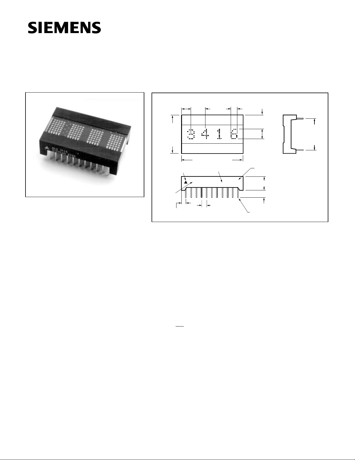
.270" 4-character 5 x 7 Dot Matrix
Alphanumeric Intelligent Display
with Memory/Decoder/Drive
Dimensions in inches (mm)
.157 (.40)
±.007 (.18)
.790
(20.07)
±.010
(.25)
Pin 1
Indicator
Part
No.
.145 (3.68) ±.015 (.38)
at Seating Plane
DESCRIPTION
The DLR/DLO/DLG3416 is a four character 5x7 dot matrix display module
with a built-in CMOS integrated circuit. This display is a “drop-in” replacement for the DL3416.
The integrated circuit contains memory, ASCII ROM decoder, multiplexing
circuitry and drivers. Data entry is asynchronous and can be random. A display system can be built using any number of DLX3416s since each character can be addressed independently and will continue to display the
character last stored until replaced by another.
System interconnection is very straightforward. The least significant two
address bits (A0, A1) are normally connected to the like-named inputs of all
displays in the system. With four chip enables, four displays (16 characters)
can easily be interconnected without a decoder.
Data lines are connected to all DLX3416s directly and in parallel, as is the
write line (WR
The cursor function causes all dots of a character position to illuminate at
half brightness. The cursor is not a character, and when removed the previously displayed character will reappear.
The DLX3416 has several features superior to competitive devices. True
“blanking” allows the designer to dim the display for more flexibility of display presentation. Finally the CLR clear function will clear the cursor RAM
and the ASCII character RAM simultaneously.
The character set consists of 128 special ASCII characters for English, German, Italian, Swedish, Danish, and Norwegian.
All products are subjected to out-going AQL’ s of 0.25% for brightness matching, visual alignment and dimensions, 0.065% for electrical and functional.
.325
(8.26)
1.300 (33.02) max
DLX3416
SIEMENS
). The display will then behave as a write-only memory.
.175
(4.45)
EIA Date Code
YYWW
.100 (2.54)
±.015 (38)
at Seating Plane
.260 (6.60)
±.007 (.18)
.270
(6.86)
Luminous
Intensity Code
Z
.160 (4.06) ±.020 (.51)
340 (8.64)
.020 (.51) x .012(.30)
Leads 22 pl.
.600 (15.24)
±.020 (.51)
at Seating
Plane
2–1
Page 2
2
2
1
1
C
C
C
V
V
V
V
V
V
N
Maximum Ratings
DC Supply Voltage....................–0.5 V to +7.0 Vdc
Input Voltage, Respect to GND
(all inputs).......................–0.5 V to V
Operating Temperature.................. -40 °
Storage Temperature-.................... 40 °
Relative Humidity at 85 °
C
+0.5 Vdc
CC
C to +85 ° C
C to +100 ° C
(non-condensing).........................................85%
Maximum Solder Temperature,
0.063" (1.59 mm) below
Seating Plane, t<5 sec .............................260 °
C
Optical Characteristics
Spectral Peak Wavelength
Red ..................................................660 nm typ.
HER ..................................................630 nm typ.
Green ...............................................565 nm typ.
Character Height0.270" (6.86 mm)
Time Averaged Luminous Intensity(1)
at V
=5 V
CC
Red............................................60 µ
HER..........................................120 µ
Green.......................................140 µ
cd/LED typ.
cd/LED typ.
cd/LED typ.
Dot to Dot Intensity Matching
at V
=5 V.......................................1.8:1.0 max.
CC
LED to LED Hue Matching
(Green only) at V
=5 V................... ± 2 nm max.
CC
Viewing Angle (off normal axis)
Horizontal ........................................... ±
Vertical . ............................................. ±
Note 1: Peak luminous intensity values can be calculated
by multiplying these values by 7.
50 ° max.
75 ° max.
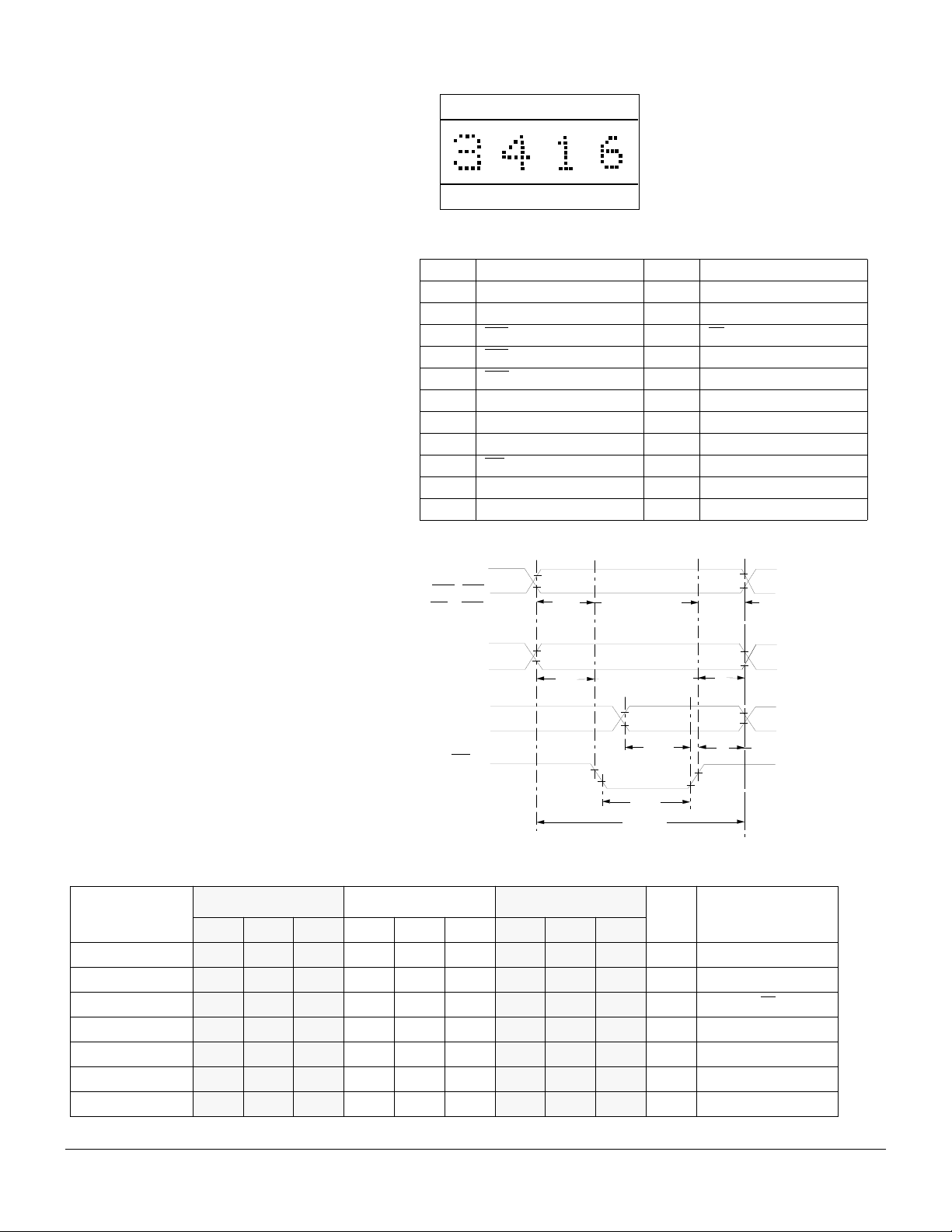
Figure 1. Top view
2 21 20 1918 17 16 15 14 13 1
digit 3 digit 2 digit 1 digit 0
2 3 4 5 6 7 8 9 10 1
Pin Function Pin Function
1 CE1 Chip Enable 12 GND
2 CE2 Chip Enable 13 NC
3 CE3 Chip Enable 14 BL Blanking
4 CE4 Chip Enable 15 NC
5 CLR Clear 16 D0 Data Input
6V
7 A0 Digit Select 18 D2 Data Input
8 A1 Digit Select 19 D3 Data Input
9WR Write 20 D4 Data Input
10 CU Cursor Select 21 D5 Data Input
11 CUE Cursor Select 22 D6 Data Input
CC
17 D1 Data Input
Figure 2. Timing characteristics, Write Cycle waveforms
E1, CE2
E3, C34
U, CLR
A0, A
T
ces
T
cus
T
clrd
1
T
as
T
ceh
T
cuh
T
ah
2.0 V
0.8 V
2.0
0.8
D0-D
WR
6
T
ds
2.0
0.8
T
dh
2.0
0.8
T
W
T
acc
ote: These waveforms are not edge triggered.
DC Characteristics
Parameter
Min. Typ. Max. Min. Typ. Max. Min. Typ. Max.
I
80 dots on 150 190 135 165 118 150 mA V
CC
I
Cursor 170 140 125 mA V
CC
I
Blank 2.8 4.0 2.3 3.0 2.0 2.5 mA V
CC
I
(all inputs) 30 60 120 25 50 100 20 40 80
IL
V
(all inputs) 2.0 2.0 2.0 VV
IH
V
(all inputs) 0.8 0.8 0.8 V V
IL
V
CC
4.5 5.0 5.5 4.5 5.0 5.5 4.5 5.0 5.5 V
–40 ° C +25 ° C +55 ° C
Units Conditions
=5 V
CC
=5 V
CC
=5 V, BL=0.8 V
CC
µ AV
=0.8 V, V
IN
=5 V
CC
=5 V
CC
CC
=5 V
2–2
DLR/DLO/DLG3416
Page 3
AC Characteristics Guaranteed Minimum Timing Parameters at
V
=5.0 V ± 0.5 V
CC
Parameter Symbol –40 ° C +25 ° C +85 ° C Units
Chip Enable Set Up Time T
Address Set Up Time T
Cursor Set Up Time T
Chip Enable Hold Time T
Address Hold Time T
Cursor Hold Time T
Clear Disable Time T
Write Time T
Data Set Up Time T
Data Hold Time T
Clear Time T
Access Time T
Note: 1. T
=Set Up Time + Write Time + Hold Time.
ACC
CES
AS
CUS
CEH
AH
CUH
CLRD
W
DS
DH
CLR
ACC
000ns
10 10 10 ns
10 10 10 ns
000ns
20 30 40 ns
20 30 40 ns
111
µ
s
60 70 90 ns
20 30 50 ns
20 30 40 ns
111
µ
s
90 110 140 ns
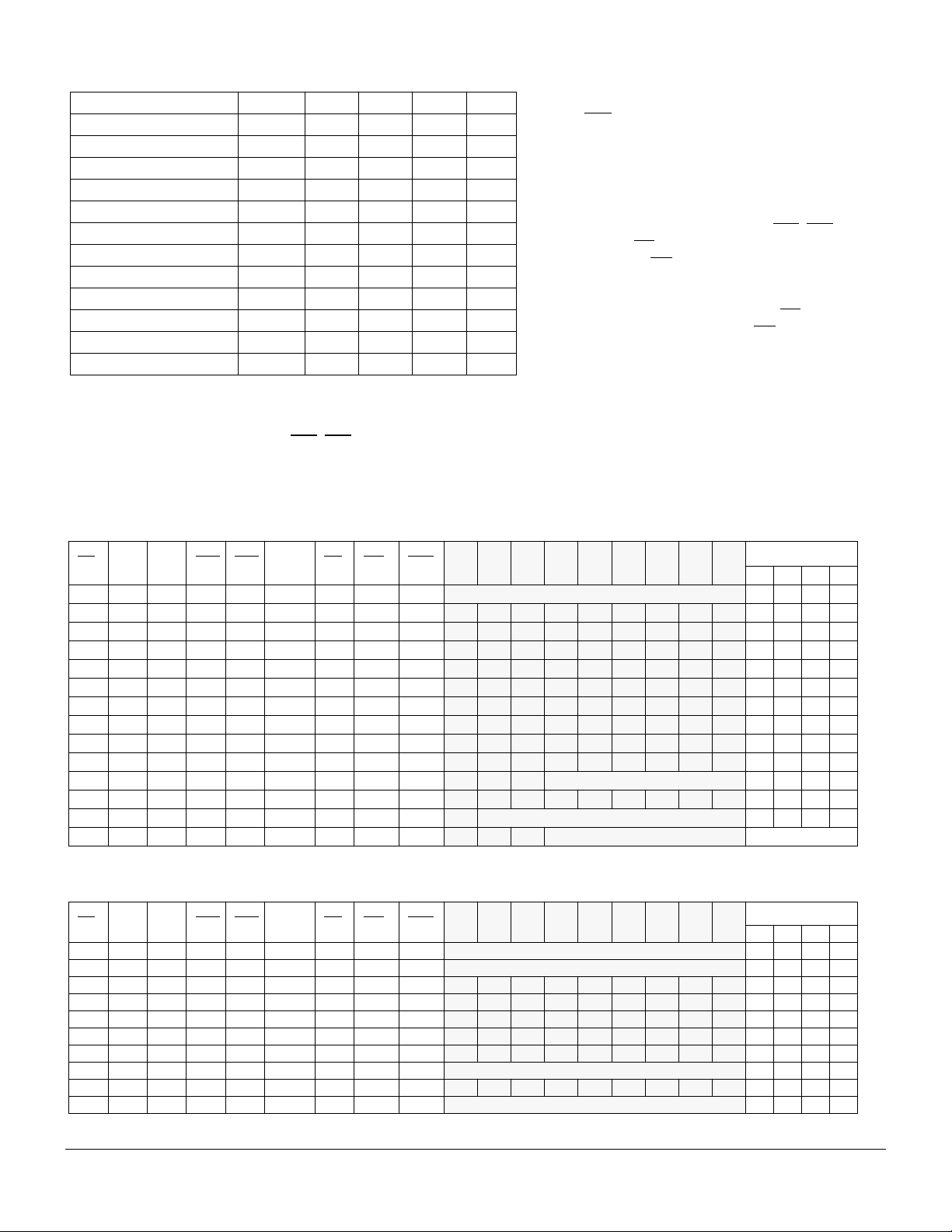
Loading Data
Setting the chip enable (CE1, CE2, CE3, CE4) to their true state will
enable loading. The desired data code (D0-D6) and digit address (A0,
A1) must be held stable during the write cycle for storing new data.
Data entry may be asynchronous and random. Digit 0
is defined as right hand digit with A1=A2=0.
To clear the entire internal four -digit memory hold the
clear (CLR
) low for 1 µ s. All illuminated dots will be
turned off within one complete display multiplex cycle,
1 msec minimum. The clear function will clear both the
ASCII RAM and the cursor RAM.
Loading Cursor
Setting the chip enables (CE1, CE2, CE3, CE4) and
cursor select (CU
loading. A write (WR
) to their true state will enable cursor
) pulse will now store or remove a
cursor into the digit location addressed by A0, A1, as
defined in data entry. A cursor will be stored if D0=1
and will removed if D0=0. The cursor (CU
should not be less than the write (WR
) pulse width
) pulse or errone-
ous data may appear in the display.
If the cursor is not required, the cursor enable signal
(CUE) may be tied low to disable the cursor function.
For a flashing cursor, simply pulse CUE. If the cursor
has been loaded to any or all positions in the display,
then CUE will control whether the cursor(s) or the
characters will appear. CUE does not affect the contents of cursor memory.
Typical Loading Data State Table
BL
CE1 CE2 CE3 CE4 CUE CU WR CLR A1 A0 D6 D5 D4 D3 D2 D1 D0
HXXXXL XH H previously loaded display G R E Y
HLXXXL XX H XXXXXXXXXGREY
HXLXXL XX H XXXXXXXXXGREY
HXXHXL XX H XXXXXXXXXGREY
HXXXHL XX H XXXXXXXXXGREY
HXXXXL XH H XXXXXXXXXGREY
HHHLL L HL H LLHLLLHLHGREE
HHHLL L HL H LHHLHLHLHGRUE
HHHLL L HL H HLHLLHHLLGLUE
HHHLL L HL H HHLLLLLHLBLUE
LXXXXX XH H XXL blank display
HHHLL L HL H HHLLLLHHHGLUE
HXXXXL XX L clears character display
HHHLL L HL H XX see character code see character set
X=don’t care
Digit
3210
Loading Cursor State Table
CE1 CE2 CE3 CE4 CUE CU WR CLR A1 A0 D6 D5 D4 D3 D2 D1 D0
BL
HXXXXL XH H previously loaded display B E A R
HXXXXH XH H display previously stored cursors B E A R
HHHLLH LL H LLXXXXXXHBEA ■
HHHLLH LL H LHXXXXXXHBE ■■
HHHLLH LL H HLXXXXXXHB ■■■
HHHLLH LL H HHXXXXXXH
HHHLLH LL H HLHLLLHLL
HXXXXL XH H disable cursor display B E A R
HHHLLL LL H HHXXXXXXLBEAR
HXXXXH XH H display stored cursors B E ■■
X=don’t care ■ =all dots on
Digit
3210
■■■■
■
E
■■
2–3
DLR/DLO/DLG3416
Page 4
V
h
1
0
V
h
1
0
D
D
D
D
D
D
D
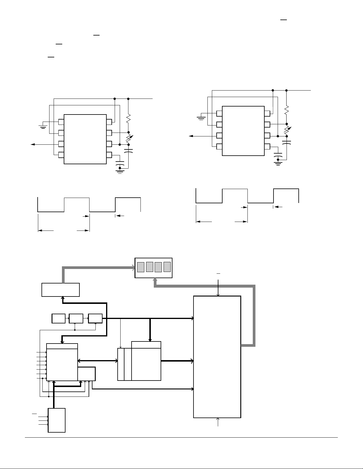
Display Blanking
Blank the display by loading a blank or space into each digit of
the display or by using the (BL
Setting the (BL
) input low does not affect the contents of either
) display blank input.
data or cursor memory. A flashing display can be achieved by
pulsing (BL
). A flashing circuit can be constructed using a 555
a stable multivibrator. Figure 3 illustrates a circuit in which varying R2 (100K~10K) will have a flash rate of 1 Hz~10 Hz.
Figure 3. Flashing circuit using a 555
VCC=5.0
R1
4.7 KΩ
R2
100 KΩ
C3
10 µF
To BL
Pin on
Display
C4
0.01 µF
8
7
6
5
1
2
3
4
555
Timer
Figure 3a. Flashing (blanking) timing
The display can be dimmed by pulsing (BL) line at a frequency
sufficiently fast to not interfere with the internal clock. The dimming signal frequency should be 2.5 KHz or higher. Dimming
the display also reduces power consumption.
An example of a simple dimming circuit using a 556 is illustrated in Figure 4. Adjusting potentiometer R3 will dim the display by changing the blanking pulse duty cycle.
Figure 4. Flashing circuit using a 555
VCC=5.0
R1
4.7 KΩ
R2
100 KΩ
C3
10 µF
To BL
Pin on
Display
C4
0.01 µF
8
7
6
5
1
2
3
4
555
Timer
Figure 4a. Flashing (blanking) timing
Blanking Pulse Widt
≈50% Duty Factor
~
500 ms
~
2 Hz Blanking Frequency
~
~
Blanking Pulse Widt
≈50% Duty Factor
~
500 ms
~
2 Hz Blanking Frequency
~
~
Figure 5. Internal block diagram
Display
Rows 0 to 6
3 2 1 0
Row Control Logic
&
Row Drivers
÷
128
÷
OSC
Counter
RAM Read Logic
6
5
4
3
2
1
0
WR
A0
A1
RAM
Memory
4 X 7 bit
Address Lines
Write
Address
Decoder
7
Counter
7 Bit ASCII Code
Cursor
Memory
4 X 1 bit
Timing and Control Logic
Row Decoder
ROM
128 X 35 Bit
ASCII
Character
Latches
Decode
Column Decoder
4480 bits
Cursor Memory Bits 0 to 3
Columns 0 to 19
Column Data
2–4
BL
Column Enable
Latches and
Column Drivers
CUE
DLR/DLO/DLG3416
Page 5
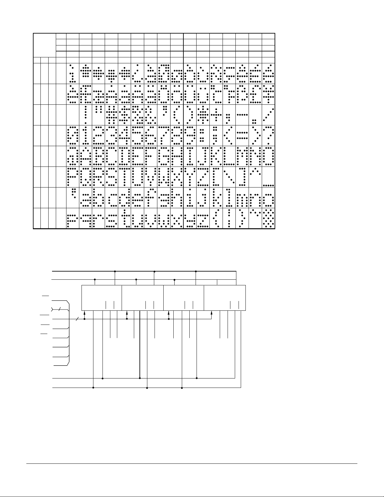
Character Set
1
.
D
D0
ASCII
CODE
D6 D5 D4 HEX
0
0
0
0
1
1
D1
D2
D3
0
0
0
1
1
0
1
1
0
0
0
1
0
1
0
0
0
0
0
0
0
1
0
0
1
2
3
4
5
1
1
1
0
0
0
0
2
3
1
0
0
0
1
1
0
0
5
4
1
0
1
1
1
1
0
0
7
6
1
0
0
0
0
0
1
1
9
8
1
0
1
1
0
0
1
1
B
A
1
0
0
0
1
1
1
1
D
C
1
0
1
1
1
1
1
1
F
E
1
1
0
6
1
1
1
7
. High=1 level. 2. Low=0 level. 3. Upon power up, device will initialize in a random state
Figure 6. Typical schematic, 16-character system
+V
GND
BL
0-DL
CLR
WR
CU
CUE
A
A
7
1
0
A
3
A
2
D15 D12 D11 D8 D7 D4 D3 D0
CE1
CE2
CE3
CE1
CE2
CE3
CE4
CE1
CE2
CE3
CE4
CE4
14
GND
GND
+V
GND
+V
GND
CE1
+V
CE2
+V
CE3
CE4
2–5
DLR/DLO/DLG3416
Page 6

Design Considerations
For details on design and applications of the DLX3416 using
standard bus configurations in multiple display systems, or parallel I/O devices, such as the 8255 with an 8080 or memory
mapped addressing on processors such as the 8080, Z80,
6502, or 6800, refer to Appnote 15 in the current Siemens Optoelectronics Data Book.
Electrical and Mechanical Considerations
V oltage Transient Suppression
We recommend that the same power supply be used for the
display and the components that interface with the display to
avoid logic inputs higher than V
. Additionally, the LEDs may
CC
cause transients in the power supply line while they change display states. The common practice is to place .01 mF capacitors
close to the displays across V
and GND, one for each dis-
CC
play, and one 10 mF capacitor for every second display .
ESD Protection
The silicon gate CMOS IC of the DLX3416 is quite resistant to
ESD damage and capable of withstanding discharges greater
than 2 KV. However, take all the standard precautions, normal
for CMOS components. These include properly grounding personnel, tools, tables, and transport carriers that come in contact
with unshielded parts. If these conditions are not, or cannot be
met, keep the leads of the device shorted together or the parts
in anti-static packaging.
Soldering Considerations
The DLX3416 can be hand soldered with SN63 solder using a
grounded iron set to 260 °
C.
Wave soldering is also possible following these conditions: Preheat that does not exceed 93 °
board or a package surface temperature of 85 °
C on the solder side of the PC
C. Water soluble
organic acid flux (except carboxylic acid) or resin-based RMA
flux without alcohol can be used.
Wave temperature of 245 °
C ± 5°C with a dwell between 1.5 sec.
to 3.0 sec. Exposure to the wave should not exceed temperatures above 260°C for five seconds at 0.063" below the seating
plane. The packages should not be immersed in the wave.
Post Solder Cleaning Procedures
The least offensive cleaning solution is hot D.I. water (60°C) for
less than 15 minutes. Addition of mild saponifiers is acceptable.
Do not use commercial dishwasher detergents.
For faster cleaning, solvents may be used. Carefully select any
solvent as some may chemically attack the nylon package.
Maximum exposure should not exceed two minutes at elevated
temperatures. Acceptable solvents are TF (trichorotribluorethane), TA, 111 Trichloroethane, and unheated acetone.
Note: Acceptable commercial solvents are: Basic TF, Arklone,
P. Genesolv , D. Genesolv DA, Blaco-Tron TF , Blaco-Tron TA, and
Freon TA.
Unacceptable solvents contain alcohol, methanol, methylene
chloride, ethanol, TP35, TCM, TMC, TMS+, TE, or TES. Since
many commercial mixtures exist, contact a solvent vendor for
chemical composition information. Some major solvent manufacturers are: Allied Chemical Corportation, Specialty Chemical
Division, Morristown, NJ; Baron-Blakeslee, Chicago, IL; Dow
Chemical, Midland, MI; E.I. DuPont de Nemours & Co., Wilmington, DE.
For further information refer to Siemens Appnotes 18 and 19.
An alternative to soldering and cleaning the display modules is
to use sockets. Standard pin DIP sockets .600" wide with
0.100" centers work well for single displays. Multiple display
assemblies are best handled by longer SIP sockets or DIP
sockets when available for uniform package alignment. Socket
manufacturers are Aries Electronics, Inc., Frenchtown, NJ;
Garry Manufacturing, New Brunswich, NJ; Robinson-Nugent,
New Albany , IN; and Samtec Electronic Har dware, New Albany,
IN.
For further information refer to Siemens Appnote 22.
Optical Considerations
The 0.270" high characters of the DLX3416 gives readability up
to eight feet. Proper filter selection enhances readability over
this distance.
Filters enhance the contrast ratio between a lit LED and the
character background intensifying the discrimination of different characters. The only limitation is cost. Take into consider ation the ambient lighting environment for the best cost/benefit
ratio for filters.
Incandescent (with almost no green) or fluorescent (with almost
no red) lights do not have the flat spectral response of sunlight.
Plastic band-pass filters are an inexpensive and effective way
to strengthen contrast ratios.
The DLR3416 is a standard red display and should be matched
with long wavelength pass filter in the 600 nm to 620 nm range.
The DLO3416 is a high efficiency red display and should be
matched with a long wavelength pass filter in the 470 nm to 590
range. The DLG3416 should be matched with a yellow-green
band-pass filter that peaks at 565 nm. For displays of multiple
colors, neutral density gray filters offer the best compromise.
Additional contrast enhancement is gained by shading the displays. Plastic band-pass filters with built-in louvers offer the
next step up in contrast improvement. Plastic filters can be
improved further with anti-reflective coatings to reduce glare.
The trade-off is fuzzy characters. Mounting the filters close to
the display reduces this effect. Take care not to overheat the
plastic filter by allowing for proper air flow.
Optimal filter enhancements are gained by using circular polarized, anti-reflective, band-pass filters. Circular polarizing further
enhances contrast by reducing the light that travels through the
filter and relfects back off the display to less than 1%.
Several filter manufacturers supply quality filter materials.
Some of them are: Panelgraphic Corporation, W. Caldwell, NJ;
SGL Homalite, Wilmington, DE; 3M Company, Visual Products
Division, St. Paul, MN; Polaroid Corporation, Polarizer Division,
Cambridge, MA; Marks Polarized Corporation, Deer Park, NY,
Hoya Optics, Inc., Fremont, CA.
One last note on mounting filters: recessing displays and bezel
assemblies is an inexpensive way to provide a shading effect in
overhead lighting situations. Several Bezel manufacturers are:
R.M.F. Products, Batavia, IL; Nobex Components, Griffith Plastic Corp., Burlingame, CA; Photo Chemical Products of California, Santa Monica, CA; .E.E.-Atlas, Van Nuys, CA.
Refer to Siemens Appnote 23 for further information.
2–6
DLR/DLO/DLG3416
 Loading...