

Page 1
Product
Folder
Order
Now
Technical
Documents
Tools &
Software
Support &
Community
DLPS013G –APRIL 2010–REVISED JANUARY 2019
DLP5500 DLP®0.55 XGA Series 450 DMD
DLP5500
1 Features
1
• 0.55-Inch Micromirror Array Diagonal
– 1024 × 768 Array of Aluminum, Micrometer-
Sized Mirrors (XGA Resolution)
– 10.8-µm Micromirror Pitch
– ±12° Micromirror Tilt Angle
(Relative to Flat State)
– Designed for Corner Illumination
• Designed for Use With Broadband Visible Light
(420 nm – 700 nm):
– Window Transmission 97% (Single Pass,
Through Two Window Surfaces)
– Micromirror Reflectivity 88%
– Array Diffraction Efficiency 86%
– Array Fill Factor 92%
• 16-Bit, Low Voltage Differential Signaling (LVDS)
Double Data Rate (DDR) Input Data Bus
• 200 MHz Input Data Clock Rate
• Dedicated DLPC200 Controller for High-Speed
Pattern Rates:
– 5,000 Hz (1-Bit Binary Patterns)
– 500 Hz (8-Bit Grayscale Patterns)
• Series 450 Package Characteristics:
– Thermal Area 18 mm × 12 mm Enabling High
on Screen Lumens (>2000 lm)
– 149 Micro Pin Grid Array Robust Electrical
Connection
– Package Mates to Amphenol InterCon
Systems 450-2.700-L-13.25-149 Socket
2 Applications
• Industrial
– 3D Scanners for Machine Vision and Quality
Control
– 3D Printing
– Direct Imaging Lithography
– Laser Marking and Repair
– Industrial and Medical Imaging
– Medical Instrumentation
– Digital Exposure Systems
• Medical
– Opthamology
– 3D Scanners for Limb and Skin Measurement
– Hyperspectral Imaging
• Displays
– 3D Imaging Microscopes
– Intelligent and Adaptive Lighting
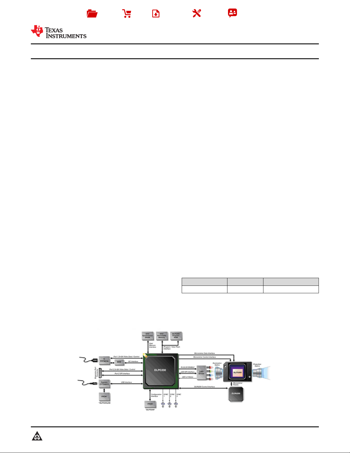
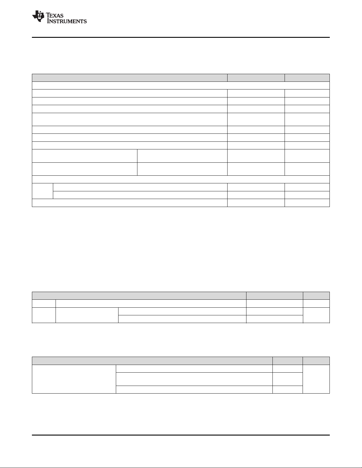
3 Description
Featuring over 750000 micromirrors, the high
resolution DLP5500 (0.55" XGA) digital micromirror
device (DMD) is a spatial light modulator (SLM) that
modulates the amplitude, direction, and/or phase of
incoming light. This advanced light control technology
has numerous applications in the industrial, medical,
and consumer markets. The DLP5500 enables fine
resolution for 3D printing applications.
Device Information
PART NUMBER PACKAGE BODY SIZE (NOM)
DLP5500 CPGA (149) 22.30 mm × 32.20 mm
(1) For all available packages, see the orderable addendum at
the end of the data sheet.
(1)
4 Typical Application Schematic
1
An IMPORTANT NOTICE at the end of this data sheet addresses availability, warranty, changes, use in safety-critical applications,
intellectual property matters and other important disclaimers. PRODUCTION DATA.
Page 2

DLP5500
DLPS013G –APRIL 2010–REVISED JANUARY 2019
www.ti.com
Table of Contents
1 Features.................................................................. 1
2 Applications ........................................................... 1
3 Description ............................................................. 1
4 Typical Application Schematic............................. 1
5 Revision History..................................................... 2
6 Description (continued)......................................... 4
7 Pin Configuration and Functions......................... 4
8 Specifications......................................................... 7
8.1 Absolute Maximum Ratings...................................... 7
8.2 Storage Conditions.................................................... 7
8.3 ESD Ratings.............................................................. 7
8.4 Recommended Operating Conditions....................... 8
8.5 Thermal Information................................................ 10
8.6 Electrical Characteristics......................................... 10
8.7 Timing Requirements.............................................. 11
8.8 System Mounting Interface Loads .......................... 15
8.9 Micromirror Array Physical Characteristics............. 16
8.10 Micromirror Array Optical Characteristics............. 17
8.11 Window Characteristics......................................... 18
8.12 Chipset Component Usage Specification ............. 18
9 Detailed Description............................................ 19
9.1 Overview................................................................. 19
9.2 Functional Block Diagram....................................... 20
9.3 Feature Description................................................. 21
9.4 Device Functional Modes........................................ 24
9.5 Window Characteristics and Optics ....................... 24
9.6 Micromirror Array Temperature Calculation............ 25
9.7 Micromirror Landed-on/Landed-Off Duty Cycle...... 27
10 Application and Implementation........................ 29
10.1 Application Information.......................................... 29
10.2 Typical Application................................................ 30
11 Power Supply Recommendations ..................... 32
11.1 DMD Power-Up and Power-Down Procedures..... 32
12 Layout................................................................... 32
12.1 Layout Guidelines ................................................. 32
12.2 Layout Example .................................................... 33
13 Device and Documentation Support................. 34
13.1 Device Support .................................................... 34
13.2 Documentation Support ........................................ 34
13.3 Related Documentation......................................... 34
13.4 Community Resources.......................................... 34
13.5 Trademarks........................................................... 35
13.6 Electrostatic Discharge Caution............................ 35
13.7 Glossary................................................................ 35
14 Mechanical, Packaging, and Orderable
Information........................................................... 35
5 Revision History
Changes from Revision F (May 2015) to Revision G Page
• Changed DMD Marking Image Object for Figure 19 ........................................................................................................... 34
Changes from Revision E (September 2013) to Revision F Page
• Added ESD Ratings, Feature Description section, Device Functional Modes, Application and Implementation
section, Power Supply Recommendations section, Layout section, Device and Documentation Support section, and
Mechanical, Packaging, and Orderable Information section ................................................................................................. 1
• Changed Incorrect V
• Changed LVDS ƒ
• Added Max Recommended DMD Temperature – Derating Curve......................................................................................... 9
• Added LVCMOS Output Measurement Condition Figure..................................................................................................... 10
• Changed Incorrect tCvalue from 4 ns to 5 ns (200 MHz clock) ........................................................................................... 11
• Changed Incorrect tWvalue from 1.25 ns to 2.5 ns (200 MHz clock)................................................................................... 11
• Changed SCP Bus Diagrams............................................................................................................................................... 11
• Added LVDS Voltage Definition Figure ................................................................................................................................ 12
• Changed LVDS Waveform Requirements Figure................................................................................................................. 13
• Added LVDS Equivalent Input Circuit Figure ....................................................................................................................... 13
• Added LVDS & SCP Rise and Fall Time Figures................................................................................................................. 14
• Moved the Mechanical section from Recommended Operating Conditions table to the System Mounting Interface
Loads section ...................................................................................................................................................................... 15
• Added Micromirror Array Physical Characteristics section .................................................................................................. 16
• Changed Micromirror Array Physical Characteristics Figure to generic image (M x N)....................................................... 16
value from 9V to 8V......................................................................................................................... 7
CC2
to200 MHz - previously incorrectly listed as 150 MHz......................................................................... 9
clock
2
Submit Documentation Feedback Copyright © 2010–2019, Texas Instruments Incorporated
Product Folder Links: DLP5500
Page 3

DLP5500
www.ti.com
• Added Micromirror Array Optical Characteristics section .................................................................................................... 17
• Changed specular reflectivity wavelength range to 420 - 700 nm (from 400 - 700 nm) to match Recommended
Operating Conditions............................................................................................................................................................ 17
• Changed Micromirror Landed Orientation and Tilt Figure to generic image (M x N) ........................................................... 18
• Added Window Characteristics section ............................................................................................................................... 18
• Added Chipset Component Usage Specification section .................................................................................................... 18
• Changed Micromirror Array, Pitch, Hinge Axis Orientation Figure to generic image (M x N).............................................. 22
• Changed Micromirror States: On, Off, Flat Figure to generic DMD image .......................................................................... 23
• Changed Test Point locations from TC1 & TC2 to TP1 - TP5 ............................................................................................. 25
• Changed Test Point location Diagram to show TP1 - TP5................................................................................................... 26
• Added Micromirror Landed-on/Landed-Off Duty Cycle section............................................................................................ 27
• Changed Typical Application diagram.................................................................................................................................. 30
• Replaced "DAD" with "DLPA200"......................................................................................................................................... 31
Changes from Revision D (October 2012) to Revision E Page
• Deleted the Device Part Number Nomenclature section...................................................................................................... 34
Changes from Revision C (June 2012) to Revision D Page
DLPS013G –APRIL 2010–REVISED JANUARY 2019
• Changed the Device Part Number Nomenclature From: DLP5500FYA To: DLP5500AFYA............................................... 34
• Updated Mechanical ICD to V2 with a minor change in the window height......................................................................... 34
Changes from Revision B (Spetember 2011) to Revision C Page
• Added the Package Footprint and Socket information in the Features list ........................................................................... 1
• Deleted redundant information from the Description.............................................................................................................. 1
• Changed the Illumination power density Max value of <420 mm From: 20 To: 2 mW/cm2................................................... 7
• Changed Storage temperature range and humidity values in Absolute Maximum Ratings .................................................. 7
• Added Operating Case Temperature, Operating Humidity, Operating Device Temperature Gradient and Operating
Landed Duty-Cycle to RECOMMENDED OPERATING CONDITIONS................................................................................. 8
• Added Mirror metal specular reflectivity and Illumination overfill values to "Micromirror Array Optical Characteristics"
table...................................................................................................................................................................................... 17
• Corrected the C
, Qarray and T
L2W
values in Micromirror Array Temperature Calculation for Uniform Illumination. ...... 26
array
• Corrected the document reference in Related Documents section...................................................................................... 34
Changes from Revision A (June 2010) to Revision B Page
• Changed the window refractive index NOM spec From: 1.5090 To: 1.5119 ....................................................................... 17
• Added table note "At a wavelength of 632.8 nm"................................................................................................................. 17
Changes from Original (April 2010) to Revision A Page
• Changed V
REF
to V
............................................................................................................................................................. 7
CC1
• Added |VID| to the absolute max table.................................................................................................................................... 7
• Added V
to the absolute max table................................................................................................................................ 7
MBRST
• Clarified Note6 measurement point ....................................................................................................................................... 7
• Changed the Illumination power density Max value of <420 mm From: 2 To: 20 mW/cm2................................................... 7
• Added Additional Related Documents.................................................................................................................................. 34
Submit Documentation FeedbackCopyright © 2010–2019, Texas Instruments Incorporated
Product Folder Links: DLP5500
3
Page 4
DLP5500
DLPS013G –APRIL 2010–REVISED JANUARY 2019
www.ti.com
6 Description (continued)
The XGA resolution has the direct benefit of scanning large objects for 3D machine vision applications. Reliable
function and operation of the DLP5500 requires that it be used in conjunction with the DLPC200 digital controller
and the DLPA200 analog driver. This dedicated chipset provides a robust, high resolution XGA, and high speed
system solution.
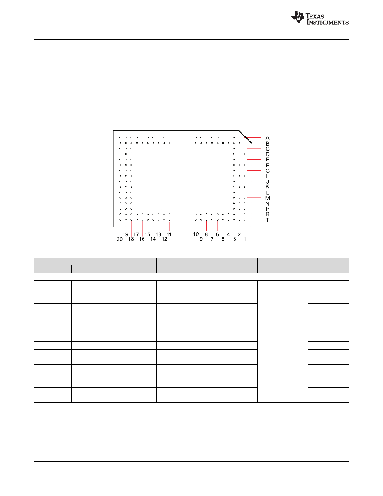
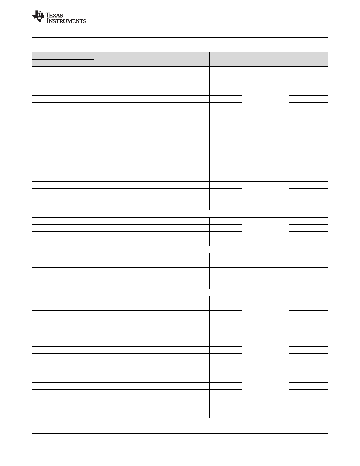
7 Pin Configuration and Functions
FYA Package
149-Pin CPGA Series 450
Bottom View
(1)
Pin Functions
PIN
NAME NO.
DATA INPUTS
D_AN1 G20 Input LVCMOS DDR Differential DCLK_A
D_AP1 H20 Input LVCMOS DDR Differential DCLK_A 744
D_AN3 H19 Input LVCMOS DDR Differential DCLK_A 688
D_AP3 G19 Input LVCMOS DDR Differential DCLK_A 703
D_AN5 F18 Input LVCMOS DDR Differential DCLK_A 686
D_AP5 G18 Input LVCMOS DDR Differential DCLK_A 714
D_AN7 E18 Input LVCMOS DDR Differential DCLK_A 689
D_AP7 D18 Input LVCMOS DDR Differential DCLK_A 705
D_AN9 C20 Input LVCMOS DDR Differential DCLK_A 687
D_AP9 D20 Input LVCMOS DDR Differential DCLK_A 715
D_AN11 B18 Input LVCMOS DDR Differential DCLK_A 715
D_AP11 A18 Input LVCMOS DDR Differential DCLK_A 732
D_AN13 A20 Input LVCMOS DDR Differential DCLK_A 686
D_AP13 B20 Input LVCMOS DDR Differential DCLK_A 715
D_AN15 B19 Input LVCMOS DDR Differential DCLK_A 700
D_AP15 A19 Input LVCMOS DDR Differential DCLK_A 719
(1) The following power supplies are required to operate the DMD: VCC, VCCI, VCC2. VSS must also be connected.
(2) DDR = Double Data Rate. SDR = Single Data Rate. Refer to the Timing Requirements for specifications and relationships.
(3) Refer to Electrical Characteristics for differential termination specification.
(4) Internal Trace Length (mils) refers to the Package electrical trace length. See the DLP®0.55 XGA Chip-Set Data Manual (DLPZ004) for
details regarding signal integrity considerations for end-equipment designs.
4
Submit Documentation Feedback Copyright © 2010–2019, Texas Instruments Incorporated
TYPE
(I/O/P )
SIGNAL
DATA
RATE
INTERNAL
(2)
TERM
(3)
Product Folder Links: DLP5500
CLOCK DESCRIPTION
Input data bus A
(LVDS)
TRACE
(mils)
715
(4)
Page 5
www.ti.com
DLPS013G –APRIL 2010–REVISED JANUARY 2019
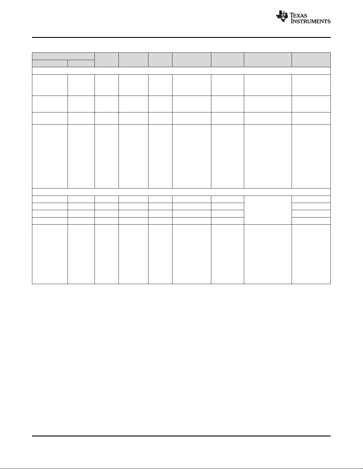
Pin Functions (continued)
(1)
PIN
NAME NO.
D_BN1 K20 Input LVCMOS DDR Differential DCLK_B
D_BP1 J20 Input LVCMOS DDR Differential DCLK_B 745
D_BN3 J19 Input LVCMOS DDR Differential DCLK_B 686
D_BP3 K19 Input LVCMOS DDR Differential DCLK_B 703
D_BN5 L18 Input LVCMOS DDR Differential DCLK_B 686
D_BP5 K18 Input LVCMOS DDR Differential DCLK_B 714
D_BN7 M18 Input LVCMOS DDR Differential DCLK_B 693
D_BP7 N18 Input LVCMOS DDR Differential DCLK_B 709
D_BN9 P20 Input LVCMOS DDR Differential DCLK_B 687
D_BP9 N20 Input LVCMOS DDR Differential DCLK_B 715
D_BN11 R18 Input LVCMOS DDR Differential DCLK_B 702
D_BP11 T18 Input LVCMOS DDR Differential DCLK_B 719
D_BN13 T20 Input LVCMOS DDR Differential DCLK_B 686
D_BP13 R20 Input LVCMOS DDR Differential DCLK_B 715
D_BN15 R19 Input LVCMOS DDR Differential DCLK_B 680
D_BP15 T19 Input LVCMOS DDR Differential DCLK_B 700
DCLK_AN D19 Input LVCMOS - Differential –
DCLK_AP E19 Input LVCMOS - Differential – 728
DCLK_BN N19 Input LVCMOS - Differential –
DCLK_BP M19 Input LVCMOS - Differential – 728
DATA CONTROL INPUTS
SCTRL_AN F20 Input LVCMOS DDR Differential DCLK_A
SCTRL_AP E20 Input LVCMOS DDR Differential DCLK_A 731
SCTRL_BN L20 Input LVCMOS DDR Differential DCLK_B 707
SCTRL_BP M20 Input LVCMOS DDR Differential DCLK_B 722
SERIAL COMMUNICATION (SCP) AND CONFIGURATION
SCP_CLK A8 Input LVCMOS – Pull-Down – –
SCP_DO A9 Output LVCMOS – – SCP_CLK –
SCP_DI A5 Input LVCMOS – Pull-Down SCP_CLK –
SCP_EN B7 Input LVCMOS – Pull-Down SCP_CLK –
PWRDN B9 Input LVCMOS – Pull-Down – –
MICROMIRROR BIAS CLOCKING PULSE
MODE_A A4 Input LVCMOS – Pull-Down – –
MBRST0 C3 Input Analog – – –
MBRST1 D2 Input Analog – – – –
MBRST2 D3 Input Analog – – – –
MBRST3 E2 Input Analog – – – –
MBRST4 G3 Input Analog – – – –
MBRST5 E1 Input Analog – – – –
MBRST6 G2 Input Analog – – – –
MBRST7 G1 Input Analog – – – –
MBRST8 N3 Input Analog – – – –
MBRST9 M2 Input Analog – – – –
MBRST10 M3 Input Analog – – – –
MBRST11 L2 Input Analog – – – –
MBRST12 J3 Input Analog – – – –
MBRST13 L1 Input Analog – – – –
MBRST14 J2 Input Analog – – – –
MBRST15 J1 Input Analog – – – –
TYPE
(I/O/P )
SIGNAL
DATA
RATE
INTERNAL
(2)
TERM
(3)
CLOCK DESCRIPTION
Input data bus B
(LVDS)
Input data bus A Clock
(LVDS)
Input data bus B Clock
(LVDS)
Data Control (LVDS)
Micromirror Bias
Clocking Pulse
"MBRST" signals
"clock" micromirrors
into state of LVCMOS
memory cell associated
with each mirror.
DLP5500
TRACE
(4)
(mils)
716
700
700
716
–
Product Folder Links: DLP5500
Submit Documentation FeedbackCopyright © 2010–2019, Texas Instruments Incorporated
5
Page 6
DLP5500
DLPS013G –APRIL 2010–REVISED JANUARY 2019
Pin Functions (continued)
(1)
PIN
NAME NO.
POWER
B11,B12,B1
V
CC
3,B16,R12,
R13,R16,R1
7
A12,A14,A1
V
CCI
V
CC2
6,T12,T14,T16Power Analog – – –
C1,D1,M1,N
1
A6,A11,A13,
A15,A17,B4,
B5,B8,B14,
B15,B17,C2
,C18,C19,F
1,F2,F19,H1
V
SS
,H2,H3,H18,
J18,K1,K2,L
19,N2,P18,
P19,R4,R9,
R14,R15,T7
,T13,T15,T1
7
RESERVED SIGNALS (Not for use in system)
RESERVED_R7 R7 Input LVCMOS – Pull-Down –
RESERVED_R8 R8 Input LVCMOS – Pull-Down – –
RESERVED_T8 T8 Input LVCMOS – Pull-Down – –
RESERVED_B6 B6 Input LVCMOS – Pull-Down – –
A3, A7,
A10, B2,
B3, B10,
E3, F3, K3,
L3, P1, P2,
NO_CONNECT
P3, R1, R2,
R3, R5, R6,
R10, R11,
T1, T2, T3,
T4, T5, T6,
T9, T10,
T11
TYPE
(I/O/P )
SIGNAL
Power Analog – – –
DATA
RATE
INTERNAL
(2)
TERM
(3)
CLOCK DESCRIPTION
Power for LVCMOS
Logic
Power supply for LVDS
Interface
Power Analog – – –
Power Analog – – –
Power for High Voltage
CMOS Logic
Common return for all
power inputs
Pins should be
connected to V
SS
– – – – – DO NOT CONNECT –
www.ti.com
TRACE
(4)
(mils)
–
–
–
–
–
6
Submit Documentation Feedback Copyright © 2010–2019, Texas Instruments Incorporated
Product Folder Links: DLP5500
Page 7
DLP5500
www.ti.com
DLPS013G –APRIL 2010–REVISED JANUARY 2019
8 Specifications
8.1 Absolute Maximum Ratings
over operating free-air temperature range (unless otherwise noted)
ELECTRICAL
V
CC
V
CCI
Voltage applied to V
Voltage applied to V
Delta supply voltage |VCC– V
|VID|
V
CC2
V
MBRST
Maximum differential voltage, Damage can occur to internal resistor if exceeded,
See Figure 6
Voltage applied to V
Voltage applied to MBRST[0:15] Input Pins –28 28 V
Voltage applied to all other pins
I
OH
I
OL
Current required from a high-level
output
Current required from a low-level
output
ENVIRONMENTAL
T
CASE
Case temperature: operational
Case temperature: non–operational
Dew Point (Operating and non-Operating) 81 ºC
(1) Stresses beyond those listed under Absolute Maximum Ratings may cause permanent damage to the device. These are stress ratings
only, which do not imply functional operation of the device at these or any other conditions beyond those indicated under Recommended
Operating Conditions. Exposure to absolute-maximum-rated conditions for extended periods may affect device reliability.
(2) All voltages referenced to VSS(ground).
(3) Voltages VCC, V
(4) Exceeding the recommended allowable absolute voltage difference between VCCand V
CCI
, and V
difference between VCCand V
(5) Exposure of the DMD simultaneously to any combination of the maximum operating conditions for case temperature, differential
temperature, or illumination power density (see Recommended Operating Conditions).
(6) DMD Temperature is the worst-case of any test point shown in Figure 16, or the active array as calculated by the Micromirror Array
Temperature Calculation.
(2)(3)
CC
(2)(3)
CCI
OFFSET
CCI
(2)(3)(4)
(4)
|
(2)
VOH= 2.4 V –20 mA
VOL= 0.4 V 15 mA
(5) (6)
(6)
are required for proper DMD operation.
CC2
, | VCC- V
CCI
|, should be less than .3V.
CCI
(1)
MIN MAX UNIT
–0.5 4 V
–0.5 4 V
0.3 V
700 mV
–0.5 8 V
–0.5 VCC+ 0.3 V
–20 90 ºC
–40 90 ºC
may result in excess current draw. The
CCI
8.2 Storage Conditions
applicable before the DMD is installed in the final product
MIN MAX UNIT
T
stg
T
DP
(1) Long-term is defined as the usable life of the device.
(2) Dew points beyond the specified long-term dew point are for short-term conditions only, where short-term is defined as less than 60
DMD storage temperature –40 80 °C
Storage dew point
Storage Dew Point - long-term
Storage Dew Point - short-term
(1)
(2)
cumulative days over the usable life of the device (operating, non-operating, or storage).
24
28
°C
8.3 ESD Ratings
VALUE UNIT
Electrostatic discharge immunity for LVCMOS [I/O] pins
V
(ESD)
Electrostatic discharge
Human body model (HBM), per ANSI/ESDA/JEDEC JS-001, all other
pins [power, control pins] except MBRST
(2)
Electrostatic discharge immunity for MBRST[0:15] pins
(1) Tested in accordance with JESD22-A114-B Electrostatic Discharge (ESD) sensitivity testing Human Body Model (HBM).
(2) JEDEC document JEP155 states that 500-V HBM allows safe manufacturing with a standard ESD control process.
Product Folder Links: DLP5500
(1)
±2000
±2000
(1)
<250
Submit Documentation FeedbackCopyright © 2010–2019, Texas Instruments Incorporated
V
7
Page 8
DLP5500
DLPS013G –APRIL 2010–REVISED JANUARY 2019
www.ti.com
8.4 Recommended Operating Conditions
over operating free-air temperature range (unless otherwise noted)
SUPPLY VOLTAGES
V
CC
V
CCI
V
CC2
|V
V
| Supply voltage delta (absolute value)
CCI–VCC
MBRST
(1) (2)
Supply voltage for LVCMOS core logic 3.15 3.3 3.45 V
Supply voltage for LVDS receivers 3.15 3.3 3.45 V
Mirror electrode and HVCMOS supply voltage 8.25 8.5 8.75 V
(3)
Micromirror clocking pulse voltages -27 26.5 V
LVCMOS PINS
V
IH
V
IL
I
OH
I
OL
T
PWRDNZ
High level Input voltage
Low level Input voltage
High level output current at VOH= 2.4 V –20 mA
Low level output current at VOL= 0.4 V 15 mA
PWRDNZ pulse width
(4)
(4)
(5)
SCP INTERFACE
ƒ
clock
t
SCP_SKEW
t
SCP_DELAY
t
SCP_BYTE_INTERVAL
t
SCP_NEG_ENZ
t
SCP_PW_ENZ
t
SCP_OUT_EN
ƒ
clock
SCP clock frequency
Time between valid SCPDI and rising edge of SCPCLK
Time between valid SCPDO and rising edge of SCPCLK
Time between consecutive bytes 1 µs
Time between falling edge of SCPENZ and the first rising edge of SCPCLK 30 ns
SCPENZ inactive pulse width (high level) 1 µs
Time required for SCP output buffer to recover after SCPENZ (from tri-state) 1.5 ns
SCP circuit clock oscillator frequency
(6)
(7)
(7)
(8)
(1) Supply voltages VCC, VCCI, VOFFSET, VBIAS, and VRESET are all required for proper DMD operation. VSS must also be connected.
(2) VOFFSET supply transients must fall within specified max voltages.
(3) To prevent excess current, the supply voltage delta |VCCI – VCC| must be less than specified limit.
(4) Tester Conditions for VIHand VIL:
Frequency = 60MHz. Maximum Rise Time = 2.5 ns at (20% to 80%)
Frequency = 60MHz. Maximum Fall Time = 2.5 ns at (80% to 20%)
(5) PWRDNZ input pin resets the SCP and disables the LVDS receivers. PWRDNZ input pin overrides SCPENZ input pin and tri-states the
SCPDO output pin.
(6) The SCP clock is a gated clock. Duty cycle shall be 50% ± 10%. SCP parameter is related to the frequency of DCLK.
(7) Refer to Figure 3.
(8) SCP internal oscillator is specified to operate all SCP registers. For all SCP operations, DCLK is required.
MIN NOM MAX UNIT
0.3 V
1.7 2.5 VCC + 0.15 V
– 0.3 0.7 V
10 ns
500 kHz
–800 800 ns
700 ns
9.6 11.1 MHz
8
Submit Documentation Feedback Copyright © 2010–2019, Texas Instruments Incorporated
Product Folder Links: DLP5500
Page 9
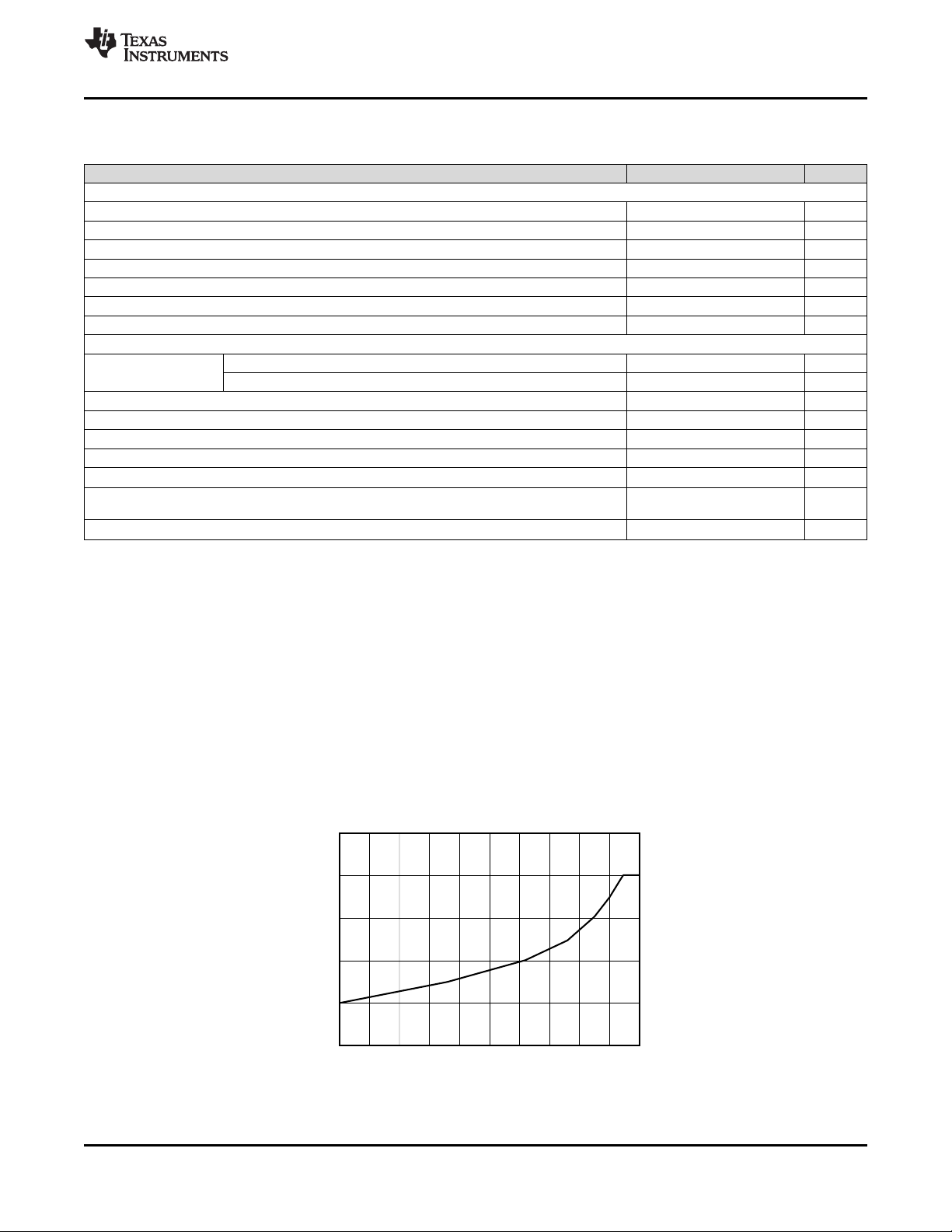
Micromirror Landed Duty Cycle
Operational (°C)
0/100 5/95 10/90 15/85 20/80 25/75 30/70 35/65 40/60 45/55
30
40
50
60
70
80
D001
50/50
100/0 95/5 90/10 85/15 80/20 75/25 70/30 65/35 60/40 55/45
Max Recommended Array Temperature –
DLP5500
www.ti.com
DLPS013G –APRIL 2010–REVISED JANUARY 2019
Recommended Operating Conditions (continued)
over operating free-air temperature range (unless otherwise noted)
MIN NOM MAX UNIT
LVDS INTERFACE
ƒ
clock
|VID| Input differential voltage (absolute value)
V
CM
V
LVDS
t
LVDS_RSTZ
Z
IN
Z
LINE
ENVIRONMENTAL
T
DMD
T
WINDOW
T
CERAMIC-WINDOW-DELTA
ILL
UV
ILL
VIS
ILL
IR
(9) Refer to Figure 5, Figure 6, and Figure 7.
(10) Optimal, long-term performance and optical efficiency of the Digital Micromirror Device (DMD) can be affected by various application
parameters, including illumination spectrum, illumination power density, micromirror landed duty-cycle, ambient temperature (storage
and operating), DMD temperature, ambient humidity (storage and operating), and power on or off duty cycle. TI recommends that
application-specific effects be considered as early as possible in the design cycle.
(11) DMD Temperature is the worst-case of any thermal test point in Figure 16, or the active array as calculated by the Micromirror Array
Temperature Calculation for Uniform Illumination.
(12) Per Figure 1, the maximum operational case temperature should be derated based on the micromirror landed duty cycle that the DMD
experiences in the end application. Refer to Micromirror Landed-on/Landed-Off Duty Cycle for a definition of micromirror landed duty
cycle.
(13) Long-term is defined as the average over the usable life of the device.
(14) Short-term is defined as less than 60 cumulative days over the over the usable life of the device.
(15) Window temperature as measured at thermal test points TP2, TP3, TP4 and TP5 in Figure 16.The locations of thermal test points TP2,
TP3, TP4 and TP5 in Figure 16 are intended to measure the highest window edge temperature. If a particular application causes
another point on the window edge to be at a higher temperature, a test point should be added to that location.
(16) Ceramic package temperature as measured at test point 1 (TP 1) in Figure 16.
(17) Dew points beyond the specified long-term dew point (operating, non-operating, or storage) are for short-term conditions only, where
short-term is defined as< 60 cumulative days over the usable life of the device.
(18) Refer to Thermal Information and Micromirror Array Temperature Calculation.
Clock frequency for LVDS interface, DCLK (all channels) 200 MHz
Common mode
LVDS voltage
(9)
(9)
(9)
100 400 600 mV
1200 mV
0 2000 mV
Time required for LVDS receivers to recover from PWRDNZ 10 ns
Internal differential termination resistance 95 105 Ω
Line differential impedance (PWB/trace) 90 100 110 Ω
(10)
(15)
(11) (12) (13)
(11) (14)
10 40 to 70
–20 75 °C
(15) (16)
Long-term DMD temperature (operational)
Short-term DMD temperature (operational)
Window temperature – operational
Delta ceramic-to-window temperature -operational
Long-term dew point (operational & non-operational) 24 °C
Short-term dew point
(13) (17)
(operational & non-operational) 28 °C
Illumination, wavelength < 420 nm 0.68
Illumination, wavelengths between 420 and 700 nm
Thermally
Limited
Illumination, wavelength > 700 nm 10
(12)
90 °C
30 °C
mW/cm
mW/cm
(18)
mW/cm
°C
2
2
2
Figure 1. Max Recommended DMD Temperature – Derating Curve
Product Folder Links: DLP5500
Submit Documentation FeedbackCopyright © 2010–2019, Texas Instruments Incorporated
9
Page 10
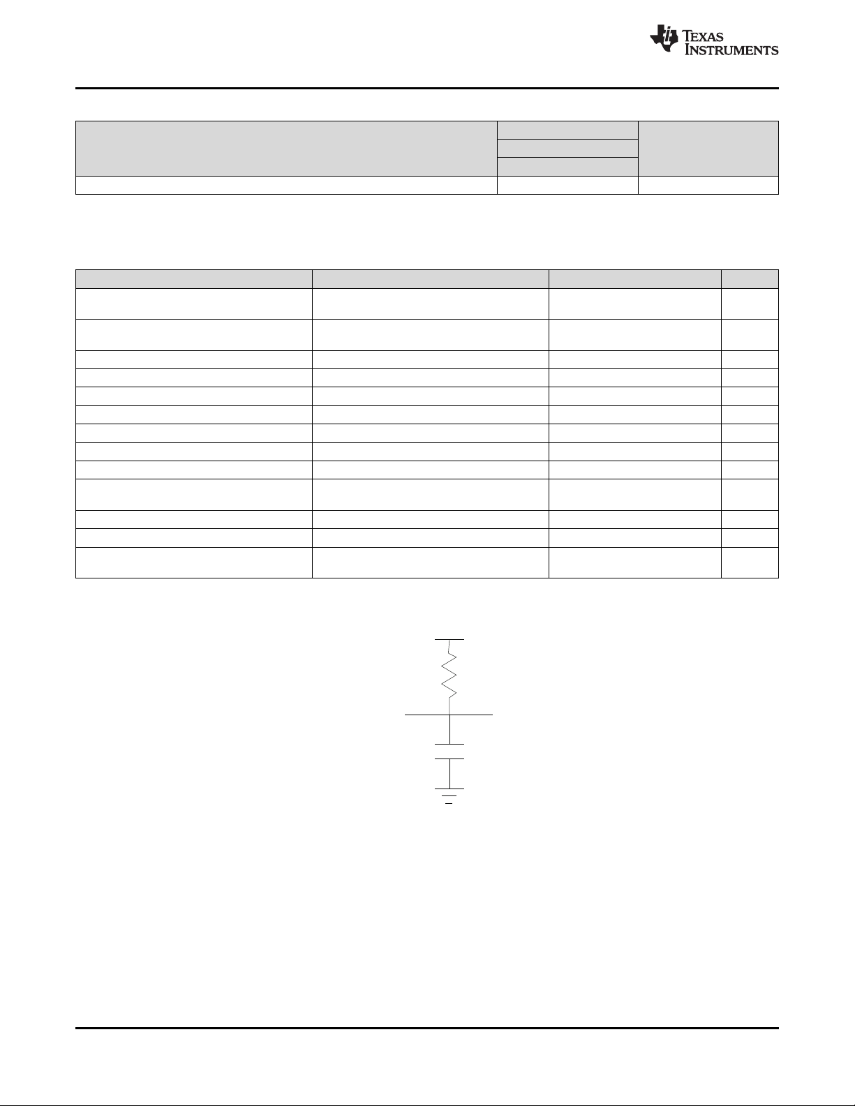
From Output
Under Test
Tester
Channel
LOAD CIRCUIT
C = 50 pF
C = 5 pF for Disable Time
L
L
R
L
DLP5500
DLPS013G –APRIL 2010–REVISED JANUARY 2019
8.5 Thermal Information
THERMAL METRIC
Thermal resistance from active array to specified point on case (TP1)
(1)
(1) For more information, see Micromirror Array Temperature Calculation.
8.6 Electrical Characteristics
over operating free-air temperature range (unless otherwise noted)
PARAMETER TEST CONDITIONS MIN TYP MAX UNIT
V
V
I
I
I
I
I
I
Z
Z
C
C
C
OH
OL
OZ
IL
IH
CC
CCI
CC2
IN
LINE
I
O
IM
High-level output voltage
Figure 2
Low-level output voltage
Figure 2
High impedance output current
Low-level input current
High-level input current
Current into VCCpin VCC= 3.6 V, 750 mA
Current into V
Current into V
OFFSET
CC2
Internal Differential Impedance 95 105 Ω
Line Differential Impedance (PWB
or Trace)
Input capacitance
Output capacitance
Input capacitance for
MBRST[0:15] pins
(1) Applies to LVCMOS pins only
(2) Exceeding the maximum allowable absolute voltage difference between VCCand V
Absolute Maximum Ratings for details)
(1)
, See
(1)
, See
(1)
(1)
(1)
(2)
pin
pin V
(1)
(1)
VCC= 3.0 V, IOH= –20 mA 2.4 V
VCC= 3.6 V, IOL= 15 mA 0.4 V
VCC= 3.6 V 10 µA
VCC= 3.6 V, VI= 0 V –60 µA
VCC= 3.6 V, VI= V
V
= 3.6 V 450 mA
CCI
= 8.75V 25 mA
CC2
CC
f = 1 MHz 10 pF
f = 1 MHz 10 pF
f = 1 MHz 160 210 pF
DLP5500
UNITFYA (CPGA)
149 PINS
0.6 °C/W
200 µA
90 100 110 Ω
may result in excess current draw. (Refer to
CCI
www.ti.com
10
Figure 2. Measurement Condition for LVCMOS Output
Submit Documentation Feedback Copyright © 2010–2019, Texas Instruments Incorporated
Product Folder Links: DLP5500
Page 11
50% 50%
t
c
f
clock
= 1 / t
c
SCPCLK
SCPDI
50%
t
SCP_SKEW
SCPD0
50%
t
SCP_DELAY
DLP5500
www.ti.com
DLPS013G –APRIL 2010–REVISED JANUARY 2019
8.7 Timing Requirements
over operating free-air temperature range (unless otherwise noted)
MIN NOM MAX UNIT
LVDS TIMING PARAMETERS (See Figure 9)
t
c
t
w
t
s
t
s
t
h
t
h
t
skew
LVDS WAVEFORM REQUIREMENTS (See Figure 6)
|VID| Input Differential Voltage (absolute difference) 100 400 600 mV
V
CM
V
LVDS
t
r
t
r
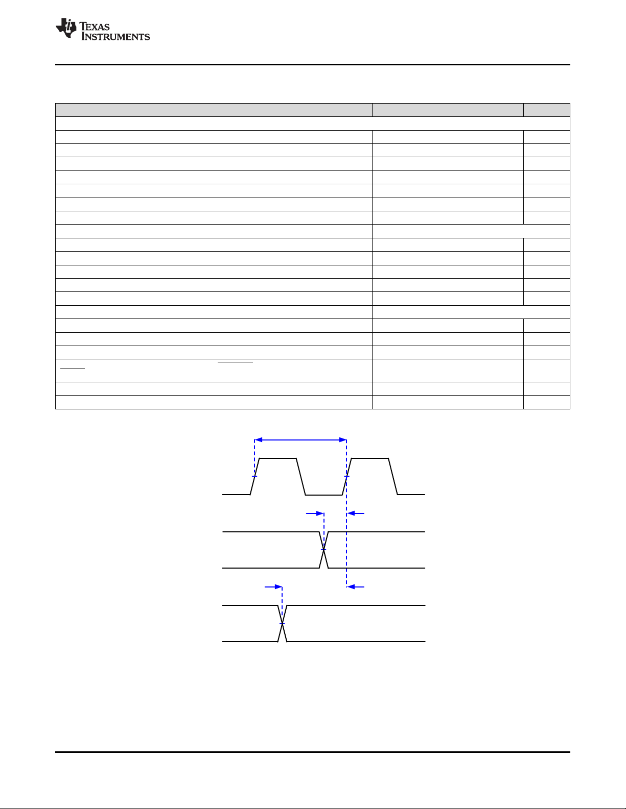
SERIAL CONTROL BUS TIMING PARAMETERS (See Figure 3 and Figure 4)
f
SCP_CLK
t
SCP_SKEW
t
SCP_DELAY
t
SCP_EN
t
r_SCP
t
fP
Clock Cycle DLCK_A or DCLKC_B 5 ns
Pulse Width DCLK_A or DCLK_B 2.5 ns
Setup Time, D_A[0:15] before DCLK_A .35 ns
Setup Time, D_B[0:15] before DCLK_B .35 ns
Hold Time, D_A[0:15] after DCLK_A .35 ns
Hold Time, D_B[0:15] after DCLK_B .35 ns
Channel B relative to Channel A –1.25 1.25 ns
Common Mode Voltage 1200 mV
LVDS Voltage 0 2000 mV
Rise Time (20% to 80%) 100 400 ps
Fall Time (80% to 20%) 100 400 ps
SCP Clock Frequency 50 500 kHz
Time between valid SCP_DI and rising edge of SCP_CLK –300 300 ns
Time between valid SCP_DO and rising edge of SCP_CLK 2600 ns
Time between falling edge of SCP_EN and the first rising edge of
SCP_CLK
30 ns
Rise time for SCP signals 200 ns
Fall time for SCP signals 200 ns
Figure 3. Serial Communications Bus Timing Parameters
Product Folder Links: DLP5500
Submit Documentation FeedbackCopyright © 2010–2019, Texas Instruments Incorporated
11
Page 12
V /2
CC
0 v
SCP_CLK,
SCP_DI,
SCP_EN
Input Controller V
CC
t
r_SCP
t
f_SCP
DLP5500
DLPS013G –APRIL 2010–REVISED JANUARY 2019
Figure 4. Serial Communications Bus Waveform Requirements
www.ti.com
12
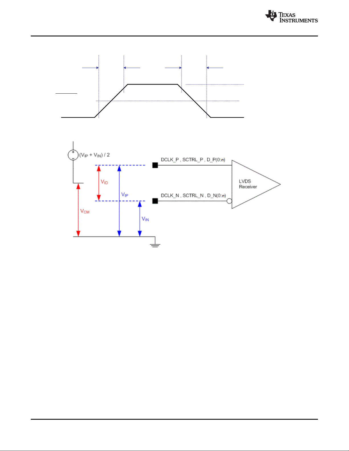
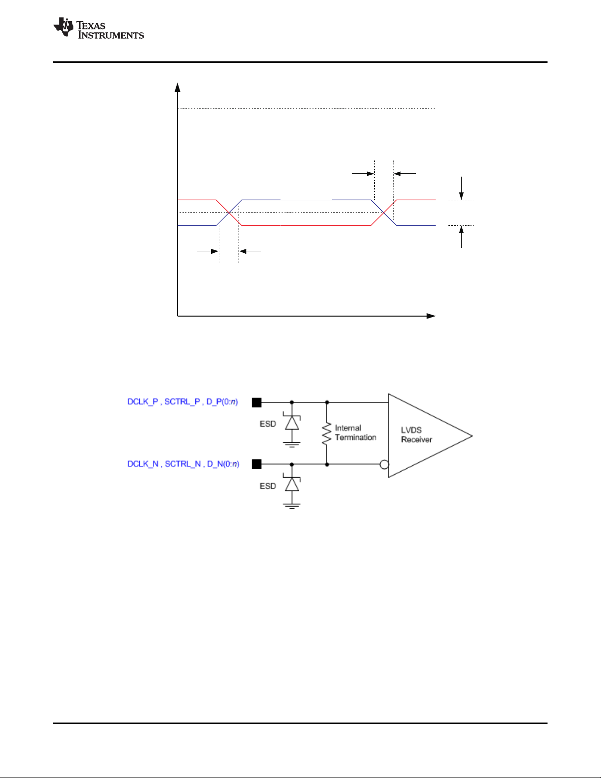
Refer to LVDS Interface section of the Recommended Operating Conditions.
Refer to Pin Configuration and Functions for list of LVDS pins.
Figure 5. LVDS Voltage Definitions (References)
Submit Documentation Feedback Copyright © 2010–2019, Texas Instruments Incorporated
Product Folder Links: DLP5500
Page 13
V
CM
V
LVDS
(v)
V
ID
Tr(20% - 80%)
Tf(20% - 80%)
Time
V
LVDSmax
V
LVDS min
V = V + |½V |
IDLVDSmax CM
V
LVDS
= VCM+/- | 1/2 VID|
V
LVDS min
= 0
www.ti.com
DLP5500
DLPS013G –APRIL 2010–REVISED JANUARY 2019
Not to scale.
Refer to LVDS Interface section of the Recommended Operating Conditions.
Figure 6. LVDS Waveform Requirements
Refer to LVDS Interface section of the Recommended Operating Conditions.
Refer to Pin Configuration and Functions for list of LVDS pins.
Figure 7. LVDS Equivalent Input Circuit
13
Submit Documentation FeedbackCopyright © 2010–2019, Texas Instruments Incorporated
Product Folder Links: DLP5500
Page 14
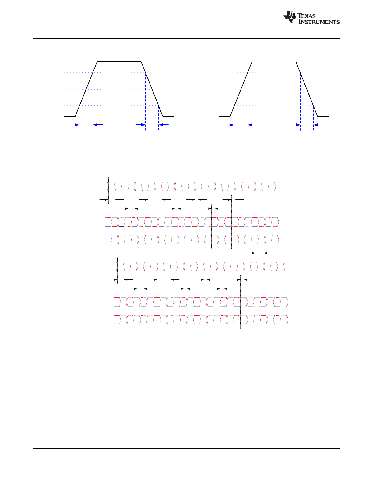
SCTRL_AN
SCTRL_AP
D_AN(15:0)
D_AP(15:0)
D_BN(15:0)
D_BP(15:0)
DCLK_BN
DCLK_BP
SCTRL_BN
SCTRL_BP
DCLK_AN
DCLK_AP
Tw
Tc
Tw
Th
Th
Ts
Ts
Tskew
Tw
Tc
Tw
Th
Th
Ts
Ts
0.0 * VCC
1.0 * VCC
t
f
t
r
1.0 * V
ID
0.0 * V
ID
V
CM
t
f
t
r
LVDS Interface SCP Interface
DLP5500
DLPS013G –APRIL 2010–REVISED JANUARY 2019
Not to scale.
Refer to the Timing Requirements.
Refer to Pin Configuration and Functions for list of LVDS pins and SCP pins.
www.ti.com
Figure 8. Rise Time and Fall Time
Figure 9. LVDS Timing Waveforms
14
Submit Documentation Feedback Copyright © 2010–2019, Texas Instruments Incorporated
Product Folder Links: DLP5500
Page 15

DLP5500
www.ti.com
DLPS013G –APRIL 2010–REVISED JANUARY 2019
8.8 System Mounting Interface Loads
PARAMETER MIN NOM MAX UNIT
Maximum system mounting interface
load to be applied to the:
Thermal Interface area Static load applied to the
thermal interface area,
See Figure 10
Electrical Interface area Static load applied to
each electrical interface
area no. 1 and no. 2,
See Figure 10
111 N
55 N
Figure 10. System Interface Loads
Product Folder Links: DLP5500
Submit Documentation FeedbackCopyright © 2010–2019, Texas Instruments Incorporated
15
Page 16

N ± 1
012
0
1
2
M ± 1
DMD Active Array
3
N ± 4
3
M ± 2
M ± 3
M ± 4
N ± 2
N ± 3
M x P
N x P
M x N Micromirrors
P
P
P
Border micromirrors omitted for clarity.
Not to scale.
P
Details omitted for clarity.
DLP5500
DLPS013G –APRIL 2010–REVISED JANUARY 2019
www.ti.com
8.9 Micromirror Array Physical Characteristics
Additional details are provided in the Mechanical, Packaging, and Orderable Information section at the end of this
document.
PARAMETER VALUE UNIT
M Number of active micromirror columns
N Number of active micromirror rows 768
P Micromirror pitch 10.8 µm
Micromirror active array width M × P 11.059 mm
Micromirror active array height N × P 8.294 mm
Micromirror active array border
(1) The structure and qualities of the border around the active array includes a band of partially functional micromirrors called the POM.
These micromirrors are structurally and/or electrically prevented from tilting toward the bright or ON state, but still require an electrical
bias to tilt toward OFF.
Pond of
Micromirror
(1)
(POM)
See Micromirror
Array Physical
Characteristics
1024
10 micromirrors /side
micromirrors
16
Submit Documentation Feedback Copyright © 2010–2019, Texas Instruments Incorporated
Refer to the Micromirror Array Physical Characteristics table for M, N, and P specifications.
Figure 11. Micromirror Array Physical Characteristics
Product Folder Links: DLP5500
Page 17

DLP5500
www.ti.com
DLPS013G –APRIL 2010–REVISED JANUARY 2019
8.10 Micromirror Array Optical Characteristics
TI assumes no responsibility for end-equipment optical performance. Achieving the desired end-equipment
optical performance involves making trade-off’s between numerous component and system design parameters.
See the Application Notes for additional details, considerations, and guidelines: DLP System Optics Application
Report (DLPA022).
PARAMETER CONDITIONS MIN NOM MAX UNIT
Micromirror tilt angle, a
Micromirror tilt angle variation, b
Micromirror Cross Over Time
Micromirror Switching Time
Non Operating micromirrors
Orientation of the micromirror axis-of-rotation
Micromirror array optical efficiency
Mirror metal specular reflectivity 420 - 700 89.4% nm
(1)(4) (6)(7)(8)
(9)
(10)
(11)
(12)
(13)(14)
DMD parked state
DMD landed state
See Figure 15 –1 1 degrees
Non-adjacent micromirrors 10
Adjacent micromirrors 0
See 44 45 46 degrees
420 - 700, with all micromirrors in the ON state 68% nm
(1)(2) (3)
, see Figure 15 0
(1)(4) (5)
, see Figure 15 12
degrees
16 22 µs
140 µs
micromirrors
(1) Measured relative to the plane formed by the overall micromirror array
(2) Parking the micromirror array returns all of the micromirrors to an essentially flat (0˚) state (as measured relative to the plane formed by
the overall micromirror array).
(3) When the micromirror array is parked, the tilt angle of each individual micromirror is uncontrolled.
(4) Additional variation exists between the micromirror array and the package datums, as shown in the section at the end of the document.
(5) When the micromirror array is landed, the tilt angle of each individual micromirror is dictated by the binary contents of the CMOS
memory cell associated with each individual micromirror. A binary value of 1 will result in a micromirror landing in an nominal angular
position of +12 degrees. A binary value of 0 will result in a micromirror landing in an nominal angular position of -12 degrees.
(6) Represents the landed tilt angle variation relative to the Nominal landed tilt angle.
(7) Represents the variation that can occur between any two individual micromirrors, located on the same device or located on different
devices.
(8) For some applications, it is critical to account for the micromirror tilt angle variation in the overall System Optical Design. With some
System Optical Designs, the micromirror tilt angle variations within a device may result in perceivable non-uniformities in the light field
reflected from the micromirror array. With some System Optical Designs, the micromirror tilt angle variation between devices may result
in colorimetry variations and/or system contrast variations.
(9) Micromirror Cross Over time is primarily a function of the natural response time of the micromirrors.
(10) Micromirror switching is controlled and coordinated by the DLPC200 (See DLPS014) and DLPA200 (See DLPS015). Nominal Switching
time depends on the system implementation and represents the time for the entire micromirror array to be refreshed.
(11) Non-operating micromirror is defined as a micromirror that is unable to transition nominally from the -12 degree position to +12 degree
or vice versa.
(12) Measured relative to the package datums B and C, shown in the Mechanical, Packaging, and Orderable Information section at the end
of this document.
(13) The minimum or maximum DMD optical efficiency observed in a specific application depends on numerous application-specific design
variables, such as but not limited to:
(a) Illumination wavelength, bandwidth or line-width, degree of coherence
(b) Illumination angle, plus angle tolerance
(c) Illumination and projection aperture size, and location in the system optical path
(d) IIlumination overfill of the DMD micromirror array
(e) Aberrations present in the illumination source and/or path
(f) Aberrations present in the projection path
The specified nominal DMD optical efficiency is based on the following use conditions:
(a) Visible illumination (420 nm – 700 nm)
(b) Input illumination optical axis oriented at 24° relative to the window normal
(c) Projection optical axis oriented at 0° relative to the window normal
(d) f/3.0 illumination aperture
(e) f/2.4 projection aperture
Based on these use conditions, the nominal DMD optical efficiency results from the following four components:
(a) Micromirror array fill factor: nominally 92%
(b) Micromirror array diffraction efficiency: nominally 86%
(c) Micromirror surface reflectivity: nominally 88%
(d) Window transmission: nominally 97% (single pass, through two surface transitions)
(14) Does not account for the effect of micromirror switching duty cycle, which is application dependant. Micromirror switching duty cycle
represents the percentage of time that the micromirror is actually reflecting light from the optical illumination path to the optical projection
path. This duty cycle depends on the illumination aperture size, the projection aperture size, and the micromirror array update rate.
Product Folder Links: DLP5500
Submit Documentation FeedbackCopyright © 2010–2019, Texas Instruments Incorporated
17
Page 18

N ± 1
012
0
1
2
M ± 1
3
N ± 4
3
M ± 2
M ± 3
M ± 4
N ± 2
N ± 3
45°
On-State
Tilt Direction
Off-State
Tilt Direction
Not To Scale
illumination
DLP5500
DLPS013G –APRIL 2010–REVISED JANUARY 2019
Refer to section Micromirror Array Physical Characteristics table for M, N, and P specifications.
Figure 12. Micromirror Landed Orientation and Tilt
www.ti.com
8.11 Window Characteristics
PARAMETER
Window material designation Corning Eagle XG
Window refractive index at wavelength 546.1 nm 1.5119
Window aperture See
Illumination overfill Refer to Illumination Overfill section
Window transmittance, single–pass
through both surfaces and glass
(1) See Window Characteristics and Optics for more information.
(2) For details regarding the size and location of the window aperture, see the package mechanical characteristics listed in the Mechanical
ICD in the Mechanical, Packaging, and Orderable Information section.
(3) See the TI application report Wavelength Transmittance Considerations for DLP®DMD Window DLPA031.
(1)
(2)
CONDITIONS MIN TYP MAX UNIT
At wavelength 405 nm. Applies to 0° and 24° AOI only. 95%
Minimum within the wavelength range 420 nm to 680 nm.
(3)
Applies to all angles 0° to 30° AOI.
Average over the wavelength range 420 nm to 680 nm.
Applies to all angles 30° to 45° AOI.
97%
97%
8.12 Chipset Component Usage Specification
The DLP5500 is a component of one or more DLP chipsets. Reliable function and operation of the DLP5500
requires that it be used in conjunction with the other components of the applicable DLP chipset, including those
components that contain or implement TI DMD control technology. TI DMD control technology is the TI
technology and devices for operating or controlling a DLP DMD.
18
Submit Documentation Feedback Copyright © 2010–2019, Texas Instruments Incorporated
Product Folder Links: DLP5500
Page 19

DLP5500
www.ti.com
DLPS013G –APRIL 2010–REVISED JANUARY 2019
9 Detailed Description
9.1 Overview
DLP5500 is a 0.55 inch diagonal spatial light modulator which consists of an array of highly reflective aluminum
micromirrors. Pixel array size and square grid pixel arrangement are shown in Figure 11.
The DMD is an electrical input, optical output micro-electrical-mechanical system (MEMS). The electrical
interface is Low Voltage Differential Signaling (LVDS), Double Data Rate (DDR).
DLP5500 DMD consists of a two-dimensional array of 1-bit CMOS memory cells. The array is organized in a grid
of M memory cell columns by N memory cell rows. Refer to the Functional Block Diagram.
The positive or negative deflection angle of the micromirrors can be individually controlled by changing the
address voltage of underlying CMOS addressing circuitry and micromirror reset signals (MBRST).
Each cell of the M × N memory array drives its true and complement (‘Q’ and ‘QB’) data to two electrodes
underlying one micromirror, one electrode on each side of the diagonal axis of rotation. Refer to Figure 15. The
micromirrors are electrically tied to the micromirror reset signals (MBRST) and the micromirror array is divided
into reset groups.
Electrostatic potentials between a micromirror and its memory data electrodes cause the micromirror to tilt
toward the illumination source in a DLP projection system or away from it, thus reflecting its incident light into or
out of an optical collection aperture. The positive (+) tilt angle state corresponds to an 'on' pixel, and the negative
(–) tilt angle state corresponds to an 'off' pixel.
Refer to Micromirror Array Optical Characteristics for the ± tilt angle specifications. Refer to the Pin Configuration
and Functions for more information on micromirror clocking pulse (reset) control.
Product Folder Links: DLP5500
Submit Documentation FeedbackCopyright © 2010–2019, Texas Instruments Incorporated
19
Page 20

DLP5500
DLPS013G –APRIL 2010–REVISED JANUARY 2019
9.2 Functional Block Diagram
www.ti.com
20
Figure 13. Functional Block Diagram
Submit Documentation Feedback Copyright © 2010–2019, Texas Instruments Incorporated
Product Folder Links: DLP5500
Page 21

DLP5500
www.ti.com
DLPS013G –APRIL 2010–REVISED JANUARY 2019
9.3 Feature Description
The DLP5500 device consists of 786,432 highly reflective, digitally switchable, micrometer-sized mirrors
(micromirrors) organized in a two-dimensional orthogonal pixel array. Refer to Figure 11 and Figure 14.
Each aluminum micromirror is switchable between two discrete angular positions, –a and +a. The angular
positions are measured relative to the micromirror array plane, which is parallel to the silicon substrate. Refer to
Micromirror Array Optical Characteristics and Figure 15.
The parked position of the micromirror is not a latched position and is therefore not necessarily perfectly parallel
to the array plane. Individual micromirror flat state angular positions may vary. Tilt direction of the micromirror is
perpendicular to the hinge-axis. The on-state landed position is directed toward the left-top edge of the package,
as shown in Figure 14.
Each individual micromirror is positioned over a corresponding CMOS memory cell. The angular position of a
specific micromirror is determined by the binary state (logic 0 or 1) of the corresponding CMOS memory cell
contents, after the mirror clocking pulse is applied. The angular position (–a and +a) of the individual
micromirrors changes synchronously with a micromirror clocking pulse, rather than being coincident with the
CMOS memory cell data update.
Writing logic 1 into a memory cell followed by a mirror clocking pulse results in the corresponding micromirror
switching to the +a position. Writing logic 0 into a memory cell followed by a mirror clocking pulse results in the
corresponding micromirror switching to the – a position.
Updating the angular position of the micromirror array consists of two steps. First, update the contents of the
CMOS memory. Second, apply a micromirror clocking pulse (reset) to all or a portion of the micromirror array
(depending upon the configuration of the system). Micromirror reset pulses are generated externally by the
DLPC200 controller in conjunction with the DLPA200 analog driver, with application of the pulses being
coordinated by the DLPC200 controller.
For more information, see the TI application report DLPA008, DMD101: Introduction to Digital Micromirror Device
(DMD) Technology.
Product Folder Links: DLP5500
Submit Documentation FeedbackCopyright © 2010–2019, Texas Instruments Incorporated
21
Page 22

DMD
Micromirror
Array
0
N±1
0
M±1
Active Micromirror Array
(Border micromirrors eliminated for clarity)
P (um)
Micromirror Pitch
Micromirror Hinge-Axis Orientation
³2Q-6WDWH´
Tilt Direction
³2II-6WDWH´
Tilt Direction
45°
P (um)
P (um)
P (um)
Incident
Illumination
Package Pin
A1 Corner
Details Omitted For Clarity.
Not To Scale.
DLP5500
DLPS013G –APRIL 2010–REVISED JANUARY 2019
Feature Description (continued)
www.ti.com
22
Refer to Figure 11 and Figure 12.
Figure 14. Micromirror Array, Pitch, Hinge Axis Orientation
Submit Documentation Feedback Copyright © 2010–2019, Texas Instruments Incorporated
Product Folder Links: DLP5500
Page 23

DMD
For Reference
Flat-State
( ³SDUNHG´)
Micromirror Position
³2II-6WDWH´
Micromirror
³2Q-6WDWH´
Micromirror
Silicon SubstrateSilicon Substrate
a ± b
-a ± b
Two
³2Q-6WDWH´
Micromirrors
Two
³2II-6WDWH´
Micromirrors
Incident
Illumination-Light Path
Incident
Illumination
-
Light Path
Projected-Light
Path
Off
-
State
-
Light
Path
Package Pin
A1 Corner
Details Omitted For Clarity.
Not To Scale.
Incident
Illumination
Incident
Illumination-Light Path
www.ti.com
Feature Description (continued)
DLP5500
DLPS013G –APRIL 2010–REVISED JANUARY 2019
Micromirror States: On, Off, Flat
Figure 15. Micromirror States: On, Off, Flat
Product Folder Links: DLP5500
Submit Documentation FeedbackCopyright © 2010–2019, Texas Instruments Incorporated
23
Page 24

DLP5500
DLPS013G –APRIL 2010–REVISED JANUARY 2019
www.ti.com
9.4 Device Functional Modes
DMD functional modes are controlled by the DLPC200 digital display controller. See the DLPC200 data sheet
listed in Related Documentation. Contact a TI applications engineer for more information.
The DLPC200 provides two basic functional mode types to control the DLP5500 DMD: video and structured light.
9.4.1 Video Modes
The controller accepts RGB-8-8-8 input to port 1 or port 2 through a selectable MUX. XGA video information is
displayed on the DMD at 6 to 60 fps.
An internal pattern generator can generate RGB-8-8-8 video patterns into an internal selectable MUX for
verification and debug purposes.
9.4.2 Structured Light Modes
The DLPC200 provides two structured light modes: static image buffer and real-time structured light.
9.4.2.1 Static Image Buffer Mode
Image data can be loaded into parallel flash memory to load to DDR2 memory at startup to be displayed, or can
be loaded over USB or the SPI port directly to DDR2 memory to be displayed. Binary (1-bit) or grayscale (8-bit)
patterns can be displayed. The memory will hold 960 binary patterns or 120 grayscale patterns.
Binary (1-bit) patterns can be displayed at up to 5000 binary patterns per second. These patterns assume a
constant illumination and do not depend on illumination modulation
Grayscale (8-bit) patterns assume illumination modulation in order to achieve higher pattern rates. When the
pattern rate requires that the lower significant bit(s) be shorter than the rate that the DMD can be switched, these
bits will require the source to be modulated to achieve the shorter time required. The trade-off is dark time during
these bits. At the maximum 500 Hz grayscale pattern rate, the dark time approaches 75%.
9.4.2.2 Real Time Structured Light Mode
RGB-8-8-8 60 fps data can be input into port 1 or port 2 and reinterpreted as up to 24 binary (1-bit) patterns or
three grayscale (8-bit) patterns. The specified number of patterns is displayed equally during the exposure time
specified. Any unused RGB-8-8-8 data in the video frame must be filled with data, usually 0s.
For example, during one video frame (16.67 ms), 12 binary patterns of the 24 RGB bits are requested to be
displayed during half of the video frame time (exposure time = 8.33 ms). Each of the eight red bits and the four
most significant green bits are displayed as a binary pattern for 694 µs each. The remaining bits are ignored and
the remaining 8.33 ms of the frame will be dark.
9.5 Window Characteristics and Optics
NOTE
TI assumes no responsibility for image quality artifacts or DMD failures caused by optical
system operating conditions exceeding limits described previously.
9.5.1 Optical Interface and System Image Quality
TI assumes no responsibility for end-equipment optical performance. Achieving the desired end-equipment
optical performance involves making trade-offs between numerous component and system design parameters.
Optimizing system optical performance and image quality strongly relate to optical system design parameter
trades. Although it is not possible to anticipate every conceivable application, projector image quality and optical
performance is contingent on compliance to the optical system operating conditions described in the following
sections.
24
Submit Documentation Feedback Copyright © 2010–2019, Texas Instruments Incorporated
Product Folder Links: DLP5500
Page 25

DLP5500
www.ti.com
DLPS013G –APRIL 2010–REVISED JANUARY 2019
Window Characteristics and Optics (continued)
9.5.2 Numerical Aperture and Stray Light Control
The angle defined by the numerical aperture of the illumination and projection optics at the DMD optical area
should be the same. This angle should not exceed the nominal device mirror tilt angle unless appropriate
apertures are added in the illumination and/or projection pupils to block out flat-state and stray light from the
projection lens. The mirror tilt angle defines DMD capability to separate the "ON" optical path from any other light
path, including undesirable flat-state specular reflections from the DMD window, DMD border structures, or other
system surfaces near the DMD such as prism or lens surfaces. If the numerical aperture exceeds the mirror tilt
angle, or if the projection numerical aperture angle is more than two degrees larger than the illumination
numerical aperture angle, objectionable artifacts in the display’s border and/or active area could occur.
9.5.3 Pupil Match
TI’s optical and image quality specifications assume that the exit pupil of the illumination optics is nominally
centered within 2° (two degrees) of the entrance pupil of the projection optics. Misalignment of pupils can create
objectionable artifacts in the display’s border and/or active area, which may require additional system apertures
to control, especially if the numerical aperture of the system exceeds the pixel tilt angle.
9.5.4 Illumination Overfill
The active area of the device is surrounded by an aperture on the inside DMD window surface that masks
structures of the DMD device assembly from normal view. The aperture is sized to anticipate several optical
operating conditions. Overfill light illuminating the window aperture can create artifacts from the edge of the
window aperture opening and other surface anomalies that may be visible on the screen. The illumination optical
system should be designed to limit light flux incident anywhere on the window aperture from exceeding
approximately 10% of the average flux level in the active area. Depending on the particular system’s optical
architecture, overfill light may have to be further reduced below the suggested 10% level in order to be
acceptable.
9.6 Micromirror Array Temperature Calculation
Achieving optimal DMD performance requires proper management of the maximum DMD case temperature, the
maximum temperature of any individual micromirror in the active array, the maximum temperature of the window
aperture, and the temperature gradient between case temperature and the predicted micromirror array
temperature. (see Figure 16).
Refer to the Recommended Operating Conditions for applicable temperature limits.
9.6.1 Package Thermal Resistance
The DMD is designed to conduct absorbed and dissipated heat to the back of the Series 450 package where it
can be removed by an appropriate heat sink. The heat sink and cooling system must be capable of maintaining
the package within the specified operational temperatures, refer to Figure 16. The total heat load on the DMD is
typically driven by the incident light absorbed by the active area; although other contributions include light energy
absorbed by the window aperture and electrical power dissipation of the array.
9.6.2 Case Temperature
The temperature of the DMD case can be measured directly. For consistency, Thermal Test Point locations TP1
- TP5 are defined, as shown in Figure 16.
Product Folder Links: DLP5500
Submit Documentation FeedbackCopyright © 2010–2019, Texas Instruments Incorporated
25
Page 26

DLP5500
DLPS013G –APRIL 2010–REVISED JANUARY 2019
Micromirror Array Temperature Calculation (continued)
www.ti.com
Figure 16. Thermal Test Point Location
9.6.3 Micromirror Array Temperature Calculation for Uniform Illumination
Micromirror array temperature cannot be measured directly; therefore it must be computed analytically from
measurement points (Figure 16), the package thermal resistance, the electrical power, and the illumination heat
load. The relationship between micromirror array temperature and the case temperature are provided by
Equation 1 and Equation 2:
T
Q
Array
Array
= T
= Q
Ceramic
ELE
+ Q
+ (Q
ILL
Array
x R
Array-To-Ceramic
) (1)
Where the following elements are defined as:
• T
• T
• Q
• R
• Q
• Q
= computed micromirror array temperature (°C)
Array
= Ceramic temperature (°C) (TC2 Location Figure 16)
Ceramic
= Total DMD array power (electrical + absorbed) (measured in Watts)
Array
Array-To-Ceramic
= thermal resistance of DMD package from array to TC2 (°C/Watt) (see Package Thermal
Resistance)
= Nominal electrical power (Watts)
ELE
= Absorbed illumination energy (Watts) (2)
ILL
An example calculation is provided below based on a traditional DLP Video projection system. The electrical
power dissipation of the DMD is variable and depends on the voltages, data rates, and operating frequencies.
The nominal electrical power dissipation to be used in the calculation is 2.0 Watts. Thus, Q
= 2.0 Watts. The
ELE
absorbed power from the illumination source is variable and depends on the operating state of the mirrors and
the intensity of the light source. It's based on modeling and measured data from DLP projection system.
Q
= C
L2W
x SL
ILL
Where:
• C
• SL = Screen Lumens nominally measured to be 2000 lumens
• Qarray = 2.0 + (0.00274 x 2000) = 7.48 watts, Estimated total power on micromirror Array
• T
• T
is a Lumens to Watts constant, and can be estimated at 0.00274 Watt/Lumen
L2W
= 55°C, assumed system measurement
Ceramic
(micromirror active array temperature) = 55°C + (7.48 watts x 0.6 °C/watt) = 59.5°C (3)
Array
26
Submit Documentation Feedback Copyright © 2010–2019, Texas Instruments Incorporated
Product Folder Links: DLP5500
Page 27

DLP5500
www.ti.com
DLPS013G –APRIL 2010–REVISED JANUARY 2019
Micromirror Array Temperature Calculation (continued)
For additional explanation of DMD Mechanical and Thermal calculations and considerations please refer to DLP
Series-450 DMD and System Mounting Concepts (DLPA015).
9.7 Micromirror Landed-on/Landed-Off Duty Cycle
9.7.1 Definition of Micromirror Landed-On/Landed-Off Duty Cycle
The micromirror landed-on/landed-off duty cycle (landed duty cycle) denotes the amount of time (as a
percentage) that an individual micromirror is landed in the On–state versus the amount of time the same
micromirror is landed in the Off–state.
As an example, a landed duty cycle of 100/0 indicates that the referenced pixel is in the On-state 100% of the
time (and in the Off-state 0% of the time); whereas 0/100 would indicate that the pixel is in the Off-state 100% of
the time. Likewise, 50/50 indicates that the pixel is On 50% of the time and Off 50% of the time.
Note that when assessing landed duty cycle, the time spent switching from one state (ON or OFF) to the other
state (OFF or ON) is considered negligible and is thus ignored.
Since a micromirror can only be landed in one state or the other (On or Off), the two numbers (percentages)
always add to 100.
9.7.2 Landed Duty Cycle and Useful Life of the DMD
Knowing the long-term average landed duty cycle (of the end product or application) is important because
subjecting all (or a portion) of the DMD’s micromirror array (also called the active array) to an asymmetric landed
duty cycle for a prolonged period of time can reduce the DMD’s usable life.
Note that it is the symmetry/asymmetry of the landed duty cycle that is of relevance. The symmetry of the landed
duty cycle is determined by how close the two numbers (percentages) are to being equal. For example, a landed
duty cycle of 50/50 is perfectly symmetrical whereas a landed duty cycle of 100/0 or 0/100 is perfectly
asymmetrical.
9.7.3 Landed Duty Cycle and Operational DMD Temperature
Operational DMD Temperature and Landed Duty Cycle interact to affect the DMD’s usable life, and this
interaction can be exploited to reduce the impact that an asymmetrical Landed Duty Cycle has on the DMD’s
usable life. This is quantified in the de-rating curve shown in Figure 1. The importance of this curve is that:
• All points along this curve represent the same usable life.
• All points above this curve represent lower usable life (and the further away from the curve, the lower the
usable life).
• All points below this curve represent higher usable life (and the further away from the curve, the higher the
usable life).
In practice, this curve specifies the Maximum Operating DMD Temperature that the DMD should be operated at
for a give long-term average Landed Duty Cycle.
9.7.4 Estimating the Long-Term Average Landed Duty Cycle of a Product or Application
During a given period of time, the Landed Duty Cycle of a given pixel follows from the image content being
displayed by that pixel.
For example, in the simplest case, when displaying pure-white on a given pixel for a given time period, that pixel
will experience a 100/0 Landed Duty Cycle during that time period. Likewise, when displaying pure-black, the
pixel will experience a 0/100 Landed Duty Cycle.
Between the two extremes (ignoring for the moment color and any image processing that may be applied to an
incoming image), the Landed Duty Cycle tracks one-to-one with the gray scale value, as shown in Table 1.
Product Folder Links: DLP5500
Submit Documentation FeedbackCopyright © 2010–2019, Texas Instruments Incorporated
27
Page 28

DLP5500
DLPS013G –APRIL 2010–REVISED JANUARY 2019
www.ti.com
Table 1. Grayscale Value and Landed Duty Cycle
GRAYSCALE VALUE LANDED DUTY CYCLE
0% 0/100
10% 10/90
20% 20/80
30% 30/70
40% 40/60
50% 50/50
60% 60/40
70% 70/30
80% 80/20
90% 90/10
100% 100/0
Accounting for color rendition (but still ignoring image processing) requires knowing both the color intensity (from
0% to 100%) for each constituent primary color (red, green, and/or blue) for the given pixel as well as the color
cycle time for each primary color, where “color cycle time” is the total percentage of the frame time that a given
primary must be displayed in order to achieve the desired white point.
During a given period of time, the landed duty cycle of a given pixel can be calculated as follows:
Landed Duty Cycle = (Red_Cycle_% × Red_Scale_Value) + (Green_Cycle_% × Green_Scale_Value) + (Blue_Cycle_%
× Blue_Scale_Value)
where
• Red_Cycle_%, Green_Cycle_%, and Blue_Cycle_%, represent the percentage of the frame time that Red,
Green, and Blue are displayed (respectively) to achieve the desired white point. (4)
For example, assume that the red, green and blue color cycle times are 50%, 20%, and 30% respectively (in
order to achieve the desired white point), then the Landed Duty Cycle for various combinations of red, green,
blue color intensities would be as shown in Table 2.
Table 2. Example Landed Duty Cycle for Full-Color
Red Cycle Percentage
50%
Red Scale Value Green Scale Value Blue Scale Value
0% 0% 0% 0/100
100% 0% 0% 50/50
0% 100% 0% 20/80
0% 0% 100% 30/70
12% 0% 0% 6/94
0% 35% 0% 7/93
0% 0% 60% 18/82
100% 100% 0% 70/30
0% 100% 100% 50/50
100% 0% 100% 80/20
12% 35% 0% 13/87
0% 35% 60% 25/75
12% 0% 60% 24/76
100% 100% 100% 100/0
Green Cycle Percentage
20%
Blue Cycle Percentage
30%
Landed Duty Cycle
28
Submit Documentation Feedback Copyright © 2010–2019, Texas Instruments Incorporated
Product Folder Links: DLP5500
Page 29

DLP5500
www.ti.com
DLPS013G –APRIL 2010–REVISED JANUARY 2019
10 Application and Implementation
NOTE
Information in the following applications sections is not part of the TI component
specification, and TI does not warrant its accuracy or completeness. TI’s customers are
responsible for determining suitability of components for their purposes. Customers should
validate and test their design implementation to confirm system functionality.
10.1 Application Information
The DLP5500 (0.55-inch XGA DMD) is controlled by the DLPC200 contoller in conjunction with the DLPA200
driver. This combination can be used for a number of applications from 3D printers to microscopes.
The most common application is for 3D structured light measurement applications. In this application, patterns
(binary, grayscale, or even full color) are projected onto the target and the distortion of the patterns are recorded
by an imaging device to extract 3D (x, y, z) surface information.
Product Folder Links: DLP5500
Submit Documentation FeedbackCopyright © 2010–2019, Texas Instruments Incorporated
29
Page 30

Expansion Port
Connector
DLPA200 Control Interface
Micromirror
Resets
Micromirror Data Interface
Micromirror Control Interface
RED ENABLE
GREEN ENABLE
BLUE ENABLE
INFRARED ENABLE
LED Lit Status
LED SPI Interface
Port 2 DATA( 23:0 )
Port 2 VSYNC
Port 2 HSYNC
Port 2 Data Valid
Port 2 Clock
Port 1 DATA( 23:0 )
Port 1 VSYNC
Port 1 HSYNC
Port 1 Data Valid
Port 1 Clock
I2C Interface
Port 1 Interface
Port 2 Interface
DMD Interface
Illumination Interface
DLPA200 Interface
SYNC OUT 1
SYNC OUT 2
SYNC OUT 3
User SYNC Interface
Illumination
Optics
Projection
Optics
Configuration Interface
RESET
SRAM_CE
FLASH_SRAM_OE
FLASH_SRAM_WE
FLASH_SRAM_RST
FLASH_CE
SRAM_LB, SRAM_UB
USB Interface
SDRAM Interface
User Flash / SRAM Interface
Port 2 SPI Interface
HDMI
DLPR200USB PROM
DLPR200USB
DLPR200F PROM
DLPR200F
DLP5500
DLPS013G –APRIL 2010–REVISED JANUARY 2019
www.ti.com
10.2 Typical Application
A schematic is shown in Figure 17 for projecting RGB and IR structured light patterns onto a measurement
target. Typically, an imaging device is triggered through one of the three syncs to record the data as each pattern
is displayed.
30
Figure 17. Typical RGB + IR Structured Light Application
Submit Documentation Feedback Copyright © 2010–2019, Texas Instruments Incorporated
Product Folder Links: DLP5500
Page 31

DLP5500
www.ti.com
DLPS013G –APRIL 2010–REVISED JANUARY 2019
Typical Application (continued)
10.2.1 Design Requirements
All applications using the DLP 0.55-inch XGA chipset require the DLPC200 controller, the DLPA200 driver, and
the DLP5500 DMD for correct operation. The system also requires user supplied SRAM and a configuration
PROM programmed with the DLPR200F program file and a 50-MHz oscillator is for operation. For further details,
refer to the DLPC200 controller data sheet (DLPS014) and the DLPA200 analog driver data sheet (DLPS015).
10.2.2 Detailed Design Procedure
10.2.2.1 DLP5500 System Interface
Images are displayed on the DLP5500 via the DLPC200 controller and the DLPA200 driver. The DLP5500
interface consists of a 200-MHz (nominal) half-bus DDR input-only interface with LVDS signaling. The serial
communications port (SCP), 125-kHz nominal, is used by the DLPC200 to read or write control data to both the
DLP5500 and the DLPA200. The following listed signals support data transfer to the DLP5500 and DLPA200.
• DMD, 200 MHz
– DMD_CLK_AP, DMD_CLK_AN – DMD clock for A
– DMD_CLK_BP, DMD_CLK_BN – DMD clock for B
– DMD_DAT_AP, DMD_DAT_AN(1, 3, 5, 7, 9, 11, 13, 15) – Data bus A (odd-numbered pins are used for
half-bus)
– DMD_DAT_BP, DMD_DAT_BN(1, 3, 5, 7, 9, 11, 13, 15) – Data bus B (odd-numbered pins are used for
half-bus)
– DMD_SCRTL_AP, DMD_SCRTL_AN – S-control for A
– DMD_SCRTL_BP, DMD_SCRTL_BN – S-control for B
• DLPA200, 125 kHz
– SCP_DMD_RST_CLK – SCP clock
– SCP_DMD_EN – Enable DMD communication
– SCP_RST_EN – Enable DLPA200 communication
– SCP_DMD_RST_DI – Input data
– SCP_DMD_RST_DO – Output data
Product Folder Links: DLP5500
Submit Documentation FeedbackCopyright © 2010–2019, Texas Instruments Incorporated
31
Page 32

DLP5500
DLPS013G –APRIL 2010–REVISED JANUARY 2019
www.ti.com
11 Power Supply Recommendations
11.1 DMD Power-Up and Power-Down Procedures
The DLP5500 power-up and power-down procedures are defined by the DLPC200 data sheet (DLPS012) and
the 0.55 XGA Chipset data sheet (DLPZ004). These procedures must be followed to ensure reliable operation of
the device.
CAUTION
Failure to adhere to the prescribed power-up and power-down procedures may affect
device reliability.
12 Layout
12.1 Layout Guidelines
The DLP5500 is part of a chipset that is controlled by the DLPC200 in conjunction with the DLPA200. These
guidelines are targeted at designing a PCB board with these components.
12.1.1 Impedance Requirements
Signals should be routed to have a matched impedance of 50 Ω ±10% except for LVDS differential pairs
(DMD_DAT_Xnn, DMD_DCKL_Xn, and DMD_SCTRL_Xn) and DDR2 differential clock pairs (MEM_CLK_nn),
which should be matched to 100 Ω ±10% across each pair.
12.1.2 PCB Signal Routing
When designing a PCB board for the DLP5500 controlled by the DLPC200 in conjunction with the DLPA200, the
following are recommended:
Signal trace corners should be no sharper than 45°. Adjacent signal layers should have the predominate traces
routed orthogonal to each other. TI recommends that critical signals be hand routed in the following order: DDR2
Memory, DMD (LVDS signals), then DLPA200 signals.
TI does not recommend signal routing on power or ground planes.
TI does not recommend ground plane slots.
High speed signal traces should not cross over slots in adjacent power and/or ground planes.
Table 3. LVDS Trace Constraints
Signal Constraints
P-to-N data, clock, and SCTRL: <10 mils (0.25 mm); Pair-to-pair <10 mils (0.25 mm); Bundle-to-bundle
LVDS (DMD_DAT_xnn,
DMD_DCKL_xn, and
DMD_SCTRL_xn)
<2000 mils (50 mm, for example DMD_DAT_Ann to DMD_DAT_Bnn).
All matching should include internal trace lengths. See Pin Configuration and Functions for internal
package trace lengths.
Trace width: 4 mil (0.1 mm)
Trace spacing: In ball field – 4 mil (0.11 mm); PCB etch – 14 mil (0.36 mm)
Maximum recommended trace length <6 inches (150 mm)
Table 4. Power and Mirror Clocking Pulse Trace Widths and Spacing
Signal Name
GND Maximize 5 mil (0.13 mm) Maximize trace width to connecting pin as a minimum
VCC, VCC2 20 mil (0.51 mm) 10 mil (0.25 mm)
MBRST[15:0] 10 mil (0.25 mm) 10 mil (0.25 mm)
Minimum Trace
Width
Minimum Trace
Spacing
Layout Requirements
32
Submit Documentation Feedback Copyright © 2010–2019, Texas Instruments Incorporated
Product Folder Links: DLP5500
Page 33

DLP5500
www.ti.com
DLPS013G –APRIL 2010–REVISED JANUARY 2019
12.1.3 Fiducials
Fiducials for automatic component insertion should be 0.05-inch copper with a 0.1-inch cutout (antipad). Fiducials
for optical auto insertion are placed on three corners of both sides of the PCB.
12.2 Layout Example
For LVDS (and other differential signal) pairs and groups, it is important to match trace lengths. In the area of the
dashed lines, Figure 18 shows correct matching of signal pair lengths with serpentine sections to maintain the
correct impedance.
Figure 18. Mitering LVDS Traces to Match Lengths
Product Folder Links: DLP5500
Submit Documentation FeedbackCopyright © 2010–2019, Texas Instruments Incorporated
33
Page 34

G H X X X X X L L L L L L M
* 1 0 7 6 X X X X X X
Y Y Y Y Y Y Y
2-Dimensional Matrix Code
(DLP5500 Device Descriptor
and Serial No.)
Part 2 of Serial Number
(7 characters)
TI Internal Numbering
DLP5500
Device Descriptor
Part 1 of Serial Number
(7 characters)
YYYYYYY
1076-6438B
GHXXXXX LLLLLLM
DLP5500
DLPS013G –APRIL 2010–REVISED JANUARY 2019
13 Device and Documentation Support
13.1 Device Support
13.1.1 Device Nomenclature
The device marking consists of the fields shown in Figure 19.
www.ti.com
Figure 19. DMD Marking (Device Top View)
13.2 Documentation Support
13.2.1 Related Documentation
The following documents contain additional information related to the use of the DLP5500 device:
• DLP 0.55 XGA Chip-Set data sheet DLPZ004
• DLPC200 Digital Controller data sheet DLPS014
• DLPA200 DMD Analog Reset Driver DLPS015
• DLP Series-450 DMD and System Mounting Concepts DLPA015
• DLPC200 API Reference Manual DLPA024
• DLPC200 API Programmer's Guide DLPA014
• s4xx DMD Cleaning Application Note DLPA025
• s4xx DMD Handling Application Note DLPA019
13.3 Related Documentation
The table below lists quick access links. Categories include technical documents, support and community
resources, tools and software, and quick access to sample or buy.
Related Links
PARTS PRODUCT FOLDER SAMPLE & BUY
DLPA200 Click here Click here Click here Click here Click here
DLPC200 Click here Click here Click here Click here Click here
TECHNICAL
DOCUMENTS
TOOLS &
SOFTWARE
SUPPORT &
COMMUNITY
13.4 Community Resources
The following links connect to TI community resources. Linked contents are provided "AS IS" by the respective
contributors. They do not constitute TI specifications and do not necessarily reflect TI's views; see TI's Terms of
Use.
TI E2E™ Online Community TI's Engineer-to-Engineer (E2E) Community. Created to foster collaboration
34
Submit Documentation Feedback Copyright © 2010–2019, Texas Instruments Incorporated
Product Folder Links: DLP5500
Page 35

DLP5500
www.ti.com
DLPS013G –APRIL 2010–REVISED JANUARY 2019
Community Resources (continued)
among engineers. At e2e.ti.com, you can ask questions, share knowledge, explore ideas and help
solve problems with fellow engineers.
Design Support TI's Design Support Quickly find helpful E2E forums along with design support tools and
contact information for technical support.
13.5 Trademarks
E2E is a trademark of Texas Instruments.
DLP is a registered trademark of Texas Instruments.
All other trademarks are the property of their respective owners.
13.6 Electrostatic Discharge Caution
These devices have limited built-in ESD protection. The leads should be shorted together or the device placed in conductive foam
during storage or handling to prevent electrostatic damage to the MOS gates.
13.7 Glossary
SLYZ022 — TI Glossary.
This glossary lists and explains terms, acronyms, and definitions.
14 Mechanical, Packaging, and Orderable Information
The following pages include mechanical, packaging, and orderable information. This information is the most
current data available for the designated devices. This data is subject to change without notice and revision of
this document. For browser-based versions of this data sheet, refer to the left-hand navigation.
Product Folder Links: DLP5500
Submit Documentation FeedbackCopyright © 2010–2019, Texas Instruments Incorporated
35
Page 36

PACKAGE OPTION ADDENDUM
www.ti.com
PACKAGING INFORMATION
Orderable Device Status
DLP5500BFYA ACTIVE CPGA FYA 149 5 RoHS & Green NI-PD-AU N / A for Pkg Type
DLPA200PFP ACTIVE HTQFP PFP 80 5 TBD Call TI Call TI
DLPC200ZEW ACTIVE BGA ZEW 780 5 TBD Call TI Call TI
(1)
The marketing status values are defined as follows:
ACTIVE: Product device recommended for new designs.
LIFEBUY: TI has announced that the device will be discontinued, and a lifetime-buy period is in effect.
NRND: Not recommended for new designs. Device is in production to support existing customers, but TI does not recommend using this part in a new design.
PREVIEW: Device has been announced but is not in production. Samples may or may not be available.
OBSOLETE: TI has discontinued the production of the device.
Package Type Package
(1)
Drawing
Pins Package
Qty
Eco Plan
(2)
Lead finish/
Ball material
(6)
MSL Peak Temp
(3)
Op Temp (°C) Device Marking
(4/5)
(2)
RoHS: TI defines "RoHS" to mean semiconductor products that are compliant with the current EU RoHS requirements for all 10 RoHS substances, including the requirement that RoHS substance
do not exceed 0.1% by weight in homogeneous materials. Where designed to be soldered at high temperatures, "RoHS" products are suitable for use in specified lead-free processes. TI may
reference these types of products as "Pb-Free".
RoHS Exempt: TI defines "RoHS Exempt" to mean products that contain lead but are compliant with EU RoHS pursuant to a specific EU RoHS exemption.
Green: TI defines "Green" to mean the content of Chlorine (Cl) and Bromine (Br) based flame retardants meet JS709B low halogen requirements of <=1000ppm threshold. Antimony trioxide based
flame retardants must also meet the <=1000ppm threshold requirement.
(3)
MSL, Peak Temp. - The Moisture Sensitivity Level rating according to the JEDEC industry standard classifications, and peak solder temperature.
(4)
There may be additional marking, which relates to the logo, the lot trace code information, or the environmental category on the device.
(5)
Multiple Device Markings will be inside parentheses. Only one Device Marking contained in parentheses and separated by a "~" will appear on a device. If a line is indented then it is a continuation
of the previous line and the two combined represent the entire Device Marking for that device.
(6)
Lead finish/Ball material - Orderable Devices may have multiple material finish options. Finish options are separated by a vertical ruled line. Lead finish/Ball material values may wrap to two
lines if the finish value exceeds the maximum column width.
Important Information and Disclaimer:The information provided on this page represents TI's knowledge and belief as of the date that it is provided. TI bases its knowledge and belief on information
provided by third parties, and makes no representation or warranty as to the accuracy of such information. Efforts are underway to better integrate information from third parties. TI has taken and
continues to take reasonable steps to provide representative and accurate information but may not have conducted destructive testing or chemical analysis on incoming materials and chemicals.
TI and TI suppliers consider certain information to be proprietary, and thus CAS numbers and other limited information may not be available for release.
9-Sep-2020
Samples
Addendum-Page 1
Page 37

PACKAGE OPTION ADDENDUM
www.ti.com
In no event shall TI's liability arising out of such information exceed the total purchase price of the TI part(s) at issue in this document sold by TI to Customer on an annual basis.
9-Sep-2020
Addendum-Page 2
Page 38

Page 39

Page 40

Page 41

Page 42

Page 43

Page 44

Page 45

www.ti.com
Page 46

IMPORTANT NOTICE AND DISCLAIMER
TI PROVIDES TECHNICAL AND RELIABILITY DATA (INCLUDING DATASHEETS), DESIGN RESOURCES (INCLUDING REFERENCE
DESIGNS), APPLICATION OR OTHER DESIGN ADVICE, WEB TOOLS, SAFETY INFORMATION, AND OTHER RESOURCES “AS IS”
AND WITH ALL FAULTS, AND DISCLAIMS ALL WARRANTIES, EXPRESS AND IMPLIED, INCLUDING WITHOUT LIMITATION ANY
IMPLIED WARRANTIES OF MERCHANTABILITY, FITNESS FOR A PARTICULAR PURPOSE OR NON-INFRINGEMENT OF THIRD
PARTY INTELLECTUAL PROPERTY RIGHTS.
These resources are intended for skilled developers designing with TI products. You are solely responsible for (1) selecting the appropriate
TI products for your application, (2) designing, validating and testing your application, and (3) ensuring your application meets applicable
standards, and any other safety, security, or other requirements. These resources are subject to change without notice. TI grants you
permission to use these resources only for development of an application that uses the TI products described in the resource. Other
reproduction and display of these resources is prohibited. No license is granted to any other TI intellectual property right or to any third
party intellectual property right. TI disclaims responsibility for, and you will fully indemnify TI and its representatives against, any claims,
damages, costs, losses, and liabilities arising out of your use of these resources.
TI’s products are provided subject to TI’s Terms of Sale (www.ti.com/legal/termsofsale.html) or other applicable terms available either on
ti.com or provided in conjunction with such TI products. TI’s provision of these resources does not expand or otherwise alter TI’s applicable
warranties or warranty disclaimers for TI products.
Mailing Address: Texas Instruments, Post Office Box 655303, Dallas, Texas 75265
Copyright © 2020, Texas Instruments Incorporated
 Loading...