

Page 1
2–8
HIGH EFFICIENCY RED
DLO4135/7135
GREEN
DLG4137/7137
.43" Single Character DLO4135/7
.68" Single Character DLO7135/7
5x7 Dot Matrix Intelligent Display
with Memory/Decoder/Driver
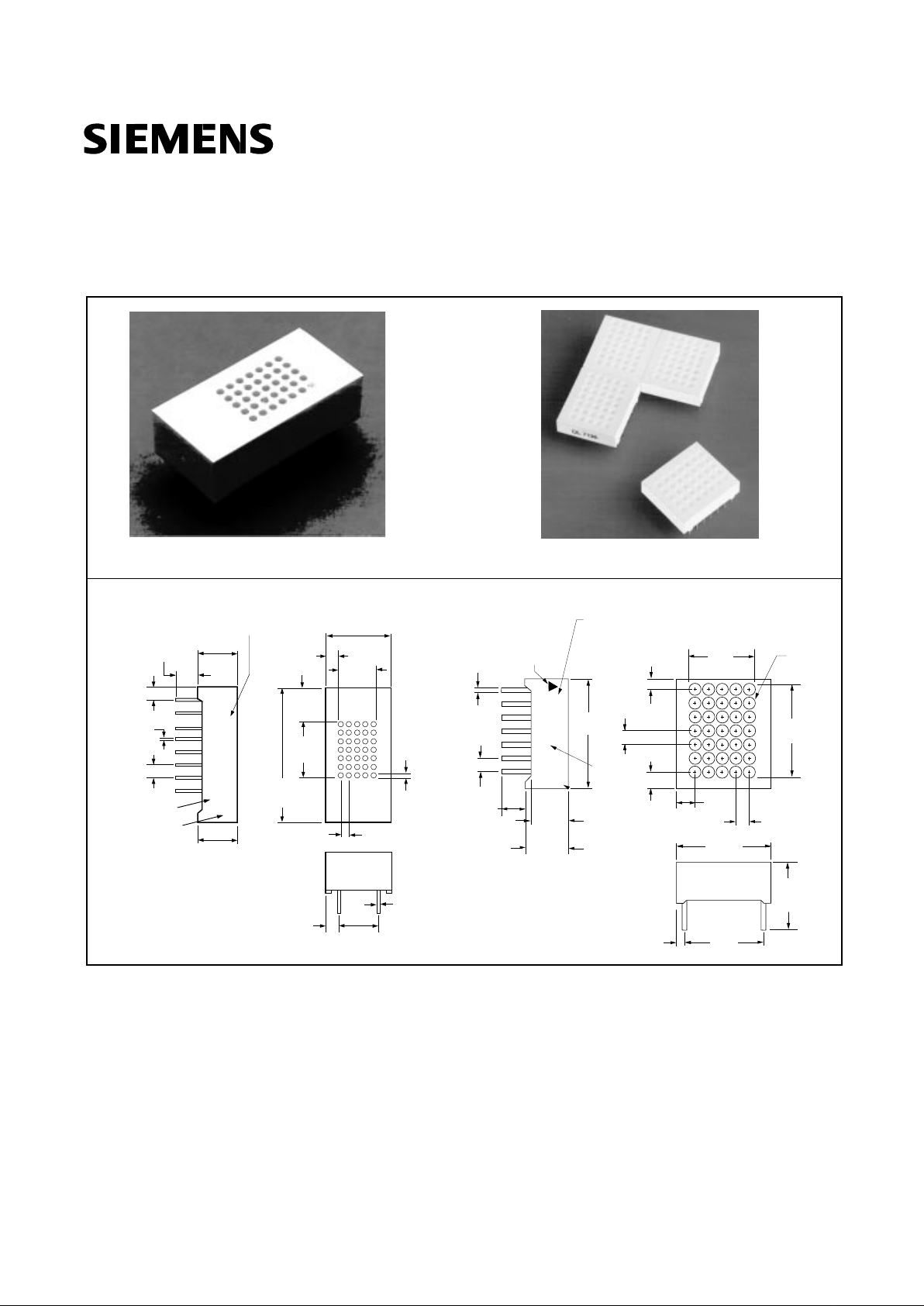
Package Dimensions in Inches (mm)
DLO4135/4137 DLO7135/7137
.043
(1.09)
.065 typ.
(.165)
.012
(.30)
.100
(2.54)
.300
(7.62)
.43
(10.92)
.235
(5.97)
.30
(7.62)
.100
(2.54)
.500 max.
(12.7)
DLO4135 Z
1.00 max.
(25.4)
DLO 4135
SIEMENS
▲
YYWW
Z
EIA date
code
Luminous
intensity code
Device marking
begins over pin 1
.14 min.
(3.56)
.310
(7.87)
.310
(7.87)
.
100 (2.54) typ.
0
.18 ± .02
(
4.57) (.51)
.100 (2.54)
SIEMENS YYWW
DLO7135
Z
Pin 1
indicator
Device marking
begins over
pin 1
.800
(20.32)
.125
(3.18)
1.00
(2.54)
typ.
.295
(7.49)
.018
(.45)
sq.
.325
(8.26)
EIA date
code
.080
(2.03)
diam. re
f.
.075
(1.91)
ref.
.150
(3.81)
.100
(2.54) typ.
.700
(17.78)
.50
(12.70)
ref.
.600
(15.24)
DLO7135 Z
Luminous
intensity
code
1.00
(2.54)
typ.
.050
(1.27)
.48
(12.19)
.68
(17.27)
.160
(4.06)
FEATURES
• 5x7 Dot Matrix Characters
DLO4135/DLG4137: .43" High
DLO7135/DLG7137: .68" High
• Wide Viewing Angle ± 75 °
• 96 Character ASCII Set
Upper Case and Lower Case Characters
• Fully Encapsulated, Rugged Solid Plastic Package
• Built-in Memory
• Built-in Character Generator
• Built-in Multiplex and LED Drive Circuitry
• Built-in Lamp Test
• Intensity Control (4 levels)
• Microprocessor Bus Compatible
• Intensity Coded for Display Uniformity
• Single 5-Volt Power Supply
• X/Y Stackable
• Available in High Efficiency Red and Green
Page 2
2–9
DLO4135/7135/DLG4137/7137
DESCRIPTION
The DLX413X/DLX713X are single digit 5x7 dot matrix
Intelligent Display devices. The DLX413X character is
0.43" high. The DLX713X character is 0.68" high. The builtin CMOS integrated circuit contains memory, ASCII character generator, LED multiplexing and drive circuitry;
thereby eliminating the need for additional circuitry. They
will display the 96 ASCII characters.
These devices are TTL and microprocessor compatible
and offer the possibility of cascading the displays, allowing
for multi-character messages. These displays were
designed for viewing distances of up to 20 feet(DLX413X)
or 30 feet (DLX713X). They require a single 5-volt power
supply and parallel ASCII input.
All products are 100% tested, then subjected to out-going
AQLs of .25% for brightness matching, visual alignment
and dimensions, .065% for electrical and functional.
Important:
Refer to Appnote 18, “Using and Handling
Intelligent Displays.” Since this is a CMOS device, normal
precautions should be taken to avoid static damage.
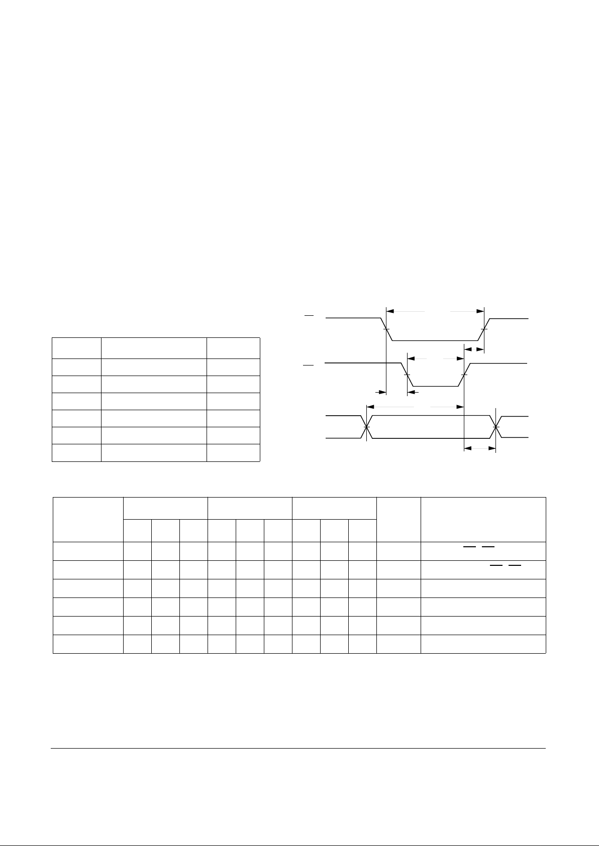
Timing Parameters at 25 ° C, V
CC
=5.0 V ± 0.5 V
Symbol Parameter Units (ns)
T
CES
Chip Enable Set-Up 10
T
DS
Data Set Up 100
T
W
Write Pulse 120
T
DH
Data Hold 20
T
CEH
Chip Enable Hold 20
T
ACC
Access Time 150
DC Characteristics
Notes
1. “Off Axis Viewing Angle” definition: The minimum angle in any direction from the normal to the display surface at which any part of any dot
in the display is not visible.
2. This display contains a CMOS integrated circuit. Normal CMOS handling precautions should be taken to a void damage due to high
static voltages or electric fields. See Appnote 18.
3. Unused inputs must be tied to an appropriate logic voltage level (either V + or GND).
4. V
CC
=5.0 VDC ± 10%.
5. Clean only in water, isopropyl alcohol, freon TF, TE (or equivalent).
Parameter
–40 ° C +25 ° C +85 ° C
Units Conditions
Min. Typ. Max. Min. Typ. Max. Min. Typ. Max.
I
CC
(20 dots on) 135 180 100 140 85 115 mA V
CC
=5 V,
BL0
=
BL1
=5 V
I
CC
Blank 2.0 5.5 1.5 4.0 0.8 3.5 mA V
CC
=WR=5.0 V,
BL0
=
BL1
=0 V
I
IL
(all inputs) 25 50 100
µ AV
IN
=0.8 V, V
CC
=5 V ± 0.5 V
V
IH
2.0 2.0 2.0 V V
CC
=5 V ± 0.5 V
V
IL
0.8 0.8 0.8 V V
CC
=5 V ± 0.5 V
V
CC
4.5 5.0 5.5 4.5 5.0 5.5 4.5 5.0 5.5 V
Maximum Ratings
V
CC
Range (max.) . . . . . . . . . . . . . . . . . . . . . .–0.5 to +7.0 Vdc
Voltage, Any Pin, Respect to GND. . . . . . –0.5 to V
CC
+0.5 Vdc
Operating Temperature . . . . . . . . . . . . . . . . . . –40 °
C to +85 ° C
Storage Temperature . . . . . . . . . . . . . . . . . . . –40 °
C to +100 ° C
Maximum Solder Temperature, .063"
below Seating Plane, t<5 sec. . . . . . . . . . . . . . . . . . . . 260 °
C
Relative Humidity at 85 °
C (non condensing). . . . . . . . . . . 85%
Optical Characteristics (Typical) at 25 ° C
Time Averaged Luminous Intensity/Dot at 5 V. . 1500 mcd typ.
Character Size
DLO4135/DLG4137 . . . . . . . . . . . . . . . . . . . . . . . . . . . . 0.43"
DLO7135/DLG7137 . . . . . . . . . . . . . . . . . . . . . . . . . . . . 0.68"
Viewing Angle (Note 1). . . . . . . . . . . . . . . . . . . . . . . . . . . . ±
75 °
Spectral Peak Wavelength
DLO4135/7135 (High Efficiency Red) . . . . . . . . .635 nm typ.
DLG4137/7137 (Green) . . . . . . . . . . . . . . . . . . . .565 nm typ.
Dot to Dot Intensity Ratio . . . . . . . . . . . . . . . . . . . . 1.8:1.0 max.
Timing Characteristics — Write Cycle Waveforms
T
ACC
T
CEH
T
W
T
CES
T
DH
T
DS
CE
WE
DATA
Page 3
2–10
DLO4135/7135/DLG4137/7137
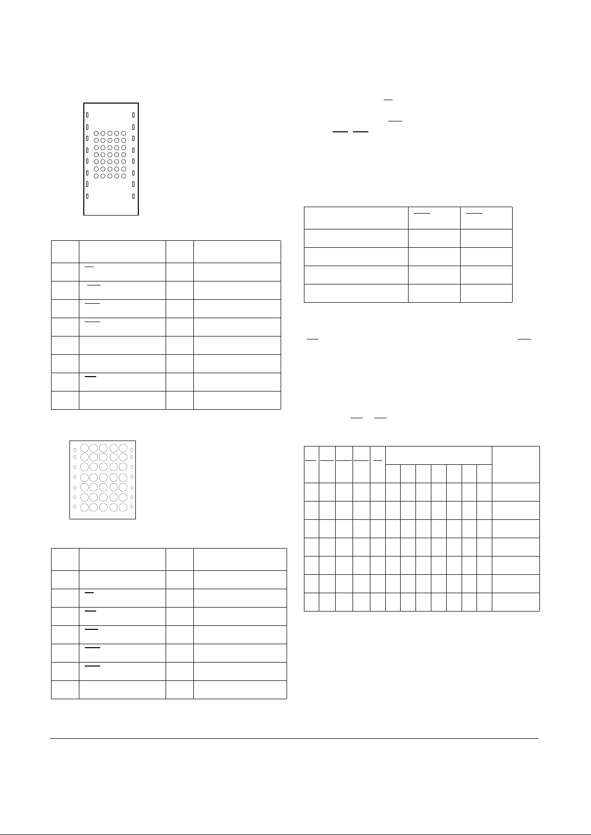
Top View — DLO4135/DLG4137
Pin Functions — DLO4135/DLG4137
Top View — DLO7135/DLG7137
Pin Functions — DLO7135/DLG7137
Pin Function Pin Function
1LT Lamp 9 D0 Data LSB
2 WR
Write 10 D1 Data
3 BL1
Brightness 11 D2 Data
4 BL0
Brightness 12 D3 Data
5 No Pin 13 D4 Data
6 No Pin 14 D5 Data
7CE
Chip Enable 15 D6 Data MSB
8 GND 16 +V
CC
Pin Function Pin Function
1V
CC
8 D0 Data Input LSB
2L
T Lamp Test 9 D1 Data
3CE
Chip Enable 10 D2 Data
4WR
Write 11 D3 Data
5 BL1
Brightness 12 D4 Data
6 BL0
Brightness 13 D5 Data
7 GND 14 D6 Data Input MSB
1
6
1
5
1
4
1
3
1
2
1
1
1
0
9
1
2
3
4
5
6
7
8
1
2
3
4
5
6
7
1
4
1
3
1
2
1
1
1
0
9
8
Lamp Test
When the lamp test (LT) is activated, all dots on the display
are illuminated at
1
⁄
7
brightness. The lamp test function is
independent of write (WR
) and the settings of the blanking
inputs (BL0
, BL1).
This convenient test gives a visual indication that all dots are
functioning properly . Lamp test also may be used as a cursor
function or pointer which does not destroy previously displayed characters.
Dimming and Blanking the Display
Loading Data
Loading data into the display is straightforward. Chip enable
(CE
) should be present and stable during a write pulse (WR).
Parallel data information should be stable for the minimum
time (T
W
) and held for TDH after write has gone high. No synchronization is necessary and each character will continue to
be displayed until it is replaced with another. Multiple displays may be stacked together with only an additional
decoder IC for chip enable decoding.
Note : Either BL0 or BL1 should be held high for display to light up.
Data Loading Example
X=don’t care, NC=no change
Brightness Level BL1
BL0
Blank 0 0
1
⁄
7
Brightness 0 1
1
⁄
2
Brightness 1 0
Full Brightness 1 1
CE WR BL0 BL1 LT
Data Input
D6 D5 D4 D3 D2 D1 D0
H X H X H X X X X X X X NC
X X L L H X X X X X X X Blank
X X X X L X X X X X X X Lamp Test
L L H H H H L L L L L H A
L L H H H H H H L L H L r
L L H H H L H H L L H H 3
L L H H H L H L H L H H +
Page 4
2–11
DLO4135/7135/DLG4137/7137
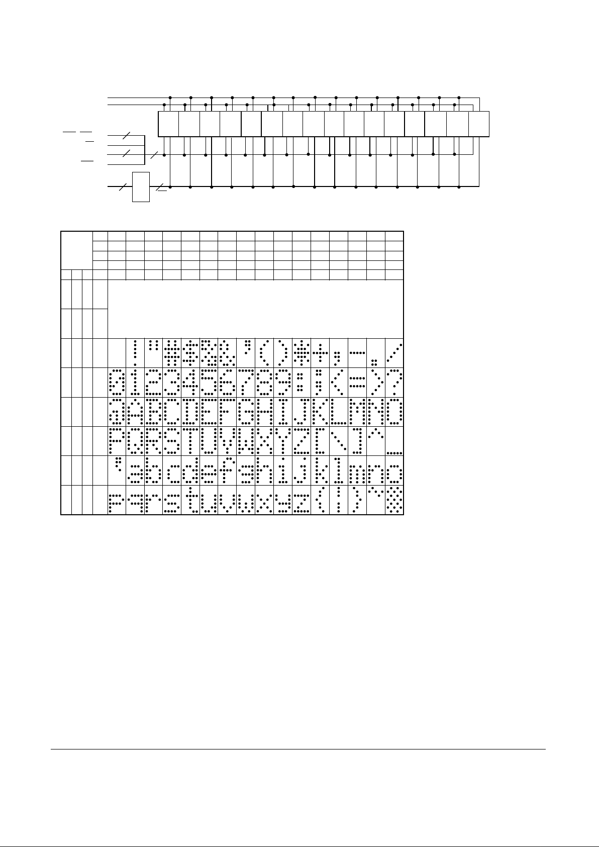
16 Digits Interconnection
Character Set
D15
+5
GND
BL0-BL1
LT
D0-D6
WR
A0-A3
2
7
4
11
16
CE
D0
ASCII
CODE
D0
D1
D2
D3
0
0
0
0
0
1
0
0
0
1
0
1
0
0
2
1
1
0
0
3
0
0
1
0
4
1
0
1
0
5
0
1
1
0
6
1
1
1
0
7
0
0
0
1
8
1
0
0
1
9
0
1
0
1
A
1
1
0
1
B
0
0
1
1
C
1
0
1
1
D
0
1
1
1
E
1
1
1
1
F
0
0
0
0
1
1
1
1
0
0
1
1
0
0
1
1
0
1
0
1
0
1
0
1
0
1
2
3
4
5
6
7
D6 D5 D4 HEX
Notes: 1. High = 1 level.
2. Low = 0 level.
3. Upon power up, the device will initialize in a random state.
THESE CODES DISPLAY BLANK
 Loading...