

Datasheet DK1a1b-L2-9V, DK1a1b-L2-5V, DK1a1b-L2-3V, DK1a1b-L2-24V, DK1a1b-L2-12V Datasheet (NAIS)
...Page 1
VDE
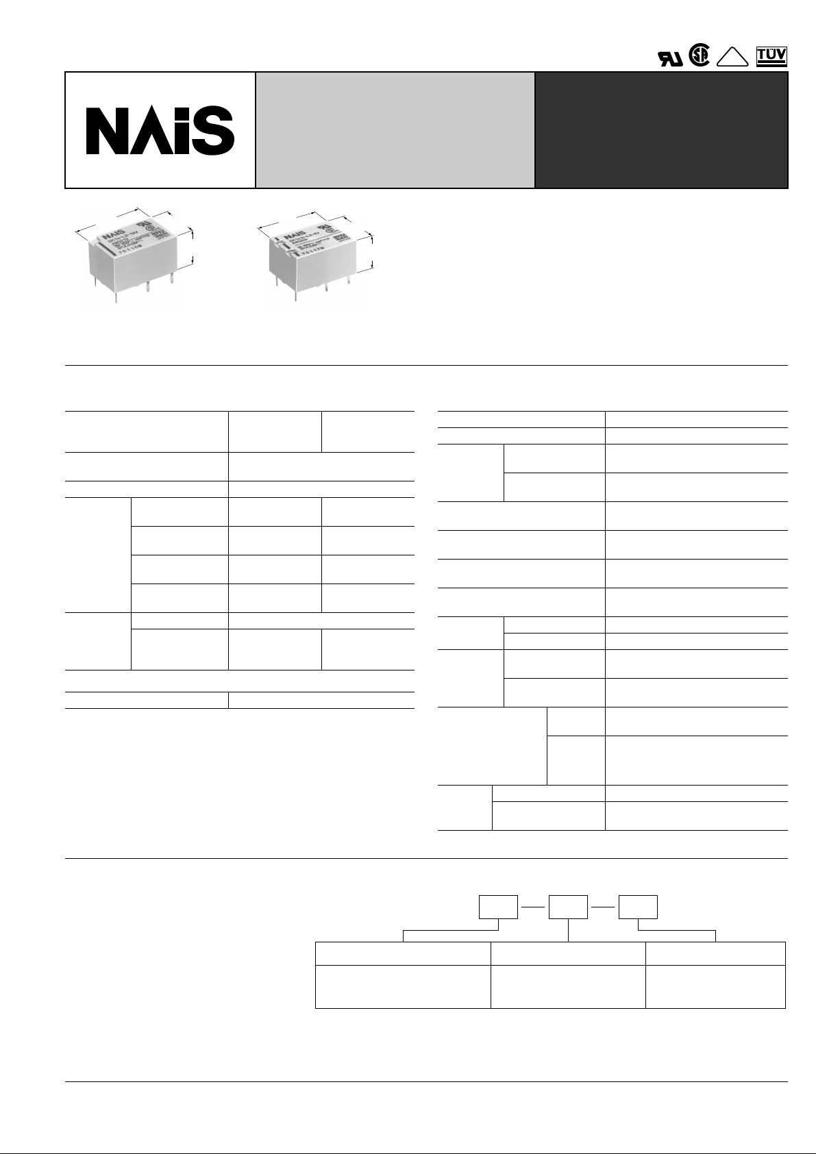
MINIATURE POWER RELAY
20
.787
12.5
.492
10
.394
20
.787
1a 1a1b
15
.591
10
.394
mm inch
SPECIFICATIONS
Contact
Arrangement 1 Form A
Initial contact resistance, max.
(By voltage drop 6 V DC 1A)
Contact material Gold flash over silver alloy
Rating
(resistive)
Expected
life (min.
operations)
Nominal
switching capacity
Max. switching
power
Max. switching
voltage
Max. switching
current
Mechanical 5 × 10
Electrical
(resistive)
10 A 250 V AC
10 A 30 V DC
300 W, 2,500 VA 240 W, 2,000 VA
250 V AC,
30 V DC
10 A 8 A
5
10
(10 A 250 V AC,
10 A 30 V DC)
Coil
Nominal operating power 200 mW
Remarks
* Specifications will vary with foreign standards certification ratings.
1
*
Measurement at same location as "Initial breakdown voltage" section
2
Detection current: 10 mA
*
3
*
Wave is standard shock voltage of ± 1.2 × 50 µ s according to JEC-212-1981
4
Excluding contact bounce time
*
5
*
Half-wave pulse of sine wave: 11ms; detection time: 10 µ s
6
Half-wave pulse of sine wave: 6ms
*
7
*
Detection time: 10 µ s
8
*
Refer to 5. Conditions for operation, transport and storage mentioned in
AMBIENT ENVIRONMENT (Page 61).
2 Form A,
1 Form A
1 Form B
30 m Ω
8 A 250 V AC
8 A 30 V DC
250 V AC,
30 V DC
7
10
(8 A 250 V AC,
8 A 30 V DC)
DK-RELAYS
FEATURES
• Large capacity in small size: 10 A 250 V AC (1a)
• High sensitivity: 200 mW nominal operating power
• High breakdown voltage 4,000 Vrms between contacts and
coil 1,000 Vrms between open contacts Meeting FCC P art 68
• Sealed construction
• Latching types available
Characteristics
Max. operating speed 20 cpm (at rated load)
Initial insulation resistance*
Initial
breakdown
voltage*
Surge voltage between coil and
contact*
Operate time*
Between open
contacts
Between contacts
2
and coil
3
4
1
(at nominal voltage)
Release time (without diode)*
(at nominal voltage)
Temperature rise
(at nominal voltage)
5
Shock
resistance
Vibration
resistance
Functional*
Destructive*
Functional*
Destructive
Conditions for operation, transport and
storange*
8
(Not freezing and
condensing at low
5
6
7
Ambient
temp.
Humidity 5 to 85% R.H.
temperature)
Unit
weight
1 Form A Approx. 5.6 g .20 oz
1 Form A 1 Form B,
2 Form A
Min. 1,000 m Ω (at 500 V DC)
1,000 Vrms
4,000 Vrms
Min. 10,000 V
Max. 10 ms (Approx. 5 ms)
4
Max. 8 ms (Approx. 3 ms)
Max. 40 ° C with nominal coil voltage
and at 10 A switching current
Min. 98 m/s
Min. 980 m/s
88.2 m/s
2
{10 G}
2
{100 G}
2
{9 G}, 10 to 55 Hz
at double amplitude of 1.5 mm
176.4 m/s
2
{18 G}, 10 to 55 Hz
at double amplitude of 3.0 mm
–40 ° C to +65 ° C
–40 ° F to +149 ° F
Approx. 6 g .21 oz
TYPICAL
APPLICATIONS
• Switching power supply
• Power switching for various
OA equipment
• Control or driving relays for industrial
machines (robotics, numerical control
machines, etc.)
• Output relays for programmable logic
controllers, temperature controllers,
timers and so on.
• Home appliances
ORDERING INFORMATION
Ex. DK
Contact arrangement
1a: 1 Form A
2a: 2 Form A
1a1b: 1 Form A 1 Form B
Note: Standard packing Carton: 50 pcs.; Case: 500 pcs.
UL/CSA, TÜV approved type is standard.
1a L2 12V
Operating function Coil voltage
Nil: Single side stable
L2: 2 coil latching
3, 5, 6, 9, 12, 24V
239
Page 2
Ω ( ±
Ω ( ±
DK
TYPES AND COIL DATA (at 20 ° C 68 ° F)
Single side stable
DK1a-3V 3 2.1 0.3 66.6 45 200 3.9
DK1a-5V 5 3.5 0.5 40 125 200 6.5
1 Form A
1 Form A
1 Form B
2 Form A
DK1a-6V 6 4.2 0.6 33.3 180 200 7.8
DK1a-9V 9 6.3 0.9 22.2 405 200 11.7
DK1a-12V 12 8.4 1.2 16.6 720 200 15.6
DK1a-24V 24 16.8 2.4 8.3 2,880 200 31.2
DK1a1b-3V 3 2.1 0.3 66.6 45 200 3.9
DK1a1b-5V 5 3.5 0.5 40 125 200 6.5
DK1a1b-6V 6 4.2 0.6 33.3 180 200 7.8
DK1a1b-9V 9 6.3 0.9 22.2 405 200 11.7
DK1a1b-12V 12 8.4 1.2 16.6 720 200 15.6
DK1a1b-24V 24 16.8 2.4 8.3 2,880 200 31.2
DK2a-3V 3 2.1 0.3 66.6 45 200 3.9
DK2a-5V 5 3.5 0.5 40 125 200 6.5
DK2a-6V 6 4.2 0.6 33.3 180 200 7.8
DK2a-9V 9 6.3 0.9 22.2 405 200 11.7
DK2a-12V 12 8.4 1.2 16.6 720 200 15.6
DK2a-24V 24 16.8 2.4 8.3 2,880 200 31.2
2 coil latching
DK1a-L2-3V 3 2.1 2.1 66.6 66.6 45 45 200 200 3.9
DK1a-L2-5V 5 3.5 3.5 40 40 125 125 200 200 6.5
1 Form A
1 Form A
1 Form B
2 Form A
DK1a-L2-6V 6 4.2 4.2 33.3 33.3 180 180 200 200 7.8
DK1a-L2-9V 9 6.3 6.3 22.2 22.2 405 405 200 200 11.7
DK1a-L2-12V 12 8.4 8.4 16.6 16.6 720 720 200 200 15.6
DK1a-L2-24V 24 16.8 16.8 8.3 8.3 2,880 2,880 200 200 31.2
DK1a1b-L2-3V 3 2.1 2.1 66.6 66.6 45 45 200 200 3.9
DK1a1b-L2-5V 5 3.5 3.5 40 40 125 125 200 200 6.5
DK1a1b-L2-6V 6 4.2 4.2 33.3 33.3 180 180 200 200 7.8
DK1a1b-L2-9V 9 6.3 6.3 22.2 22.2 405 405 200 200 11.7
DK1a1b-L2-12V 12 8.4 8.4 16.6 16.6 720 720 200 200 15.6
DK1a1b-L2-24V 24 16.8 16.8 8.3 8.3 2,880 2,880 200 200 31.2
DK2a-L2-3V 3 2.1 2.1 66.6 66.6 45 45 200 200 3.9
DK2a-L2-5V 5 3.5 3.5 40 40 125 125 200 200 6.5
DK2a-L2-6V 6 4.2 4.2 33.3 33.3 180 180 200 200 7.8
DK2a-L2-9V 9 6.3 6.3 22.2 22.2 405 405 200 200 11.7
DK2a-L2-12V 12 8.4 8.4 16.6 16.6 720 720 200 200 15.6
DK2a-L2-24V 24 16.8 16.8 8.3 8.3 2,880 2,880 200 200 31.2
Part No.
Part No.
Nominal
voltage,
V DC
Nominal
voltage,
V DC
Pick-up
voltage,
V DC (max.)
Set voltage,
V DC (max.)
V DC (min.)
Reset voltage,
V DC (max.)
Drop-out
voltage,
Nominal
operating
current,
mA ( ± 10%)
Nominal
operating
current,
mA ( ± 10%)
Set Reset Set Reset Set Reset
Coil
resistance,
10%)
Coil
resistance,
10%)
Nominal
operating
power,
mW
Nominal
operating
power,
mW
Maximum
allowable
voltage,
V DC (at 65 ° C
149°F)
Maximum
allowable
voltage,
V DC (at 65 ° C
149°F)
240
Page 3

80 90 10 110 120 130 140
0
1
2
3
4
5
6
7
8
9
Coil applied voltage,%V
Operate/release time, ms
Release time
(with diode)
Operate time
Release time
x
x
Max.
Min.
Max.
Max.
Min.
Min.
x
0
10
20
30
Operate/release time, ms
Distribution frequency
123456
Operate time
Release time
REFERENCE DATA
1. 1 Form A type
1. Maximum operating power 2. Life curve 3. Operate/Release time
100
1,000
Sample: DK1a-24V, 5 pcs.
DK
AC inductive load
10
1
Contact current, A
0.1
(cosϕ= 0.4)
DC inductive load
(L/R = 7 ms)
10 100 1,000
AC resistive load
DC resistive
load
Contact voltage, V
4. Coil temperature rise (at 30 ° C 68 ° F)
Sample: DK1a-12V, 5 pcs.
50
40
30
20
Coil temperature rise, °C
10
0
80 90 100 110 120 130
Coil applied voltage,%V
10 A
7 A
5 A
0 A
100
4
Life, ×10
10
250 V AC inductive load (cosϕ= 0.4)
30 V DC inductive load (L/R = 7 ms)
1
012345678910
250 V AC resistive load
30 V DC resistive load
Contact voltage, V
5. Ambient temperature characteristics
Sample: DK1a-24V, 6 pcs
Ambient temperature: -40 ° C to +80 ° C –40 ° F to
+176 ° F
130
Drop-out
voltage
120
110
Variation ratio, %
100
20
90
80
70
Pick-up
voltage
40 60 800–20–40
Ambient
temperature,°C
6. Operate/Release time (at 20 ° C 68 ° F)
Sample: DK1a-24V (50 pcs.)
7. Contact resistance (at 20 ° C 68 ° F)
Sample: DK1a-24V (50 pcs.)
26
24
22
20
18
16
14
12
Distribution frequency
10
8
6
4
2
0
1.5
2. 1 Form A 1 Form B type, 2 Form A type
1. Maximum operating power 2. Life curve 3. Operate/Release time (at 20 ° C 68 ° F)
AC inductive load
10
5
DC inductive load
Contact current, A
1
0.1
2.5
3.5
2.0
Contact resistance, mΩ
(cosϕ= 0.4)
(L/R = 7 ms)
10 100 1,000
4.5
3.0
4.0
5.0
AC resistive load
DC resistive
load
Contact voltage, V
Sample: DK1a1b-12V, 5 pcs.
1,000
100
4
250 V AC resistive load
Life, ×10
10
250 V AC inductive load (cosϕ= 0.4)
30 V DC inductive load (L/R = 7 ms)
1
012345678910
30 V DC resistive load
Contact current, A
9
8
7
6
5
Operate time
4
3
Operate/release time, ms
2
1
0
80 90 10 110 120 130 140
Release time
(with diode)
Release time
Coil applied voltage,%V
Max.
x
Min.
Max.
x
Min.
Max.
x
Min.
241
Page 4

DK
134
865
-
+
134
865
-
+
4. Coil temperature rise
Sample: DK1a1b-12V, 5 pcs.
Ambient temperature: 20 ° C 68 ° F
50
40
30
20
Coil temperature rise, °C
10
0
80 90 100 110 120 130
Coil applied voltage,%V
8 A
5 A
0 A
5. Ambient temperature characteristics
Pick-up
voltage
130
120
110
Variation ratio, %
100
40 60 800–20–40
Drop-out
voltage
Ambient
temperature,°C
20
90
80
70
DIMENSIONS
1. 1 Form A type
9.7
.382
0.3
.012
0.4
.016
9.7
.382
0.3
.012
0.4
.016
2.54
.100
2. 1 Form A 1 Form B type, 2 Form A type
.787
9.7
.382
0.3
.012
0.4
.016
10.16
.400
0.8
.031
Single side stable type
20
.787
0.8
.031
7.62
10.16
.300
.400
2 coil latching type
20
.787
0.8
0.4
.031
.016
7.62
7.62
.300
.300
General tolerance: ± 0.3 ± .012
Single side stable type
20
0.8
.031
1.11
7.62
.044
.300
3.5
.138
2.42
.095
0.8
.031
1.11
.044
0.8
.031
1.11
.044
3.5
.138
3.5
.138
1.2
.047
1.2
.047
15
.591
10.16
.400
PC board pattern (Copper-side view)
12.5
.492
10.16
.400
12.5
.492
10.16
.400
2.54
.100
10.16
0.4
.016
0.4
.016
.400
10.16
.400
2.54
.100
The above shows 2 coil latching type.
No.5 terminal is eliminated on single side
7.62
.300
7.62
.300
stable type.
Tolerance: ± 0.1 ± .004
PC board pattern (Copper-side view)
7.62
.300
.043 dia.
0.4
.016
10.16
.400
10.16
.400
7.62
.300
7.62
.300
1.1 dia.
(Deenergized condition)
Schematic
1.1 dia.
.043 dia.
(Bottom view)
Single side stable
(Deenergized condition)
134
-
+
6
1.1 dia.
.043 dia.
2 coil latching
(Reset condition)
134
-
++
65
Since this is a polarized relay ,
the connection to the coil
should be done according to
the above schematic.
Schematic (Bottom view)
<1 Form A 1 Form B type>
Single side stable
mm inch
2 coil latching
(Reset condition)
134
-
+7+
865
242
2 coil latching type
.012
0.3
9.7
.382
0.4
.016
2.54
.100
0.6
.024
7.62
.300
20
.787
0.8
.031
7.62
.300
0.8
.031
1.11
.044
3.5
.138
2.42
.095
15
.591
10.16
.400
Note:
Relay out-line and PC board pattern are common for both
1 Form A 1 Form B type and 2 Form A type.
General tolerance: ± 0.3 ± .012
0.4
.016
2.54
.100
10.16
.400
7.62
.300
Tolerance: ± 0.1 ± .004
7.62
.300
1.1 dia.
.043 dia.
Single side stable
(Deenergized condition)
Since this is a polarized relay, the connection
to the coil should be done according to the
above schematic.
2 coil latching
(Reset condition)
134
-
+7+
865
<2 Form A>
Page 5

DK relay socket TYPES AND RELAY COMPATIBILITY
Socket 1 Form A 1 Form A 1 Form B, 2 Form A
Relay
1 Form A
1 Form A 1 Form B
2 Form A
Single side
stable type
Single side stable type DK1a-PS DK1a-PSL2 — —
2 coil latching type — DK1a-PSL2 — —
Single side stable type — — DK2a-PS DK2a-PSL2
2 coil latching type — — — DK2a-PSL2
2 coil
latching type
Single side
stable type
SPECIFICATIONS
Breakdown voltage*
Insulation resistance Min. 1,000 mΩ (at 500 V DC)
Heat resistance 150°C (for 1 hour)
Max. continuous current 10 A (DK1a-PS, DK1a-PSL2), 8 A (DK2a-PS, DK2a-PSL2)
Remarks
*1Detection current: 10 mA
1
4,000 Vrms (Except the portion between coil terminals)
DIMENSIONS
1 Form A type
1 Form A 1 Form B type, 2 Form A type
PC board pattern (Copper-side view)
1 Form A
DK
2 coil
latching type
mm inch
15±0.6
.591±.024
13.7±0.6
.539±.024
0.3±0.1
.012±.004
2.54±0.1
.100±.004
23±0.6
.906±.024
7.62±0.3
.300±.012
0.8
.031
7.62±0.3
.300±.012
17±0.6
.669±.024
6±0.3
.236±.012
3.4±0.3
.134±.012
0.25
.010
10.16±0.3
.400±.012
15±0.6
.591±.024
17±0.6
.669±.024
6±0.3
.236±.012
3.4±0.3
.134±.012
FIXING AND REMOVAL METHOD
1. Match the direction of relay
and socket.
2. Both ends of the rela y are to
be secured firmly so that the
socket hooks on the top surface of the relay.
23±0.6
.906±.024
13.7±0.6
.539±.024
0.3±0.1
7.62±0.3
.300±.012
10.16±0.3
.400±.012
.012±.004
General tolerance: ±0.3 ±.012
3. Remo ve the relay , applying
force in the direction shown
below.
10.16±0.3
.400±.012
12
65
2.54
.100
43
1.2 dia.
.047 dia.
2.54
.100
1 Form A 1 Form B
1.2 dia.
12
87
The above shows 2 coil latching type. No.2 and 5
terminal are eliminated on single side stable type.
43
.047 dia.
65
2.54
.100
2.54
.100
Tolerance: ±0.1 ±.004
4. In case there is not enough
space to grasp relay with fingers, use screwdrivers in the
way shown below.
GOOD NO GOOD
NOTES
1. Phase synchronization of AC-load
switching
In case of switching the contact synchronized with phase of load voltage, the lif e of
contact might be shorter or contact failure
might be caused. Please confirm this
matter in the actual system in this case. If
necessary, the phase control would be
recommended.
Vin
Load
voltage
Vin
Ry
Load
Load
voltage
2. Soldering should be done under the f ollowing conditions:
250°C 482°F within 10s
300°C 572°F within 5s
350°C 662°F within 3s
For Cautions for Use, see Relay Technical Information (Page 48 to 76).
9/1/2000 All Rights Reserved, © Copyright Matsushita Electric Works, Ltd.
Go To Online Catalog
243
 Loading...