

Datasheet DG405AZ, DG405AK, DG403DY, DG403DK, DG403DJ Datasheet (Maxim Integrated Producs)
...Page 1
_______________General Description
Maxim's redesigned DG401/DG403/DG405 analog
switches now feature guaranteed low on-resistance
matching between switches (2Ω max) and guaranteed
on-resistance flatness over the signal range (3Ω max).
These low on-resistance switches (20Ω typ) conduct
equally well in either direction and are guaranteed to
have low charge injection (15pC max). The new design
offers lower off leakage current over temperature (less
than 5nA at +85°C).
The DG401/DG403/DG405 are dual, high-speed
switches. The single-pole/single-throw DG401 and
double-pole/single-throw DG405 are normally open
dual switches. The dual, single-pole/double-throw
DG403 has two normally open and two normally closed
switches. Switching times are 150ns max for tONand
100ns max for t
OFF
, with a maximum power consumption of 35µW. These devices operate from a single
+10V to +30V supply, or bipolar supplies of ±4.5V to
±20V. Maxim's improved DG401/DG403/DG405 are
fabricated with a 44V silicon-gate process.
________________________Applications
Sample-and-Hold Circuits Test Equipment
Guidance and Control Systems Heads-Up Displays
Communications Systems PBX, PABX
Battery-Operated Systems Audio Signal Routing
Military Radios
______________________New Features
♦
Plug-In Upgrade for Industry-Standard
DG401/DG403/DG405
♦ Improved r
DS(ON)
Match Between Channels (2Ω max)
♦ Guaranteed r
FLAT(ON)
Over Signal Range (3Ω max)
♦ Improved Charge Injection (15pC max)
♦ Improved Off Leakage Current Over Temperature
(<5nA at +85°C)
__________________Existing Features
♦
Low r
DS(ON)
(30Ω max)
♦ Single-Supply Operation +10V to +30V
Bipolar-Supply Operation ±4.5V to ±20V
♦ Low Power Consumption (35µW max)
♦ Rail-to-Rail Signal Handling Capability
♦ TTL/CMOS-Logic Compatible
______________Ordering Information
Ordering Information continued on last page.
*Contact factory for dice specifications.
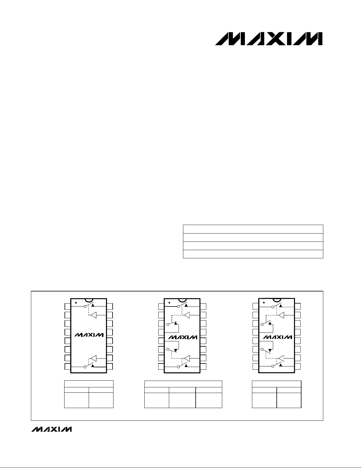
DG401/DG403/DG405
Improved, Dual, High-Speed Analog Switches
________________________________________________________________ Maxim Integrated Products 1
16
15
14
13
12
11
10
9
1
2
3
4
5
6
7
8
S1
IN1
VGND
N.C.
N.C.
N.C.
D1
TOP VIEW
DG401
V
L
V+
IN2
S2
D2
N.C.
N.C.
N.C.
16
15
14
13
12
11
10
9
1
2
3
4
5
6
7
8
S1
IN1
VGND
S3
D3
N.C.
D1
DG403
V
L
V+
IN2
S2
D2
N.C.
D4
S4
DIP/SO
DIP/SO
16
15
14
13
12
11
10
9
1
2
3
4
5
6
7
8
S1
IN1
VGND
S3
D3
N.C.
D1
DG405
V
L
V+
IN2
S2
D2
N.C.
D4
S4
DIP/SO
DG401
LOGIC SWITCH
0
1
OFF
ON
DG403
LOGIC SWITCHES 1, 2
0
1
OFF
ON
DG405
LOGIC SWITCH
0
1
OFF
ON
SWITCHES 3, 4
ON
OFF
SWITCHES SHOWN FOR LOGIC "0" INPUT N.C. = NOT INTERNALLY CONNECTED
LCC packages on last page.
_____________________Pin Configurations/Functional Diagrams/Truth Tables
19-4727; Rev 2; 6/99
PART TEMP. RANGE PIN PACKAGE
DG401CJ
0°C to +70°C 16 Plastic DIP
DG401CY 0°C to +70°C 16 Narrow SO
DG401C/D 0°C to +70°C Dice*
For free samples & the latest literature: http://www.maxim-ic.com, or phone 1-800-998-8800.
For small orders, phone 1-800-835-8769.
Page 2
TA= T
MIN
to T
MAX
V+ = 16.5V, V- = -16.5V,
VD= 15.5V,
V
S
= ±15.5V,
V+ = 16.5V, V- = -16.5V,
V
D
= ±15.5V,
V
S
= 15.5V
Improved, Dual, High-Speed Analog Switches
2 _______________________________________________________________________________________
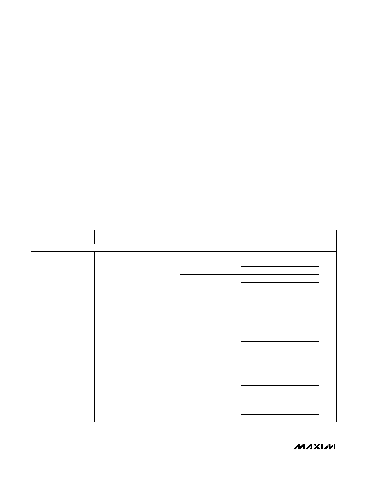
ABSOLUTE MAXIMUM RATINGS
ELECTRICAL CHARACTERISTICS
(V+ = 15V, V- = -15V, VL= +5V, GND = 0V, V
INH
= +2.4V, V
INL
= +0.8V, TA= T
MIN
to T
MAX
, unless otherwise noted.)
DG401/DG403/DG405
Note 1: Signals on S, D or IN exceeding V+ or V- are clamped by internal diodes. Limit forward current to maximum
current rating.
Stresses beyond those listed under “Absolute Maximum Ratings” may cause permanent damage to the device. These are stress ratings only, and functional
operation of the device at these or any other conditions beyond those indicated in the operational sections of the specifications is not implied. Exposure to
absolute maximum rating conditions for extended periods may affect device reliability.
Voltage Referenced to V-
V+.......................................................................................44V
GND ...................................................................................25V
V
L
.................................................(GND - 0.3V) to (V+ + 0.3V)
Digital Inputs, V
S
, VD(Note 1).......(V- - 2V) to (V+ + 2V) or 20mA
(whichever occurs first)
Continuous Current (any terminal)......................................30mA
Continuous Current, S or D.................................................20mA
Peak Current, S or D
(pulsed at 1ms, 10% duty cycle max) ..........................100mA
Continuous Power Dissipation (T
A
= +70°C)
16-Pin Plastic DIP(derate 10.53mW/°C above +70°C)...842mW
16-Pin Narrow SO (derate 8.70mW/°C above +70°C)...696mW
16-Pin CERDIP (derate 10.00mW/°C above 70°C).......800mW
20-Pin LCC (derate 9.09mW/°C above +70°C) ............727mW
Operating Temperature Ranges
DG40_C_ .............................................................0°C to +70°C
DG40_D_ ..........................................................-40°C to +85°C
DG40_A_ ........................................................-55°C to +125°C
Storage Temperature Range.............................-65°C to +150°C
Lead Temperature (soldering, 10sec).............................+300°C
PARAMETER
SYMBOL CONDITIONS
TEMP.
RANGE
MIN TYP MAX
(Note 2)
UNITS
Analog Signal Range V
ANALOG
(Note 3) -15 +15 V
C,D 20 45
A 20 30
C,D 55
Drain-Source
On-Resistance
r
DS(ON)
V+ = 13.5V, V- = -13.5V,
IS= -10mA,
V
D
= ±10V,
V
INH
= 2.4V,
V
INL
= 0.8V
A 45
Ω
0.5 2
Drain-Source
On-Resistance Match
Between Channels (Note 4)
∆r
DS(ON)
V+ = 15V, V- = -15V,
IS= -10mA,
V
D
= ±10V
C, D, A Ω
On-Resistance Flatness
(Note 4)
r
FLAT(ON)
V+ = 15V, V- = -15V,
I
S
= -10mA,
V
D
= ±5V, 0V
C, D, A
3
Ω
C, D -0.50 -0.01 0.50
A -0.25 -0.01 0.25
C, D -5 5
Source-Off
Leakage Current
(Note 7)
I
S(OFF)
A -10 10
nA
C, D -0.50 -0.01 0.50
A -0.25 -0.01 0.25
C, D -5 5
Drain-Off
Leakage Current
(Note 7)
I
D(OFF)
A -10 10
nA
C, D -1.0 -0.04 1.0
A -0.4 -0.04 0.4
C, D -10 10
Drain-On
Leakage Current
(Note 7)
I
D(ON)
or
I
S(ON)
V+ = 16.5V, V- = -16.5V,
V
D
= ±15.5V,
VS= ±15.5V
A -20 20
nA
TA= +25°C
TA= T
MIN
to T
MAX
TA= +25°C
TA= +25°C
TA= +25°C
TA= T
MIN
to T
MAX
TA= +25°C
TA= T
MIN
to T
MAX
TA= +25°C
TA= T
MIN
to T
MAX
TA= T
MIN
to T
MAX
3
6
±
SWITCH
±
Page 3

DG401/DG403/DG405
Improved, Dual, High-Speed Analog Switches
_______________________________________________________________________________________ 3
ELECTRICAL CHARACTERISTICS (continued)
(V+ = 15V, V- = -15V, VL= +5V, GND = 0V, V
INH
= +2.4V, V
INL
= +0.8V, TA= T
MIN
to T
MAX
, unless otherwise noted.)
Note 2: This data sheet uses the algebraic convention, where the most negative value is a minimum and the most positive value is a
maximum.
Note 3: Guaranteed by design.
Note 4:
∆rON= ∆rON(max) - ∆rON(min). On-resistance match between channels and flatness are guaranteed only with specified
voltages. Flatness is defined as the difference between the maximum and minimum value of on-resistance as measured at the
extremes of the specified analog signal range.
Note 5: Off isolation = 20log (V
S/VD
), VD= output, VS= input to off switch.
Note 6: Between any two switches.
Note 7: Leakage parameters I
S(OFF)
, I
D(OFF)
, and I
D(ON)
are 100% tested at the maximum rated hot temperature and guaranteed by
correlation at +25°C.
PARAMETER
SYMBOL CONDITIONS
MIN TYP MAX
(Note 2)
UNITS
Input Current with Input Voltage High I
INH
VIN= 2.4V, all others = 0.8V -1.0 0.005 1.0 µA
Input Current with Input Voltage Low I
INL
VIN= 0.8V, all others = 2.4V -1.0 0.005 1.0 µA
Power-Supply Range ±4.5 ±20 V
Positive Supply Current I+
All channels on or off,
V+ = 16.5V, V- = -16.5V,
V
IN
= 0V or 5V
TA= +25°C -1.0 0.01 1.0
µA
Negative Supply Current I-
All channels on or off,
V+ = 16.5V, V- = -16.5V,
VIN= 0V or 5V
TA= +25°C -1.0 0.01 1.0
µA
Logic Supply Current I
L
All channels on or off,
V+ = 16.5V, V- = -16.5V,
V
IN
= 0V or 5V
TA= +25°C -1.0 0.01 1.0
µA
Ground Current I
GND
All channels on or off,
V+ = 16.5V, V- = -16.5V,
V
IN
= 0V or 5V
TA= +25°C -1.0 0.01 1.0
µA
Turn-On Time t
ON
Figure 2 TA= +25°C 100 150 ns
Turn-Off Time t
OFF
Figure 2 TA= +25°C 60 100 ns
Break-Before-Make Delay (Note 3) t
D
DG403 only,
Figure 3
TA= +25°C 10 20 ns
Charge Injection (Note 3) Q
CL= 1.0nF, V
GEN
= 0V,
R
GEN
= 0Ω, Figure 4
TA= +25°C 10 15 pC
Off Isolation (Note 5) OIRR
RL= 100Ω, CL= 5pF,
f = 1MHz, Figure 5
TA= +25°C 72 dB
Crosstalk (Note 6)
RL= 50Ω, CL= 5pF,
f = 1MHz, Figure 6
TA= +25°C
90 dB
Source-Off Capacitance C
S(OFF)
f = 1MHz, Figure 7 TA= +25°C 12 pF
Drain-Off Capacitance C
D(OFF)
f = 1MHz, Figure 7 TA= +25°C 12 pF
Channel-On Capacitance
C
D(ON)
or C
S(ON)
f = 1MHz, Figure 8 TA= +25°C 39 pF
TA= T
MIN
to T
MAX
TA= T
MIN
to T
MAX
TA= T
MIN
to T
MAX
TA= T
MIN
to T
MAX
-5.0 5.0
-5.0 5.0
-5.0 5.0
-5.0 5.0
INPUT
SUPPLY
DYNAMIC
Page 4

DG401/DG403/DG405
Improved, Dual, High-Speed Analog Switches
4 _______________________________________________________________________________________
__________________________________________Typical Operating Characteristics
(TA = +25°C, unless otherwise noted.)
50
55
20
-20
ON-RESISTANCE vs. VD
(DUAL SUPPLIES)
25
45
MAX401-1
VD (V)
r
DS
(ON)
(Ω)
10
35
30
-10 0 20
40
15
10
5
A: V+ = 5V, V- = -5V
B: V+ = 10V, V- = -10V
C: V+ = 15V, V- = -15V
D: V+ = 20V, V- = -20V
A
B
C
D
35
5
-20
ON-RESISTANCE vs. VD AND
TEMPERATURE (DUAL SUPPLIES)
10
30
MAX401-2
VD (V)
r
DS
(ON)
(Ω)
20
20
15
-10 10
25
0
V+ = 15V, V- = -15V
TA = +125°C
TA = +85°C
TA = +25°C
TA = -55°C
140
20
0
ON-RESISTANCE vs. V
D
(SINGLE SUPPLY)
40
120
MAX401-3
VD (V)
r
DS
(ON)
(Ω)
20
80
60
515
100
10
V+ = 5V
V- = 0V
V+ = 10V
V+ = 15V
V+ = 20V
70
10
0
ON-RESISTANCE vs. VD AND
TEMPERATURE (SINGLE SUPPLY)
20
60
MAX401-4
VD (V)
r
DS
(ON)
(Ω)
20
40
30
515
50
10
V+ = 12V, V- = 0V
TA = +125°C
TA = +85°C
TA = +25°C
60
-60
-20 20
CHARGE INJECTION vs.
ANALOG VOLTAGE
-40
40
MAX401-7
VD (V)
Q (pC)
10
0
-20
-10 0
20
V+ = 15V, V- = -15V
100
0.0001
-55 125
SUPPLY CURRENT vs.
TEMPERATURE
0.001
10
MAX401-8
TEMPERATURE (°C)
I+, I-, I
L
(µA)
0.1
0.01
25
1
I+ at V+ = 16.5V
I- at V- = -16.5V
IL at VL = 5V
100
0.0001
-55 125
OFF LEAKAGE CURRENTS vs.
TEMPERATURE
0.001
10
MAX401-5
TEMPERATURE (°C)
OFF LEAKAGE (nA)
0.1
0.01
25
1
V+ = 16.5V
V- = -16.5V
VD = ±15V
V
S
= ±15V
100
0.0001
-55 125
ON LEAKAGE CURRENTS vs.
TEMPERATURE
0.001
10
MAX401-6
TEMPERATURE (°C)
ON LEAKAGE (nA)
0.1
0.01
25
1
V+ = 16.5V
V- = -16.5V
V
D
= ±15V
V
S
= ±15V
Page 5

DG401/DG403/DG405
Improved, Dual, High-Speed Analog Switches
_______________________________________________________________________________________ 5
__________Applications Information
_____________________Pin Description
Figure 1. Overvoltage Protection Using External Blocking Diodes
Operation with Supply Voltages
Other than ±15V
The DG401/DG403/DG405 switches operate with
±4.5V to ±20V bipolar supplies or with a +10V to +30V
single supply. In either case, analog signals ranging
from V+ to V- can be switched. The Typical Operating
Characteristics graphs illustrate typical analog-signal
and supply-voltage on-resistance variations. The usual
on-resistance temperature coefficient is 0.5%/°C (typ).
Logic Inputs
These devices operate with a single positive supply or
with bipolar supplies. They maintain TTL compatibility
with supplies anywhere in the ±4.5V to ±20V range as
long as VL= +5V. If VLis connected to V+ or another
supply at voltages other than +5V, the devices will
operate at CMOS-logic-level inputs.
Overvoltage Protection
Proper power-supply sequencing is recommended for
all CMOS devices. Do not exceed the absolute
maximum ratings because stresses beyond the listed
ratings may cause permanent damage to the devices.
Always sequence V+ on first, followed by V
L
, V-, and
logic inputs. If power-supply sequencing is not
possible, add two small, external signal diodes in
series with supply pins for overvoltage protection
(Figure 1). Adding diodes reduces the analog-signal
range to 1V below V+ and 1V below V-, without affecting low switch resistance and low leakage
characteristics. Device operation is unchanged, and
the difference between V+ and V- should not exceed
+44V.
DG401
DIP/SO LCC
NAME FUNCTION
1, 8 2, 10 D1, D2 Drain (Analog Signal)
2-7
1, 3-9,
11, 16
N.C. Not internally connected
9, 16 12, 20 S2, S1 Source (Analog Signal)
10, 15 13, 19 IN2, IN1 Digital Logic Inputs
11 14 V+
Positive Supply-Voltage
Input—connected to
substrate
12 15 V
L
Logic Supply-Voltage Input
13 17 GND Ground
14 18 V-
Negative Supply-Voltage
Input
DG403
DIP/SO LCC
NAME FUNCTION
1, 8, 3, 6 2, 10, 4, 8 D1-D4 Drain (Analog Signal)
2, 7
1, 3, 6, 9,
11, 16
N.C. Not internally connected
11 14 V+
Positive Supply-Voltage
Input—connected to
substrate
12 15 V
L
Logic Supply-Voltage Input
13 17 GND Ground
14 18 V-
Negative Supply-Voltage
Input
DG405
DIP/SO LCC
NAME FUNCTION
1, 8, 3, 6 2, 10, 4, 8 D1-D4 Drain (Analog Signal)
2, 7
1, 3, 6, 9,
11, 16
N.C. Not internally connected
11 14 V+
Positive Supply-Voltage
Input—connected to
substrate
12 15 V
L
Logic Supply-Voltage Input
13 17 GND Ground
14 18 V- Negative Supply Voltage
16, 9, 4, 5
20, 12,
5, 7,
S1-S4 Source (Analog Signal)
10, 15 13, 19 IN2, IN1 Digital Logic Inputs
16, 9, 4, 5
20, 12,
5, 7,
S1-S4 Source (Analog Signal)
10, 15 13, 19 IN2, IN1 Digital Logic Inputs
V+
S
V
g
D
V-
Page 6

DG401/DG403/DG405
Improved, Dual, High-Speed Analog Switches
6 _______________________________________________________________________________________
______________________________________________Timing Diagrams/Test Circuits
50%
t
OFF
tr < 20ns
tf < 20ns
V
OUT
V
OUT
t
ON
0.9 x V
OUT
0.9 x V
OUT
+3V
0V
0V
LOGIC
INPUT
SWITCH
OUTPUT
LOGIC INPUT WAVEFORM IS INVERTED FOR
SWITCHES THAT HAVE THE OPPOSITE LOGIC
SENSE CONTROL.
+5V +15V
V
OUT
RL = 1000Ω
CL = 35pF
-15V
REPEAT TEST FOR IN2 AND S2
0V
GND
LOGIC
INPUT
V
D
= +10V (for tON)
V
D
= -10V (for t
OFF
)
FOR LOAD CONDITIONS, SEE Electrical Characteristics.
CL INCLUDES FIXTURE AND STRAY CAPACITANCE.
V
OUT
= V
D
R
L
RL + r
DS(ON)
V+V
L
V-
D
IN
S
( )
DG401
DG403
DG405
Figure 2. Switching Time
Figure 4. Charge Injection
Figure 3. Break-Before-Make Interval
LOGIC
INPUT
SWITCH
OUTPUT 1
SWITCH
OUTPUT 2
+3V
+5V
V
50%
0V
V
OUT1
0.9 x V
OUT
0V
V
OUT2
0V
t
D
0.9 x V
OUT
t
D
+10V
+10V
LOGIC
INPUT
CL INCLUDES FIXTURE AND STRAY CAPACITANCE.
L
D
D
IN
GND
0V
+15V
V-
-15V
V+
S
S
V
OUT2
R
L1
R
L2
C
L2
RL = 1000Ω
CL = 35pF
DG401
DG403
DG405
V
OUT1
C
L1
+5V +15V
∆V
OUT
V
OUT
IN
ON OFF ON
Q = (∆V
OUT
) (CL)
R
GEN
V
GEN
V
L
SD
GND
0V -15V
V+
V-
C
L
10nF
DG401
DG403
DG405
V
OUT
Page 7

DG401/DG403/DG405
Improved, Dual, High-Speed Analog Switches
_______________________________________________________________________________________ 7
_________________________________Timing Diagrams/Test Circuits (continued)
IN
0V or 2.4V
SIGNAL
GENERATOR
+15V +5V
C
C
V+
V
L
ANALYZER
CH A
CH B
S
R
L
100Ω
GND
D
C
-15V
C = 5pF
FREQUENCY
TESTED
1MHz
SIGNAL
GENERATOR
AUTOMATIC
SYNTHESIZER
ANALYZER
TRACKING
SPECTRUM
ANALYZER
OFF ISOLATION = 20log
V
S
V
D
V-
DG401
DG403
DG405
Figure 5. Off Isolation
Figure 6. Crosstalk
IN2
0V or 2.4V
SIGNAL
GENERATOR
+15V +5V
C
C
V
L
ANALYZER
CH A
CH B
R
L
100Ω
GND
C
V-
-15V
C = 5pF
FREQUENCY
TESTED
1MHz
SIGNAL
GENERATOR
AUTOMATIC
SYNTHESIZER
ANALYZER
TRACKING
SPECTRUM
ANALYZER
0V or 2.4V
IN1
50Ω
V+
D
D
S
S
DG401
DG403
DG405
Figure 7. Channel-Off Capacitance
V-
CAPACITANCE
METER
GND
C
-15V
IN
0V or 2.4V
C
C
+15V +5V
V+
V
L
S
D
DG401
DG403
DG405
Figure 8. Channel-On Capacitance
DG401
DG403
DG405
CAPACITANCE
METER
C
+15V +5V
V+
D
S
GND
V
V-
-15V
L
IN
C
0V or 2.4V
C
Page 8

___________________Chip Topography
D1 S1
D2
S2
IN1
VGND
V
L
V+
IN2
0.102”
(2.59mm)
D3
(DG403/DG405)
S3
(DG403/DG405)
S4
(DG403/DG405)
D4
(DG403/DG405)
0.070”
(1.78mm)
DG401/DG403/DG405
Improved, Dual, High-Speed Analog Switches
_Ordering Information (continued)
____Pin Configurations (continued)
* Contact factory for dice specifications.
**Contact factory for availability and processing to MIL-STD-883B.
DG401
LCC
DG403
14
15
16
17
18
5
6
7
8
3
2
1
20
19
9
101112
13
S3
D3 4
N.C.
S4
D4
VGND
N.C.
V
L
V+
N.C.
D1
N.C.S1IN1
N.C.
D2
N.C.
S2
IN2
14
15
16
17
184
5
6
7
8
3
2
1
20
19
9
101112
13
N.C.
N.C.
N.C.
N.C.
N.C.
VGND
N.C.
V
L
V+
N.C.
D1
N.C.
S1
IN1
N.C.
D2
N.C.
S2
IN2
TOP VIEW
DG405
14
15
16
17
184
5
6
7
8
3
2
1
20
19
9
101112
13
D3
S3
N.C.
S4
D4
VGND
N.C.
V
L
V+
N.C.
D1
N.C.S1IN1
N.C.
D2
N.C.
S2
IN2
20 LCC**-55°C to +125°CDG401AZ
16 CERDIP**-55°C to +125°CDG401AK
16 CERDIP-40°C to +85°CDG401DK
16 Narrow SO-40°C to +85°CDG401DY
16 Plastic DIP-40°C to +85°CDG401DJ
20 LCC**-55°C to +125°CDG405AZ
16 CERDIP**-55°C to +125°CDG405AK
16 CERDIP-40°C to +85°CDG405DK
16 Plastic DIP-40°C to +85°CDG405DJ
16 Narrow SO-40°C to +85°CDG405DY
Dice*0°C to +70°CDG405C/D
16 Narrow SO0°C to +70°CDG405CY
16 Plastic DIP0°C to +70°C
DG405CJ
20 LCC**-55°C to +125°CDG403AZ
16 CERDIP**-55°C to +125°CDG403AK
16 CERDIP-40°C to +85°CDG403DK
16 Narrow SO-40°C to +85°CDG403DY
16 Plastic DIP-40°C to +85°CDG403DJ
Dice*0°C to +70°CDG403C/D
16 Narrow SO0°C to +70°CDG403CY
16 Plastic DIP0°C to +70°C
DG403CJ
PIN PACKAGETEMP. RANGEPART
TRANSISTOR COUNT: 66
SUBSTRATE CONNECTED TO V+
N.C. = NOT INTERNALLY
CONNECTED
Maxim cannot assume responsibility for use of any circuitry other than circuitry entirely embodied in a Maxim product. No circuit patent licenses are
implied. Maxim reserves the right to change the circuitry and specifications without notice at any time.
8 _____________________Maxim Integrated Products, 120 San Gabriel Drive, Sunnyvale, CA 94086 408-737-7600
© 1999 Maxim Integrated Products Printed USA is a registered trademark of Maxim Integrated Products.
 Loading...