

Page 1
查询DG200供应商
SEMICONDUCTOR
December 1993
Features
• Switches Greater than 28V
• Break-Before-Make Switching t
Typical
• TTL, DTL, CMOS, PMOS Compatible
• Non-Latching with Supply Turn-Off
• Complete Monolithic Construction
• Industry Standard (DG200, DG201)
Signals with ±15 Supplies
P-P
250ns, tON 700ns
OFF
Applications
• Data Acquisition
• Sample and Hold Circuits
• Operational Amplifier Gain Switching Networks
DG200, DG201
CMOS Dual/Quad SPST Analog Switches
Description
The DG200 and DG201 solid state analog gates are
designed using an improved, high voltage CMOS monolithic
technology. They provide ease-of-use and performance
advantages not previously available from solid state
switches. Destructive latch-up of solid state analog gates
has been eliminated by Harris's CMOS technology.
The DG200 and DG201 are completely specification and
pinout compatible with the industry standard devices.
Ordering Information
PART NUMBER TEMPERATURE PACKAGE
DG200AA -55oC to +125oC 10 Pin Metal Can
DG200AK -55oC to +125oC 14 Lead Ceramic DIP
DG200BA -25oC to +85oC 10 Pin Metal Can
DG200BK -25oC to +85oC 14 Lead Ceramic DIP
DG200CJ 0oC to +70oC 14 Lead Plastic DIP
DG200AA/883B -55oC to +125oC 10 Pin Metal Can
DG200AK/883B -55oC to +125oC 14 Lead Ceramic DIP
DG201AK -55oC to +125oC 16 Lead Ceramic DIP
DG201BK -25oC to +85oC 16 Lead Ceramic DIP
DG201CJ 0oC to +70oC 16 Lead Plastic DIP
DG201AK/883B -55oC to +125oC 16 Lead Ceramic DIP
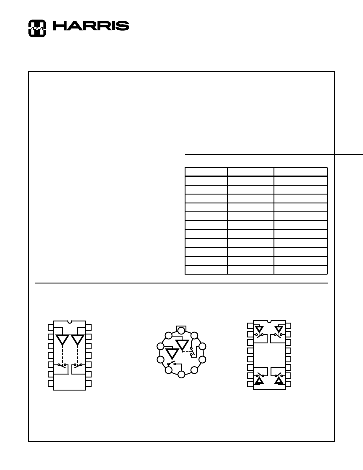
Pinouts
DG200
(CDIP, PDIP)
TOP VIEW
IN
1
2
NC
2
GND
3
NC
4
S
5
2
D
6
2
V-
7
CAUTION: These devices are sensitive to electrostatic discharge. Users should follow proper I.C. Handling Procedures.
Copyright
© Harris Corporation 1993
14
IN
1
NC
13
V+ (SUBSTRATE)
12
NC
11
S
10
1
D
9
1
V
8
REF
(SUBSTRATE AND CASE)
IN
2
GND
DG200
(TO-100 METAL CAN)
TOP VIEW
V+
IN
2
3
S
10
1
1
4
2
9
6
5
D
2
9-13
IN
S
1
D
8
1
7
V
REF
V-
D
S
V-
GND
S
D
IN
DG201
(CDIP, PDIP)
TOP VIEW
16
1
1
2
1
3
1
4
5
6
4
7
4
8
4
IN
2
15
D
2
14
S
2
13
V+(SUBSTRATE)
V
12
REF
11
S
3
10
D
3
9
IN
3
File Number 3115
Page 2
DG200, DG201
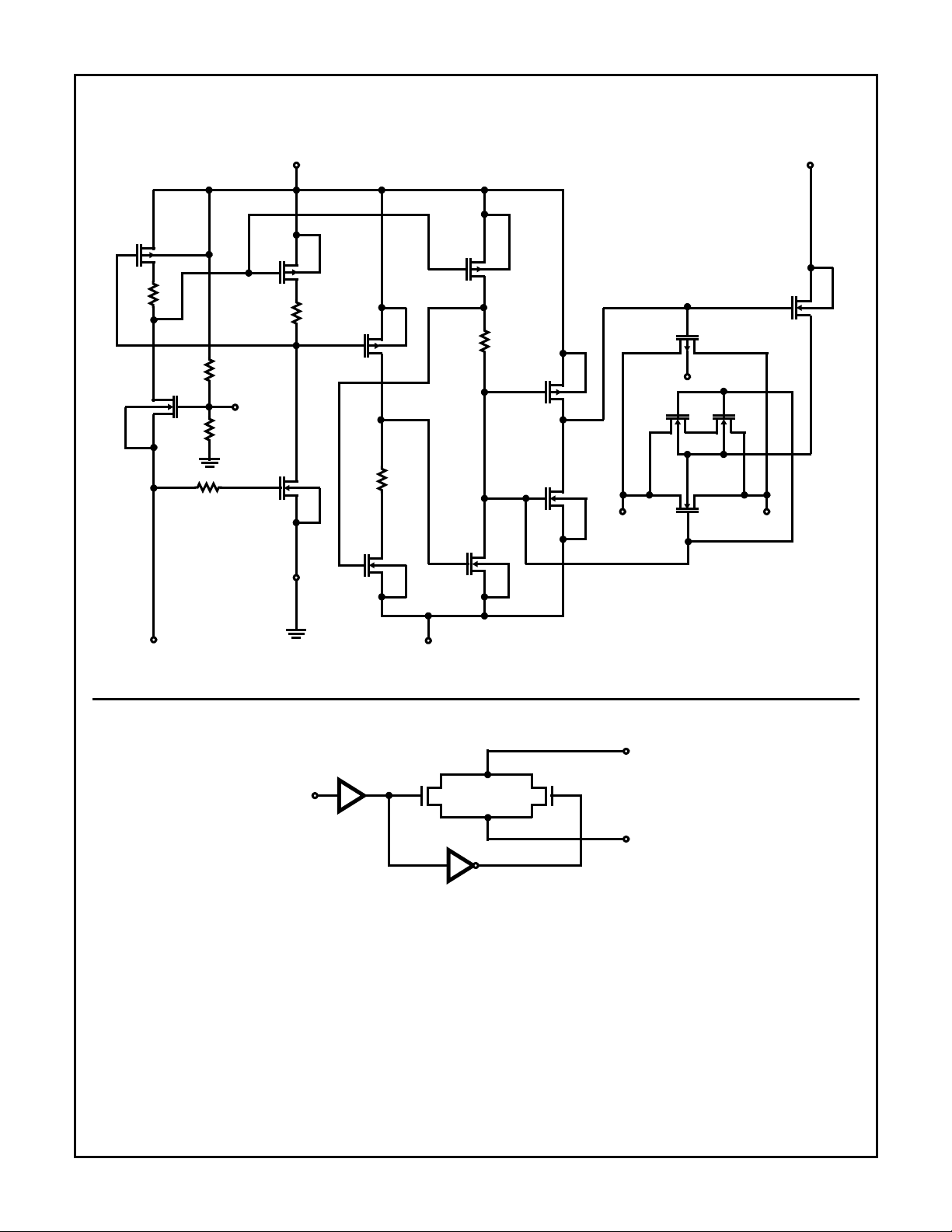
Schematic Diagram
Q3
V
Q1
PROTECTION
RESISTOR
REF
GATE
(1/2 DG200,1/4 DG201)
V+
Q7
Q8
Q2
Q5
Q10
Q9
V-
Q14
Q15
V+
Q12
S
1
Q11
Q13
D
1
INPUT
Functional Diagram
Q4
V-
IN
N
Q6
S
P
D
DG200, DG201 SWITCH CELL
9-14
Page 3
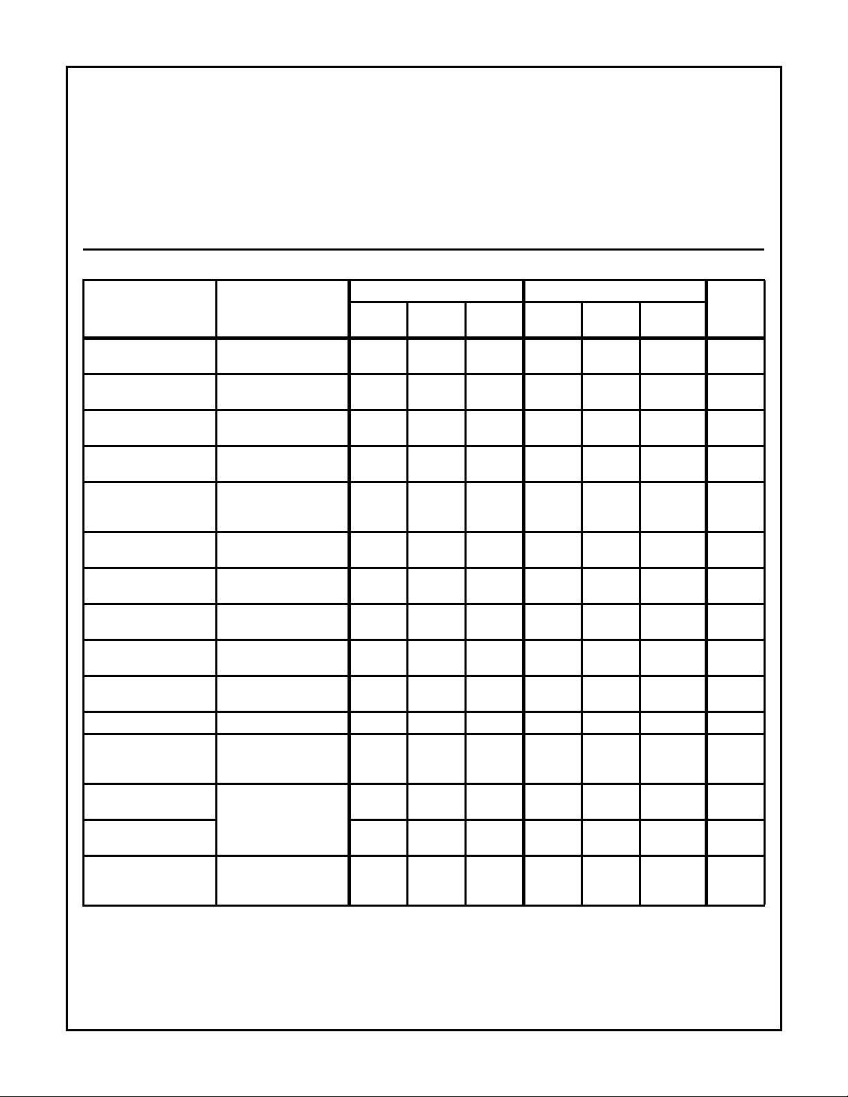
Specifications DG200
Absolute Maximum Ratings Thermal Information
V+, V- . . . . . . . . . . . . . . . . . . . . . . . . . . . . . . . . . . . . . . . . . . . . <36V
V+ - VD. . . . . . . . . . . . . . . . . . . . . . . . . . . . . . . . . . . . . . . . . . . <30V
VD - V- . . . . . . . . . . . . . . . . . . . . . . . . . . . . . . . . . . . . . . . . . . . <30V
VD - VS . . . . . . . . . . . . . . . . . . . . . . . . . . . . . . . . . . . . . . . . . . . <28V
VIN - GND. . . . . . . . . . . . . . . . . . . . . . . . . . . . . . . . . . . . . . . . . <20V
Storage Temperature Range . . . . . . . . . . . . . . . . . -65oC to +150oC
Lead Temperature (Soldering 10s). . . . . . . . . . . . . . . . . . . . +300oC
CAUTION: Stresses above those listed in “Absolute Maximum Ratings” may cause permanent damage to the device. This is a stress only rating and operation
of the device at these or any other conditions above those indicated in the operational sections of this specification is not implied.
Thermal Resistance θ
JA
Ceramic DIP Package. . . . . . . . . . . . . . . 95oC/W 24oC/W
Plastic DIP Package . . . . . . . . . . . . . . . . 100oC/W -
Metal Can Package. . . . . . . . . . . . . . . . . 136oC/W 65oC/W
Operating Temperature Range
“A” Suffix . . . . . . . . . . . . . . . . . . . . . . . . . . . . . . .-55oC to +125oC
“B” Suffix . . . . . . . . . . . . . . . . . . . . . . . . . . . . . . . .-25oC to +85oC
“C” Suffix . . . . . . . . . . . . . . . . . . . . . . . . . . . . . . . . . 0oC to +70oC
θ
JC
Electrical Specifications (T
= +25oC, V+ = +15V, V- = -15V)
A
MILITARY COMMERCIAL / INDUSTRIAL
PARAMETER TEST CONDITIONS
Input Logic Current,
I
IN(ON)
Input Logic Current,
I
N(OFF)
Drain-Source On Resistance, r
DS(ON)
VIN = 0.8V (Notes 2, 3)
VIN = 2.4V (Notes 2, 3) ±10 ±1 ±10 - ±10 ±10 µA
IS = 10mA, V
±10V
Channel-to-Channel
r
Match, r
DS(ON)
DS(ON)
Minimum Analog Signal
ANALOG
o
C +25oC +125oC
10
±
=
70 70 100 80 80 100 Ω
±1 ±10 - ±10 ±10 µA
0oC TO
-25oC +25oC
- 25 (Typ) - - 30 (Typ) - Ω
- ±15V - - ±15V - V
+70oC TO
+85oC
UNITS-55
Handling Capability,
V
ANALOG
Switch OFF Leakage
Current, I
D(OFF)
Switch OFF Leakage
Current, I
S(OFF)
Switch ON Leakage Current, I
D(ON)
+ I
S(ON)
Switch “ON” Time
(Note 1), t
ON
Switch “OFF” Time, t
V
V
= -14V to +14V - ±2 100 -
ANALOG
= -14V to +14V - ±2 100 - ±5 100 nA
ANALOG
5
±
100 nA
VD = VS = -14V to +14V - ±2 200 - ±10 200 nA
RL = 1kΩ, V
ANALOG
=
- 1.0 - - 1.0 - µs
-10V to +10V (Figure 5)
OFFRL
= 1kΩ, V
ANALOG
=
- 0.5 - - 0.5 - µs
-10V to +10V (Figure 5)
Charge Injection, Q
Minimum Off Isolation
Rejection Ratio, OIRR
Figure 6 - 15 (Typ) - - 20 (Typ) - mV
(INJ.)
f = 1MHz, RL = 100Ω,
- 54 (Typ) - - 50 (Typ) - dB
CL≤ 5pF
(Figure 7, Note 1)
+Power Supply
Quiescent Current, I
-Power Supply
Quiescent Current, I
Minimum Channel to
VIN = 0V or VIN = 5V 1000 1000 2000 1000 1000 2000 µA
V1
1000 1000 2000 1000 1000 2000 µA
V2
One Channel Off - 54 (Typ) - - 50 (Typ) - dB
Channel Cross Coupling
Rejection Ratio, CCRR
NOTES:
1. Pull Down Resistor must be ≤ 2kΩ.
2. Typical values are for design aid only, not guaranteed and not subject to production testing.
3. All channels are turned off by high “1” logic inputs and all channels are turned on by low “0” inputs; however 0.8V to 2.4V describes the
minimum range for switching properly. Peak input current required for transition is typically -120µA.
9-15
Page 4
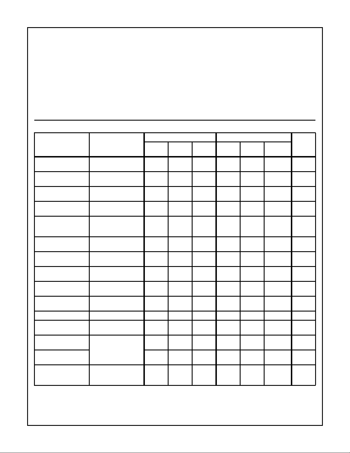
Specifications DG201
Absolute Maximum Ratings Thermal Information
V+ to V-. . . . . . . . . . . . . . . . . . . . . . . . . . . . . . . . . . . . . . . . . . . <36V
V+ to VD. . . . . . . . . . . . . . . . . . . . . . . . . . . . . . . . . . . . . . . . . . <30V
VD to V- . . . . . . . . . . . . . . . . . . . . . . . . . . . . . . . . . . . . . . . . . . <30V
VD to VS. . . . . . . . . . . . . . . . . . . . . . . . . . . . . . . . . . . . . . . . . . <28V
V
to V-. . . . . . . . . . . . . . . . . . . . . . . . . . . . . . . . . . . . . . . . . <33V
REF
V
to VIN. . . . . . . . . . . . . . . . . . . . . . . . . . . . . . . . . . . . . . . . <30V
REF
V
to GND . . . . . . . . . . . . . . . . . . . . . . . . . . . . . . . . . . . . . . <20V
REF
VIN to GND. . . . . . . . . . . . . . . . . . . . . . . . . . . . . . . . . . . . . . . . <20V
Current (Any Terminal) . . . . . . . . . . . . . . . . . . . . . . . . . . . . . .<30mA
Storage Temperature Range . . . . . . . . . . . . . . . . . -65oC to +150oC
Lead Temperature (Soldering 10s). . . . . . . . . . . . . . . . . . . . +300oC
CAUTION: Stresses above those listed in “Absolute Maximum Ratings” may cause permanent damage to the device. This is a stress only rating and operation
of the device at these or any other conditions above those indicated in the operational sections of this specification is not implied.
Thermal Resistance θ
JA
Ceramic DIP Package. . . . . . . . . . . . . . . 80oC/W 24oC/W
Plastic DIP Package . . . . . . . . . . . . . . . . 145oC/W -
Operating Temperature Range
“A” Suffix . . . . . . . . . . . . . . . . . . . . . . . . . . . . . . .-55oC to +125oC
“B” Suffix . . . . . . . . . . . . . . . . . . . . . . . . . . . . . . . .-25oC to +85oC
“C” Suffix . . . . . . . . . . . . . . . . . . . . . . . . . . . . . . . . . 0oC to +70oC
θ
JC
Electrical Specifications (T
= +25oC, V+ = +15V, V- = -15V)
A
MILITARY COMMERCIAL / INDUSTRIAL
PARAMETER TEST CONDITIONS
Input Logic Current,
I
IN(ON)
Input Logic Current,
I
N(OFF)
Drain-Source On Resistance, r
DS(ON)
VIN = 0.8V (Note 1)
VIN = 2.4V (Note 1) 10 ±110±1±110µA
IS = 10mA, V
±10V
Channel-to-Channel
r
Match, r
DS(ON)
DS(ON)
Minimum Analog Signal
ANALOG
o
C +25oC +125oC
10
=
80 80 125 100 100 125 Ω
±110±1±110µA
0oC TO
-25oC +25oC
- 25 (Typ) - - 30 (Typ) - Ω
- ±15 (Typ) - - ±15 (Typ) - V
+70oC TO
+85oC
UNITS-55
Handling Capability,
V
ANALOG
Switch OFF Leakage
Current, I
D(OFF)
Switch OFF Leakage
Current, I
S(OFF)
Switch ON Leakage Current, I
D(ON)
+ I
S(ON)
Switch “ON” Time
(Note 2), t
ON
Switch “OFF” Time
(Note 2), t
OFF
Charge Injection, Q
Minimum Off Isolation
Rejection Ratio, OIRR
+Power Supply
Quiescent Current, I+
-Power Supply
Quiescent Current, IMinimum Channel to
V
V
= -14V to +14V - ±1 100 -
ANALOG
= -14V to +14V - ±1 100 - ±5 100 nA
ANALOG
5
±
VD = VS = -14V to +14V - ±2 200 - ±5 200 nA
RL = 1kΩ, V
ANALOG
=
- 1.0 - - 1.0 - µs
-10V to +10V (Figure 5)
RL = 1kΩ, V
ANALOG
=
- 0.5 - - 0.5 - µs
-10V to +10V (Figure 5)
Figure 6 - 15 (Typ) - - 20 (Typ) - mV
(INJ.)
f = 1MHz, RL = 100Ω,
- 54 (Typ) - - 50 (Typ) - dB
CL≤ 5pF, (Figure 7)
VIN = 0V or VIN = 5V 2000 1000 2000 2000 1000 2000 µA
Q
2000 1000 2000 2000 1000 2000 µA
Q
One Channel Off - 54 (Typ) - - 50 (Typ) - dB
100 nA
Channel Cross Coupling
Rejection Ratio, CCRR
NOTES:
1. Typical values are for design aid only, not guaranteed and not subject to production testing.
2. All channels are turned off by high “1” logic inputs and all channels are turned on by low “0” inputs; however 0.8V to 2.4V describes the
minimum range for switching properly. Peak input current required for transition is typically -120µA.
9-16
Page 5
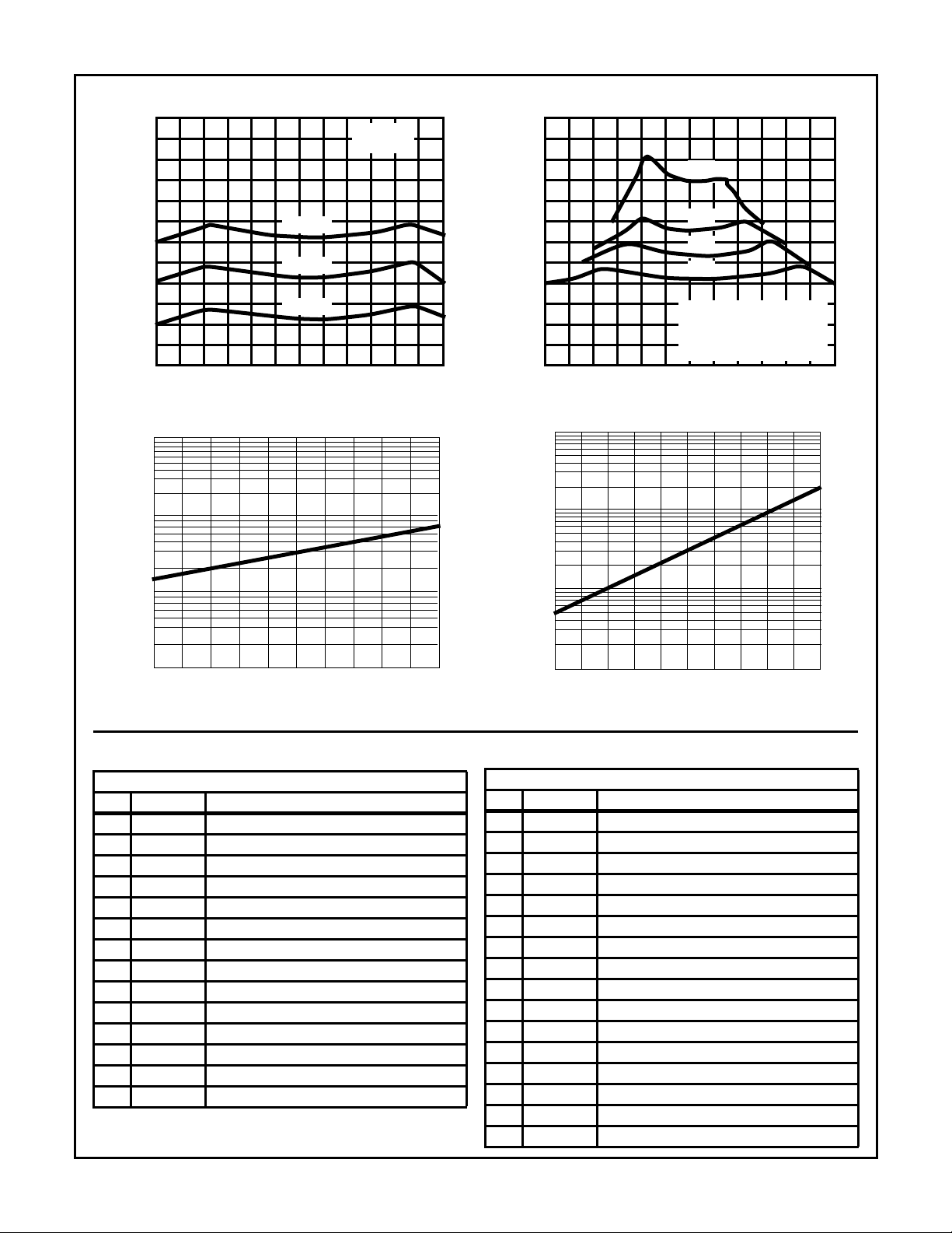
Performance Curves
100
V+ = +15V
V- = -15V
DG200, DG201
100
D
+125oC
50
DRAIN SOURCE ON RESISTANCE (Ω)
0
-15 -10 -5 0 5 10 15
FIGURE 1. R
10
1
0.1
CHANNEL ON LEAKAGE CURRENT (nA)
0.01
25 45 65 85 105 125
DS(ON)
FIGURE 3. I
TEMPERATURE (
D(ON)
+25oC
-55oC
DRAIN VOLTAGE (V)
vs VD AND TEMPERATURE FIGURE 2. r
o
C)
vs TEMPERATURE FIGURE 4. I
C
B
50
DRAIN SOURCE ON RESISTANCE (Ω)
0
-15 -10 -5 0 5 10 15
DS(ON)
10
1
0.1
0.01
25 45 65 85 105 125
SOURCE OR DRAIN OFF LEAKAGE CURRENT (nA)
DRAIN VOLTAGE (V)
vs VD AND POWER SUPPLY VOLTAGE
TEMPERATURE (
OR I
S(OFF)
A
A: V+ = +15V, V- = -15V
B: V+ = +12V, V- = -12V
C: V+ = +10V, V- = -10V
D: V+ = +8V, V- = -8V
o
C)
vs TEMPERATURE
D(OFF)
Pin Description
DG200 (14 LEAD DIP)
PIN SYMBOL DESCRIPTION
1IN
2 NC No Connection
3 GND Ground Terminal (Logic Common)
4 NC No Connection
5S
6D
7 V- Negative power supply terminal
8V
REF
9D
10 S
11 NC No Connection
12 V+ Positive power supply terminal (substrate)
13 NC No Connection
14 IN
Logic control for switch 2
2
Source (input) terminal for switch 2
2
Drain (output) terminal for switch 2
2
Logic reference voltage
Drain (output) terminal for switch 1
1
Source (input) terminal for switch 1
1
Source (input) terminal for switch 1
1
DG201 (16 LEAD DIP)
PIN SYMBOL DESCRIPTION
1IN
2D
3S
Logic control for switch 1
1
Drain (output) terminal for switch 1
1
Source (input) terminal for switch 1
1
4 V- Negative power supply terminal
5 GND Ground terminal (Logic Common)
6S
7D
8IN
9IN
10 D
11 S
12 V
REF
Source (input) terminal for switch 4
4
Drain (output) terminal for switch 4
4
Logic control for switch 4
4
Logic control for switch 3
3
Drain (output) terminal for switch 3
3
Source (input) terminal for switch 3
3
Logic reference voltage
13 V+ Positive power supply terminal (substrate)
14 S
15 D
16 IN
Source (input) terminal for switch 2
2
Drain (output) terminal for switch 2
2
Logic control for switch 2
2
9-17
Page 6
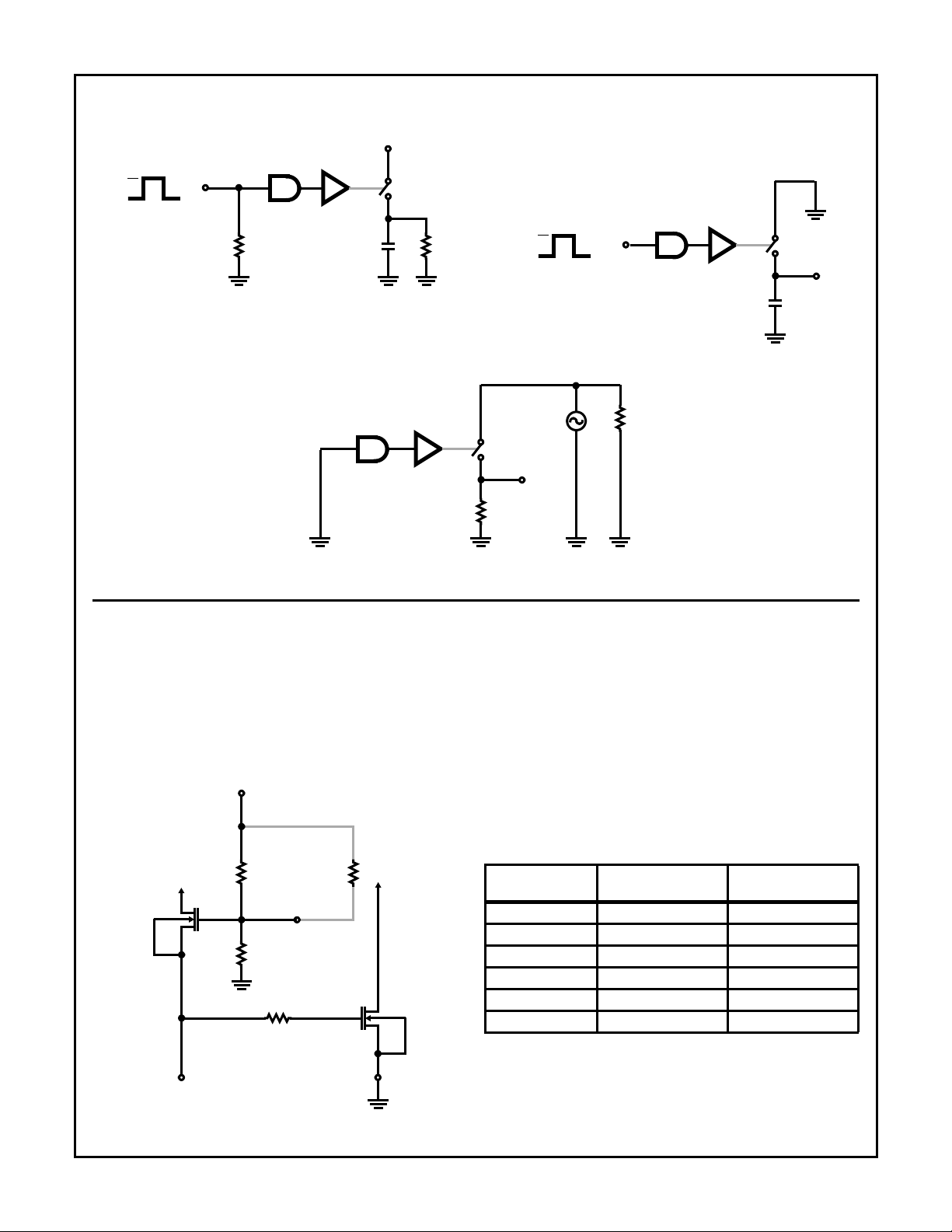
Test Circuits
ANALOG
INPUT 10V
3V
0V
LOGIC
INPUT
≤2kΩ
NOTE: All channels are turned off by high “1” logic inputs and
all channels are turned on by low “0” inputs; however 0.8V to
2.4V describes the minimum range for switching properly.
Peak input current required for transition is typically -120
FIGURE 5. FIGURE 6.
LOGIC
INPUT *
10pF
DG200, DG201
V
OUT
2V
3V
0V
AT 1MHz
P-P
1kΩ
µA.
V
LOGIC
INPUT
OUT
51Ω
INPUT 10V
10,000pF
ANALOG
V
OUT
* Pull Down Resistor must be ≤ 2kΩ.
FIGURE 7.
Typical Applications
Using the V
The DG200 and DG201 have an internal voltage divider setting the TTL threshold on the input control lines for V+ equal
to +15V. The schematic shown in Figure 8 with nominal
resistor values, gives approximately 2.4V on the V
As the TTL input signal goes from +0.8V to +2.4V, Q1 and
Q2 switch states to turn the switch ON and OFF.
REF
Q1
Terminal
V+ (+15V)
31k
Ω
V
REF
6kΩ
GATE
PROTECTION
RESISTOR
pin.
REF
R
EXT
Q2
100Ω
If the power supply voltage is less than +15V, then a resistor
must be added between V+ and the V
+2.4V at V
. The table shows the value of this resistor for
REF
pin, to restore
REF
various supply voltages, to maintain TTL compatibility. If
CMOS logic levels on a +5V supply are being used, the
threshold shifts are less critical, but a separate column of
suitable values is given in the table. For logic swings of -5V
to + 5V, no resistor is needed.
In general, the “low” logic level should be <0.8V to prevent
Q1 and Q2 from both being ON together (this will cause
incorrect switch function).
TABLE 1.
TTL RESISTOR
V+ SUPPLY (V)
(kΩ)
+15 - +12 100 +10 51 -
+9 (34) 34
+8 (27) 27
+7 18 18
CMOS RESISTOR
(kΩ)
INPUT
FIGURE 8.
9-18
Page 7
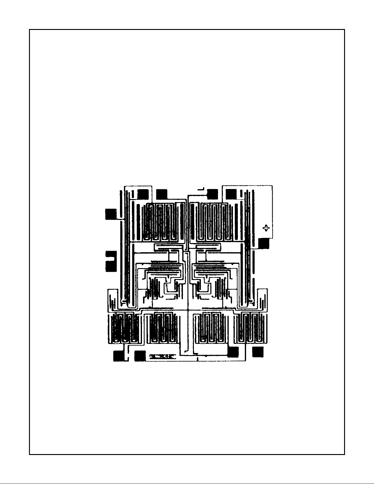
Metallization Topology
DIE DIMENSIONS:
74 x 77 x 14 ± 1mils
METALLIZATION:
Type: Al
Thickness: 10k
Å ± 1kÅ
GLASSIVATION:
Type: SiO
/Si3N
2
4
SiO2 Thickness: 7kÅ ± 1.4kÅ
Si3N4 Thickness: 8kÅ ± 1.2kÅ
WORST CASE CURRENT DENSITY:
1 x 10
5
A/cm
2
Metallization Mask Layout
DG200
DG200
S1 (10)
V- (SUBSTRATE)* (12)
D
(9)
(6)
D
2
(5) S
2
1
V-
(7)
* Backside of Chip is V+
(14)
IN
(1)
IN
1
2
(3)
GND
9-19
Page 8
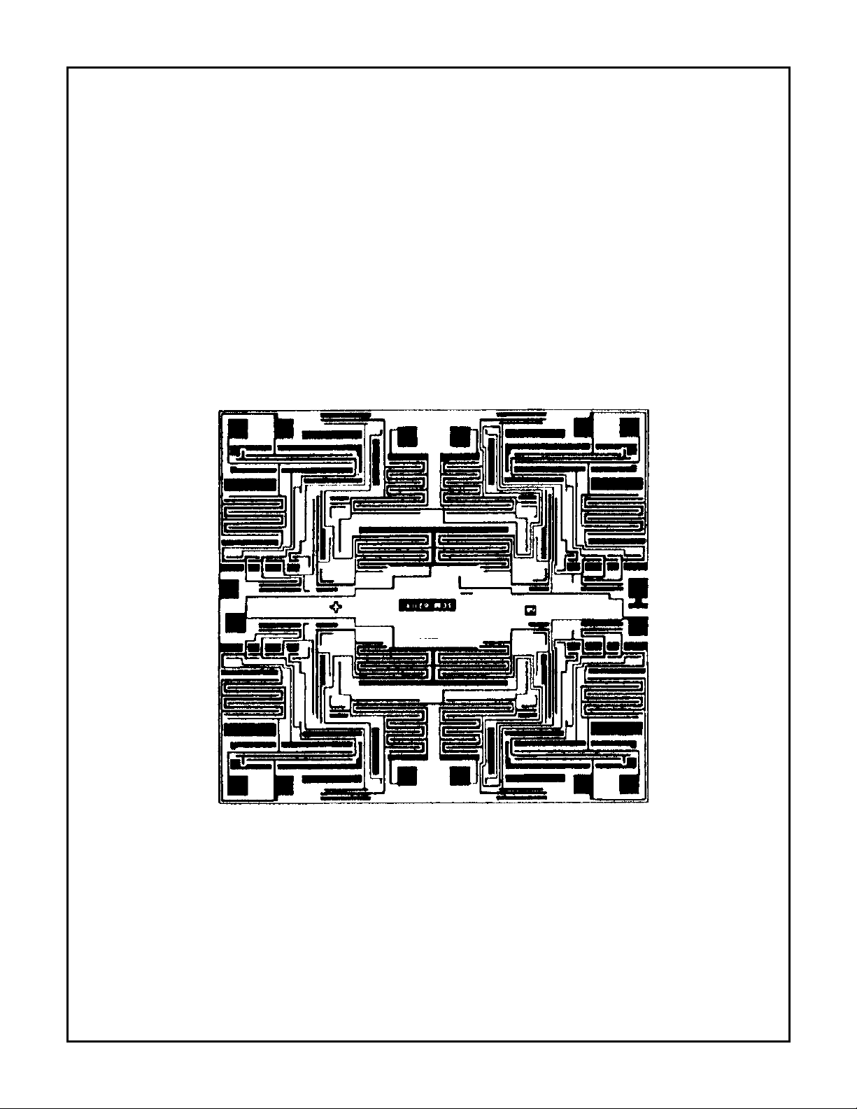
Metallization Topology
DIE DIMENSIONS:
94 x 101 x 14 ± 1mils
METALLIZATION:
Type: Al
Thickness: 10k
Å ± 1kÅ
GLASSIVATION:
Type: SiO
/Si3N
2
4
SiO2 Thickness: 7kÅ ± 1.4kÅ
Si3N4 Thickness: 8kÅ ± 1.2kÅ
WORST CASE CURRENT DENSITY:
1 x 10
5
A/cm
2
Metallization Mask Layout
DG201
DG201
S1 (3)
V- (4)
GND (5)
(6)
S
4
D
(2)
IN
1
1
(1)
IN
(16)
2
D
(15)
2
(14) S
2
(13) V+ (SUBSTRATE)*
(11) S
3
(7)
(8)
D
4
IN
4
(9)
IN
3
(10)
D
3
* Backside of Chip is V+
9-20
 Loading...