

Page 1
DISPLAY Elektronik GmbH
LCD MODULE
DEM 128064A SYH-LY
Product Specification
Version: 10.1.3
31.07.2008
Page 2
GENERAL SPECIFICATION
MODULE NO. :
DEM 128064A SYH-LY
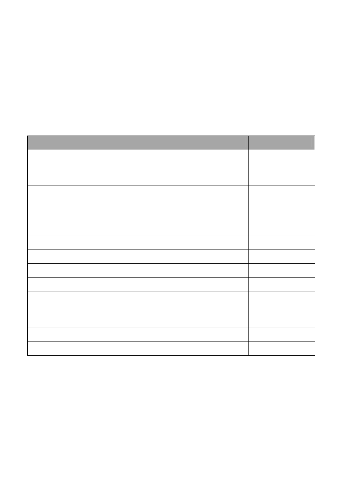
VERSION NO. CHANGE DESCRIPTION DATE
0 ORIGINAL VERSION 30.05.2002
1
2
3 ADD DC/DC CONVERTER 06.07.2002
4 THE PCB CHANGED 12.12.2002
5 CHANGE PCB AND COMPONENT 18.02.2003
6 CHANGE PCB PRINT 17.03.2003
7 ADDING VERSION 07.08.2003
8 ADDING VERSION 03.02.2005
9
10 ADDING VERSION 03.11.2005
10.1.3 CHANGE IC 31.07.2008
EXTERNAL DIMENSIONS
30.05.2002
CHANGED
LCD TYPE AND EXTERNAL
03.06.2002
DIMENSIONS CHANGED
CHANGED FUNCTIONS &
24.02.2005
FEATURES
PREPARED BY: HCL DATE: 31.07.2008
APPROVED BY: MH DATE: 31.07.2008
Page 3

DEM 128064A SYH-LY Product Specification
CONTENTS
1. FUNCTIONS & FEATURES ....................................................................................................................................................2
2. MECHANICAL SPECIFICATIONS........................................................................................................................................2
3. EXTERNAL DIMENSIONS......................................................................................................................................................3
4. BLOCK DIAGRAM................................................................................................................................................................... 4
5.PIN ASSIGNMENT.....................................................................................................................................................................4
6.0 PCB DRAWING AND DESCRIPTION..................................................................................................................................5
6.1 EXAMPLE APPLICATION....................................................................................................................................................5
7. BACKLIGHT & SWITCH........................................................................................................................................................6
8. APPLICA TION CIRCUIT.........................................................................................................................................................7
9. MAXIMUM ABSOLUTE POWER RATINGS .......................................................................................................................7
10. ELECTRICAL CHARACTERISTICS ..................................................................................................................................8
11. OPERATING PRINCIPLES & METHODS........................................................................................................................10
12. DISPLAY CONTROL INSTRUCTION...............................................................................................................................13
13. LCD MODULES HANDLING PRECAUTIONS................................................................................................................15
14. OTHERS .................................................................................................................................................................................15
Version: 10.1.3 PAGE: 1
Page 4

DEM 128064A SYH-LY Product Specification
1. FUNCTIONS & FEATURES
MODULE NAME LCD T ype
DEM 128064A SYH-LY STN Yellow Green Transflective Positive Mode
z Viewing Direction : 6 o’clock
z Driving Scheme : 1/64 Duty Cycle, 1/9 Bias
z Power Supply Voltage : 5.0 V (typ.)
z VLCD (VDD –V5) : 12.9 V (typ.)
z Backlight Color : LED, Lightbox, Yellow Green
z Display Contents : 128 x 64 Dots
z Interface RAM : 512 bytes (4096 bits)
z Interface : 8 bit parallel display data from MPU
z Operating Temperature : - 20°C to + 70°C
z Storage Temperature : - 25°C to + 75°C
2. MECHANICAL SPECIFICATIONS
z Module Size : 93.00 x 70.00 x 13.00 mm
z Module Size : 93.00 x 70.00 x 10.20 mm
z Dot Size : 0.48 x 0.48 mm
z Dot Pitch : 0.52 x 0.52 mm
z Dot Gap : 0.04 mm
Version: 10.1.3 PAGE: 2
Page 5
DEM 128064A SYH-LY Product Specification
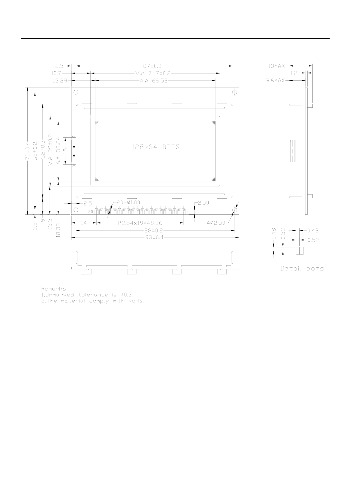
3. EXTERNAL DIMENSIONS
Version: 10.1.3 PAGE: 3
Page 6
DEM 128064A SYH-LY Product Specification
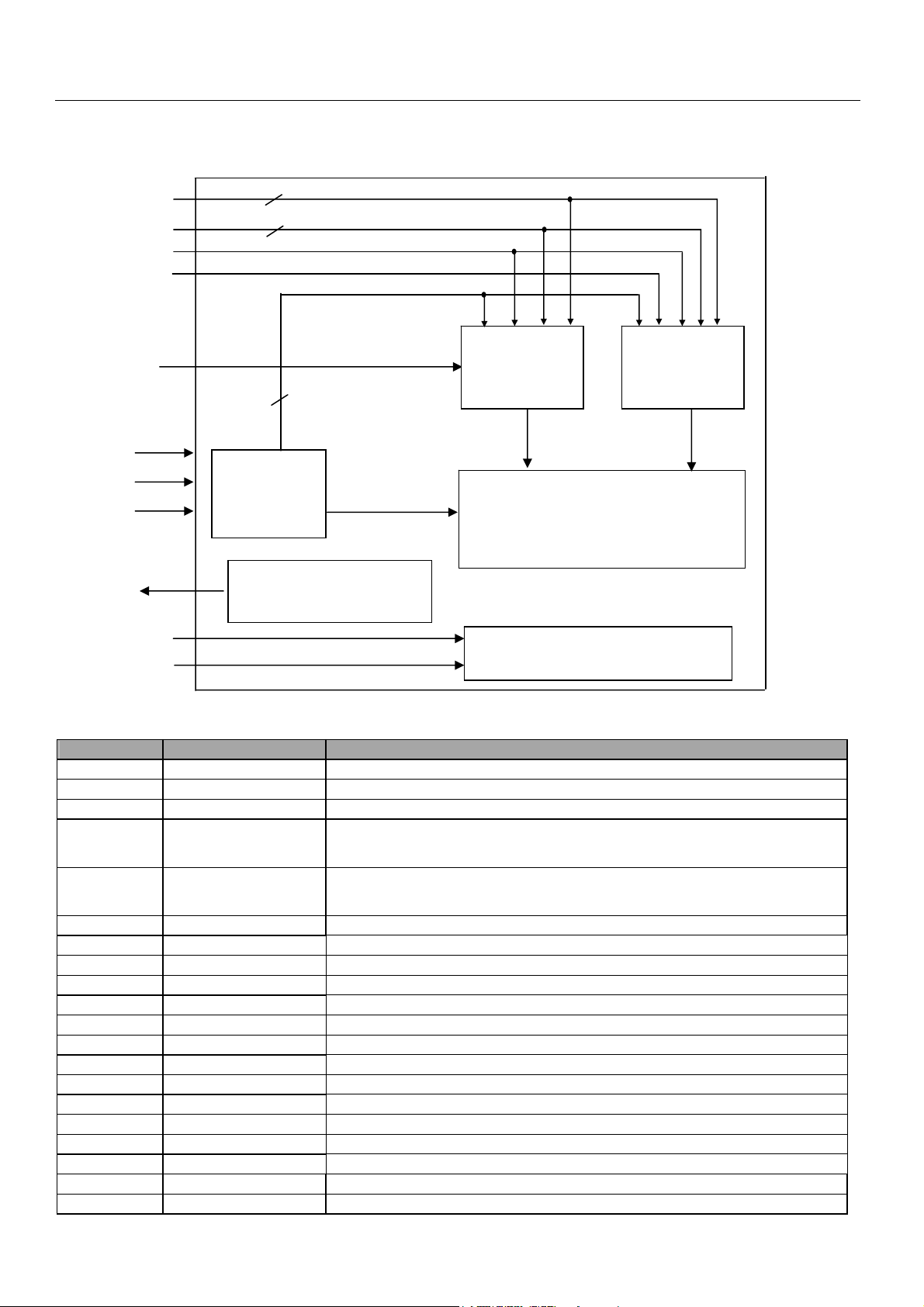
4. BLOCK DIAGRAM
DB0~DB7
RS, R/W, E
RSTB
CS2
CS1
VSS
VDD
V0
VOUT
LED+(A)
LED-(K)
8
3
5
COMMON
DRIVER IC
SBN6400G
DC/DC Converter
SCI7661M or NJU7670M
Com1~Com64
SEGMENT
DRIVER IC
SBN0064G
Seg1~Seg64
LED BACK LIGHT
SEGMENT
DRIVER IC
SBN0064B
Seg65~Seg128
LCD PANEL
128 × 64 DOTS
5.PIN ASSIGNMENT
Pin No. Symbol Function
1 VSS Ground
2 VDD Power supply voltage for logic,+ 5.0V.
3 V0 Input voltage for LCD
4 RS
5 R/W
6 E Chip enable signal
7 DB0 Data bit 0
8 DB1 Data bit 1
9 DB2 Data bit 2
10 DB3 Data bit 3
11 DB4 Data bit 4
12 DB5 Data bit 5
13 DB6 Data bit 6
14 DB7 Data bit 7
15 CS1 Chip select signal for SBN0064G(1)
16 CS2 Chip select signal for SBN0064G(2)
17 RSTB Reset signal
18 VOUT Output voltage for LCD,-9.5V
19 LED + (A) Please also refer to 6.2 Example application
20 LED – (K) Please also refer to 6.2 Example application
Register select
RS = 0…Instruction register RS = 1…Data register
Read /Write
R/W = 1…Read R/W = 0…Write
Version: 10.1.3 PAGE: 4
Page 7
DEM 128064A SYH-LY Product Specification
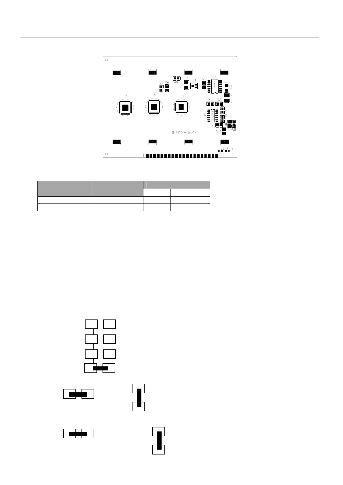
6.0 PCB DRAWING AND DESCRIPTION
DESCRIPTION:
6-0-1.The polarity of the pin 19 and the pin 20:
J2,J4 J1, J3
Each open Each close Anode Cathode
Each close Each open Cathode Anode
Note: In application module, J1=J3=0 Ohm, J2=J4=open.
6-0-2.The LED resistor should be bridged when the J5 is solder-Bridge.
Note: In application module, J5=open
6-0-3.The R8, R9 and R10 are the LED resistor.
Note: In application module, R8=R9=R10=8.2 ohm
6-0-4. The metal-bezel should be on ground when the J6 is solder-Bridge.
Note: In application module, J6=0 Ohm
6-0-5.The mounting holes should be on ground ,when the J7 is solder-bridge.
Note: In application module,J7=0 Ohm
LED Polarity
19 Pin 20 Pin
6. 1 Example application
6-1-1. The LED resistor should be bridged as following.
6-1-2. The 19 pin is the anode and the 20 pin is the cathode as following.
6-1-3.The 19 pin is the cathode and the 20 pin is the anode as following.
J1
J2
Version: 10.1.3 PAGE: 5
R10
R9
R8
J5
J3
J4
Page 8
DEM 128064A SYH-LY Product Specification
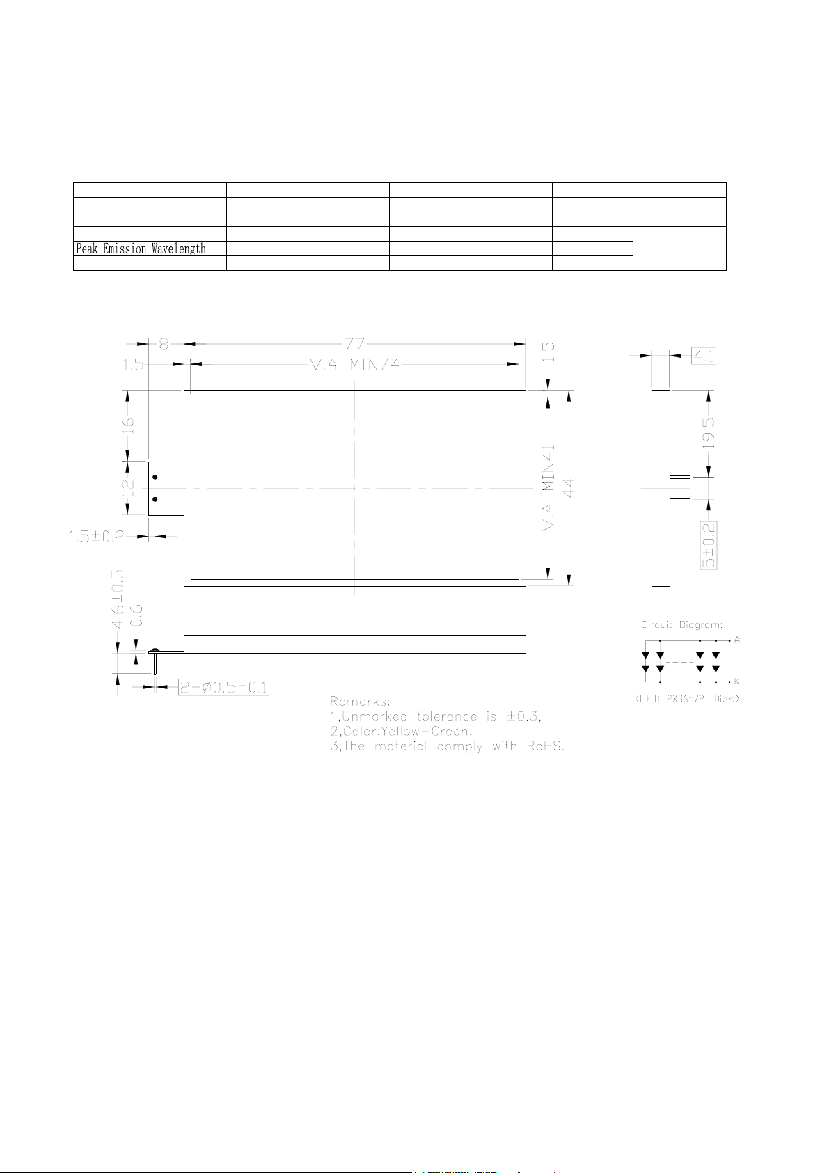
7. BACKLIGHT & SWITCH (Ta=-20~+70°C)
El ect r i cal / Opt i cal Speci f i cat i ons( Ta=25 ° C) :
ITEM
For war d Vol t age
Re v e r s e Cu r r e n t
SYMBOLUNIT
Vf
MIN.
3. 8 4. 2
If
TYP.
4. 0
MAX.
0. 1
Rever se Vol t age Vr 5. 0 V
λP
569 572 575 nm
163
204
A
K
CONDITIONS
V
I f =360mA
mA
I f =360mA
2
cd/ m LvLuminous Intensity
Version: 10.1.3 PAGE: 6
Page 9
DEM 128064A SYH-LY Product Specification
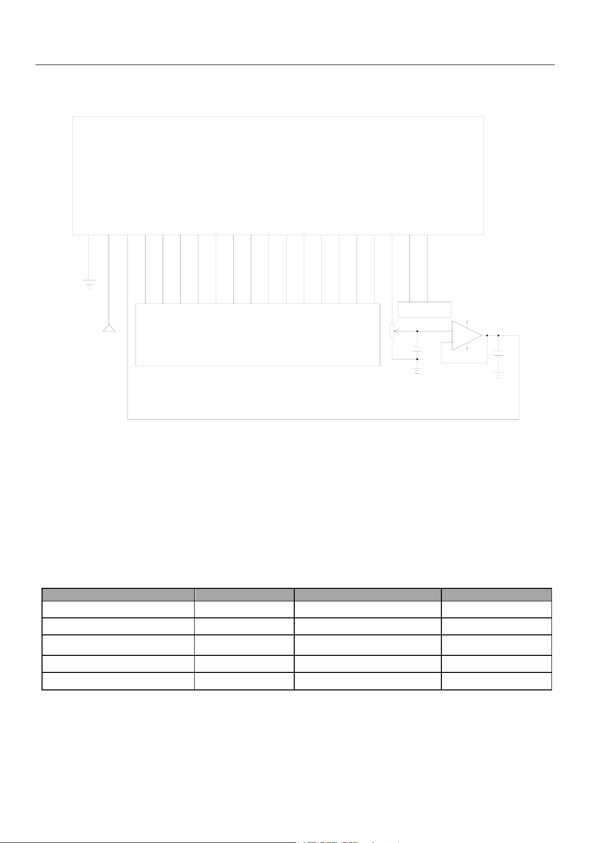
8. APPLICA TION CIRCUIT
LCD Module
128 X 64 dots
VSS
VDD
V0
RS
R/WEDB0
DB1
DB2
DB3
DB4
DB5
DB6
DB7
CS1
CS2
VOUT
RSTB
LED+(A)
LED-(K)
1
2
+5.0V
NOTE: 1. R1 is the contrast resistor.
2. VOUT=-9.5V
3. Adjust R1, it will be best contrast when V0 is –7.9V.
4
3
5
7
6
9
8
111213
10
MCU
141516
17
18
19
LED CONTROL
R1
10K
+
C1
20
V+
U1
LM324
+
V-
+
C2
9. MAXIMUM ABSOLUTE POWER RATINGS ( Ta=25°C)
Item Symbol Standard value Unit
Supply voltage for logic VDD -0.3~+7.0 V
Supply voltage V0 V
Driver supply voltage V
Operating temperature Topr -20~+70 °C
Storage temperature Tstg -25~+75 °C
LCD(VDD
–V5) V0 -0.3~VDD+0.3 V
Version: 10.1.3 PAGE: 7
-19.0~VDD+0.3 V
DD
Page 10
DEM 128064A SYH-LY Product Specification
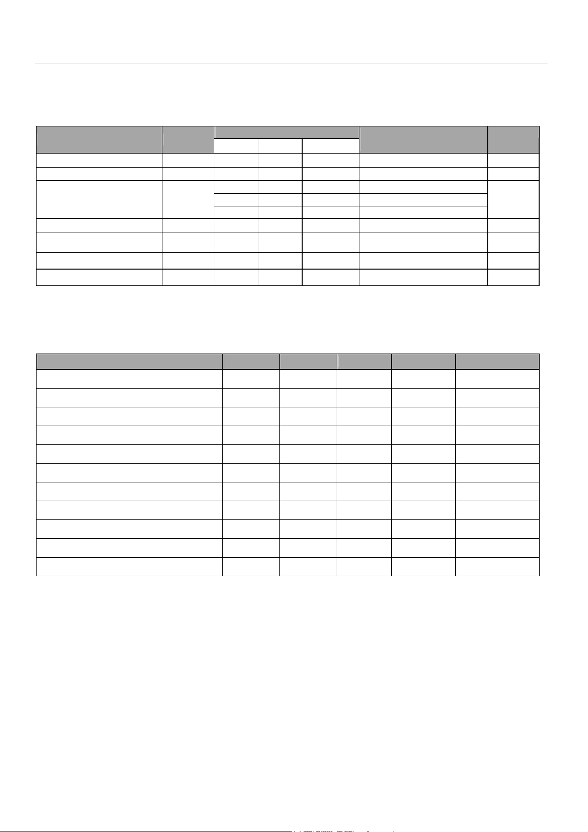
10. ELECTRICAL CHARACTERISTICS
10-1 DC Characteristics (VDD=+5±10% Vss=0V, Ta=-20~+70°C)
Item Symbol
Supply current for logic V
Supply current for logic I
operating Voltage for LCD VDD-V
Supply voltage for back light V
Supply current back light I
DD
DD
5
F
F
Input voltage “H” level VIH 0.7V
Input voltage “L” level VIL 0 --- 0.3V
Standard Value
MIN TYP MAX
4.5 5.0 5.5 ------- V
---- 2.62 4 ------- mA
13.4 14.1 14.8 -20°C
12.2 12.9 13.6
11.0 11.7 12.4 70°C
--- 4.2 4.6 ---------- V
--- 380 500 VF=4.2V mA
DD
--- V
DD
DD
10-2 AC Characteristics
Characteristic Symbol Min Typ Max Unit
E Cycle t
C
1000
-
Test
Condition
25°C
--- V
--- V
- ns
Unit
V
E Rise t
E Fall t
E High Level Width t
E-Low Level Width t
Address Set –Up Time t
Address Hold Time t
Data Delay Time t
Data Set –Up Time t
Data Hold Time ( Write) t
Data Hold Time (Read) t
R
F
WH
WL
ASU
AH
D
DSU
DHW
DHR
-
-
450
450
140
10
-
200
10
20
-
-
-
25 ns
25 ns
- ns
- -
- -
- -
-
320 ns
- -
- -
- -
ns
ns
ns
ns
ns
ns
Version: 10.1.3 PAGE: 8
Page 11
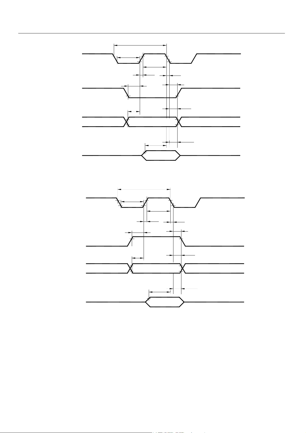
DEM 128064A SYH-LY Product Specification
tC
E
R/W
CS1,CS2
DB0~DB7
0.8V
tWL
tASU
tASU
tWH
tR
tDSU
tF
tAH
tAH
2.0V
tDHW
2.0V
0.8V
Figure 5.0 MPU write timing
tC
E
tWL
tWH
tR
tASU
R/W
tASU
CS1,CS2
tD
DB0~DB7
tF
tAH
tAH
tDHR
Figure 6.0 MPU Read timing
Version: 10.1.3 PAGE: 9
Page 12
DEM 128064A SYH-LY Product Specification
11. OPERATING PRINCIPLES & METHODS
11-1. I/O Buffer
Input buffer controls the status between the enable the and disable of chip. Unless the CS1 to CS2 is in active mode. Input
or output of data and instruction does not execute. Therefore internal stade is not change.
Bust RSTB and ADC can operate regardless CS1-CS2.
11-2. Input register
Input register is provided to interface with MPU which is different operating frequency. Input register stores the data
temporarily before writing it into display RAM. When CS1 to CS2 are in the active mode, R/W and RS select the input
register. The data from MPU is written into input register. Then Writing it into display RAM. Data latched for the E signal
and write automatically into the display data RAM by internal operation.
11-3. Output register
Output register stores the data temporarily from display data RAM when CS1 and CS2 are in active mode and R/W and
RS=H, stored data in display data RAM is latched in output register. When CS1 to CS2 are in the active mode and R/W=H,
RS=L, status data (busy check) can read out. To read the contents of display data RAM, twice access of read instruction
needed. In first access, data in display data RAM is latched into output register. In second access, MPU can read data
which is latched. That is , to read the data in display data RAM, it needs dummy read. But staus read is not read needed
dummy.
RS R/W
L
H
L
H
L
H
Function
Instruction
Status read (busy check)
Data write (from input read register to display data RAM
Data read (from display data RAM to output register)
11-4. Reset
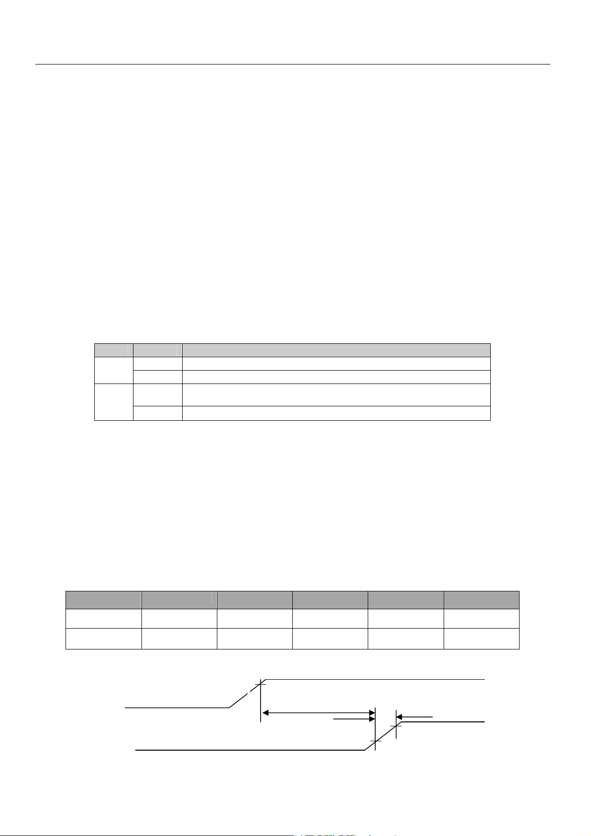
The system can be initialized by setting RSTB terminal at low level when turning power on receiving instruction from
RAM. When RSTB becomes low, following procedure is occurred.
1. Display off
2. Display start line register become set by 0. (Z-address 0)
While RSTB is low, No instruction except status read can be accepted. Therefore, execute other instructions after making
sure than DB4=0 (clear RSTB) and DB7=0 (ready) by status read instruction.
The conditions of power supply data initial power up are shown in table 1.
Table 1. Power Supply Initial Conditions
Item Symb Min. Typ. Max. Unit
Reset time TRS 1
Rise time tR
- -
- -
200 us
us
4.5[V]
V
DD
t
RS
tR
RSTB
0.7VDD
0.3VDD
Figure 7.0
Version: 10.1.3 PAGE: 10
Page 13
DEM 128064A SYH-LY Product Specification
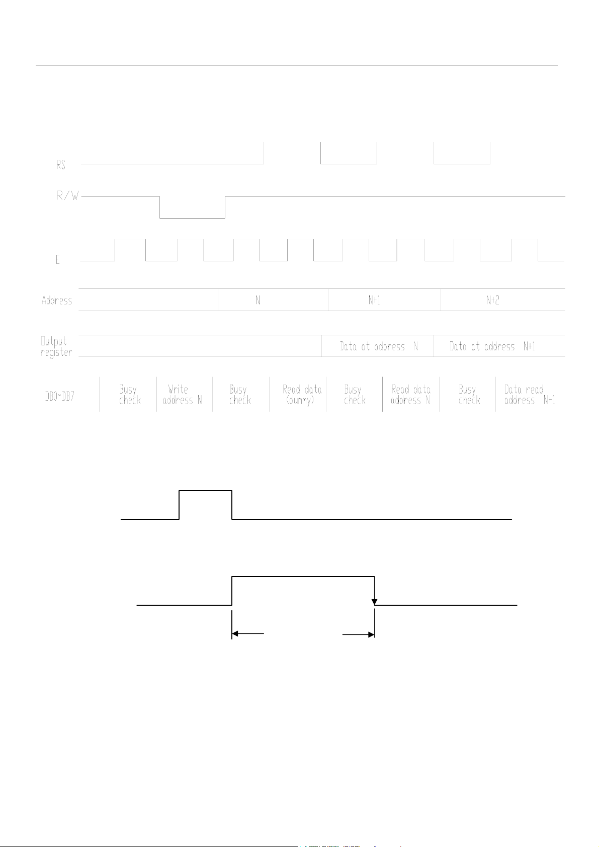
11-5. Busy flag
Busy flag indicates that SBN0064G is operating or on operating. When busy flag is high, SBN0064G is internal operating.
When busy flag is low, SBN0064G can accept the data or instruction.
DB7 indicates busy flag of the SBN0064G.
Figure 8.0 Busy Check.
E
Busy flag
T Busy
Figure
Version: 10.1.3 PAGE: 11
Page 14

DEM 128064A SYH-LY Product Specification
11 -6. Display ON/OFF Flip-Flop
The display on/off flip-flop makes on/off the liquid crystal display. When flip-flop is reset (logical low).
selective voltage or non selective voltage appears on segment output terminals. When flip-flop is set
(logic high), non selective voltage appears on segment output terminals regardless of display RAM data. The display
on/off flip-flop can changes status by instruction. The display data at all segment disappear while RSTB is low. The
status of the flip-flop is output to DB5 by status read instruction.
11-7. X Page Register
X page register designates pages of the internal display data RAM.
Count function is not available. An adders is set by instruction.
11-8. Y address counter
Y address counter designates address of the internal data RAM. An address is set by instruction and is increased by 1
automatically by read or write operations of display data.
11-9. Display Data RAM
Display Data RAM stores a display data for liquid crystal display. To indicate on state dot matrix of liquid crystal display,
write data 1. The other way , off state, writes 0.
11-10. Display Start Line Register
The display start line register indicates of display data RAM to display top liquid crystal display. Bit data
(DB<0:5>) of the display start line set instruction is latched in display start line register. Latched data is transferred to the
Z address counter while FRM is high, presetting the Z address counter. It is used for scrolling of the liquid crystal display
screen.
Version: 10.1.3 PAGE:12
Page 15
DEM 128064A SYH-LY Product Specification
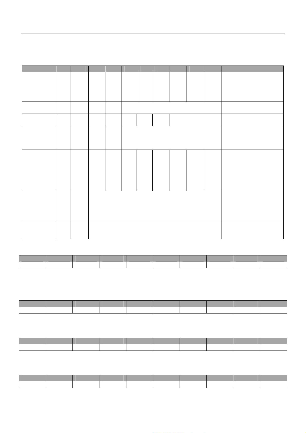
12. DISPLAY CONTROL INSTRUCTION
The display control instructions the internal state of the SBN0064G. Instruction is received from MPU to SBN0064G for
the display control. The following table shows various instructions.
Instruction RS R/W DB7 DB6 DB5 DB4 DB3 DB2 DB1 DB0 Function
Display
ON/OFF
Set Address
(Y address)
Set Page
(X address)
Display Start
line
(Z address)
Status Read L H B
Write Display
Data
Read Display
data
L L L L H H H H L/H Controls the
L L L H Y address (0~63) Sets the Y address
L L H L H H H Page (0~7) Sets the X address
L L H H Display start line (0~63) Indicates the
L O
U
S
Y
H L Write Date Writes data (DB0:7) into
H H Read Date Reads data (DB0:7)
N
/
O
F
F
R
E
S
E
T
12-1. Display On/Off
RS R/W DB7 DB6 DB5 DB4 DB3 DB2 DB1 DB0
0 0 0 0 1 1 1 1 1 D0
The display data appears when D is 1 and disappears when D is 0.
Though the data is not on the screen with D=0, it remains display data RAM.
Therefore, you can make it appear by changing D=0 into D=1.
12-2. Set Address (Y Address)
RS R/W DB7 DB6 DB5 DB4 DB3 DB2 DB1 DB0
0 0 0 1 AC5 AC4 AC3 AC2 AC1 AC0
Y address (AC0~AC5) of the display data RAM is set in the Y address counter.
An address is set by instruction and increased by 1 automatically by read or write operations of display data.
12-3. Set Page (X Address)
RS R/W DB7 DB6 DB5 DB4 DB3 DB2 DB1 DB0
0 0 1 0 1 1 1 AC2 AC1 AC0
X address (AC0~AC2) of the display data RAM is set in the X address register.
Writing or reading to or from MPU is executed in this specified page until the next page is set.
12-4. Display Start Line (Z Address)
RS R/W DB7 DB6 DB5 DB4 DB3 DB2 DB1 DB0
0 0 1 1 AC5 AC4 AC3 AC2 AC1 AC0
Z address (AC0~AC5) of the display data RAM is set in the display start line register and display at the top of the screen.
When the display duty cycle is 1/64 or others (1/32~1/64), the data of total line number of LCD screen, from the line
display on or off. Internal
status and display RAM
data is not affected.
L: OFF, H: ON
in the Y address counter.
At the X address counter
display data RAM
displayed at the top of the
screen.
L L L L Read status
BUSY L: Ready
H: In operation
On/Off L: display ON
H: Display OFF
RESET L: Normal
H: Reset
display data RAM . After
writing instruction, Y
address is increased by 1
automatically.
From display data RAM to
the data bus.
Version: 10.1.3 PAGE: 13
Page 16
DEM 128064A SYH-LY Product Specification
specified by display start line instruction, is displayed.
12-5. Status Read
RS R/W DB7 DB6 DB5 DB4 DB3 DB2 DB1 DB0
0 0 BUSY 0 ON/OFF RESET 0 0 0 0
BUSY
When BUSY is 1, the Chip is executing internal operation and no instructions are accepted.
When BUSY is 0, the Chip is ready to accept any instructions.
ON/OFF
When ON/OFF is 1, the display is on.
When ON/OFF is 0, the display is off.
RESET
When RESET is 1, the system is being initialized.
In this condition is 0, no instructions except status read can be accepted.
When RESET is 0, initialized has finished and the system is in the usual operation condition
12-6. Write Display data
R/W DB7 DB6 DB5 DB4 DB3 DB2 DB1 DB0
1 D7 D6 D5 D4 D3 D2 D1 D0
Writes data (D0~D7) into the display data RAM.
After writing instruction, Y addressed is increased 1 automatically.
12-7. Read Display data
R/W DB7 DB6 DB5 DB4 DB3 DB2 DB1 DB0
1 D7 D6 D5 D4 D3 D2 D1 D0
Reads data (D0~D7) from the display data RAM.
After reading instruction, Y addressed is increased 1 automatically.
Version: 10.1.3 PAGE: 14
Page 17

DEM 128064A SYH-LY Product Specification
13. LCD MODULES HANDLING PRECAUTIONS
Please remove the protection foil of polarizer before using.
The display panel is made of glass. Do not subject it to a mechanical shock by dropping it from a high place, etc.
If the display panel is damaged and the liquid crystal substance inside it leaks out, do not get any in your mouth. If
the substance comes into contact with your skin or clothes promptly wash it off using soap and water.
Do not apply excessive force to the display surface or the adjoining areas since this may cause the color tone to
vary.
The polarizer covering the display surface of the LCD module is soft and easily scratched. Handle this
polarizercarefully.
To prevent destruction of the elements by static electricity, be careful to maintain an optimum work environment.
-Be sure to ground the body when handling the LCD module.
-Tools required for assembly, such as soldering irons, must be properly grounded.
-To reduce the amount of static electricity generated, do not conduct assembly and other work under dry conditions.
-The LCD module is coated with a film to protect the display surface. Exercise care when peeling off this protective
film since static electricity may be generated.
Storage precautions
When storing the LCD modules, avoid exposure to direct sunlight or to the light of fluorescent lamps. Keep the
modules in bags designed to prevent static electricity charging under low temperature / normal humidity conditions
(avoid high temperature / high humidity and low temperatures below 0°C). Whenever possible, the LCD modules
should be stored in the same conditions in which they were shipped from our company.
14. OTHERS
Liquid crystals solidify at low temperature (below the storage temperature range) leading to defective orientation of
liquid crystal or the generation of air bubbles (black or white). Air bubbles may also be generated if the module is
subjected to a strong shock at a low temperature.
If the LCD modules have been operating for a long time showing the same display, patterns may remain on the
screen as ghost images and a slight contrast irregularity may also appear. Abnormal operating status can be resumed
to be normal condition by suspending use for some time. It should be noted that this phenomena does not adversely
affect performance reliability.
To minimize the performance degradation of the LCD modules resulting from caused by static electricity, etc.
exercise care to avoid holding the following sections when handling the modules:
- Exposed area of the printed circuit board
- Terminal electrode sectio ns
Version: 10.1.3 PAGE: 15
 Loading...