

Page 1

QUICK START GUIDE FOR DEMONSTRATION CIRCUIT 536
HOT SWAP CONTROLLER WITH MULTIFUNCTION CURRENT CONTROL
DESCRIPTION
LTC4211
Demonstration circuit DC536 is a Hot Swap controller
with multifunction current control featuring the
LTC4211. The DC536 is configured to operate with up to
7A as populated by the factory. Optional component
pads are provided for a higher power pass FET and
sense resistor for operation up to 20A.
The DC536 permits evaluating the LTC4211 during
turn-on and turn-off transients as well as during steady
state conditions.
Design files for this circuit board are available. Call
the LTC factory.
, LTC and Hot Swap are registered trademarks of Linear Technology Corpora-
tion.
Table 1. Performance Summary (TA = 25°C)
PARAMETER CONDITION VALUE
Supply Voltage Rated operating limits 2.5V ≤ VCC ≤ 16.5V
Under Voltage Lockout Transition to operating mode 2.13V ≤ V
ON Pin Threshold Voltage, High 1.23V ≤ V
ON Pin Threshold Voltage, Low 1.20V ≤ V
Gate Pull-Up current Charge Pump On, V
ON Pin Signal Low 130µA ≤ I
Fast Gate Pull-Down Current
Current Limit
Supply Voltage Rated operating limits 2.5V ≤ VCC ≤ 16.5V
• Latched and Circuit Breaker Tripped or in UVLO 50mA
Si4410 and 7m
FDB8030L and 2.5m
0.2V 7.5µA ≤ I
GATE
Ω
SENSE Resistor
Ω
SENSE Resistor
5.7A ≤I
16A ≤ I
CC(UVL)
CC(UVL)
CC(UVL)
GATE
GATE
LIMIT
LIMIT
≤ 2.47V
≤ 1.39V
≤1.26V
≤ 12.5µA
≤ 270µA Normal Gate Pull-Down Current
≤ 8.5A
≤ 24A
2.13V ≤ V
ON Pin Threshold Voltage, High
Gate Pull-Up current
Normal Gate Pull-Down Current ON Pin Signal Low 130µA ≤ I
1.23V ≤ V
1.20V ≤ V
Charge Pump On, V
0.2V 7.5µA ≤ I
GATE
OPERATING PRINCIPLES
The LTC4211 is a low voltage hot swap controller that
has a 2.5V to 16.5V operating range and a 17V absolute
maximum operating voltage for the Vcc pin. This demo
circuit is populated for +5V operation, but it can easily
be re-adjusted for any voltage between 2.5V to 16.5V by
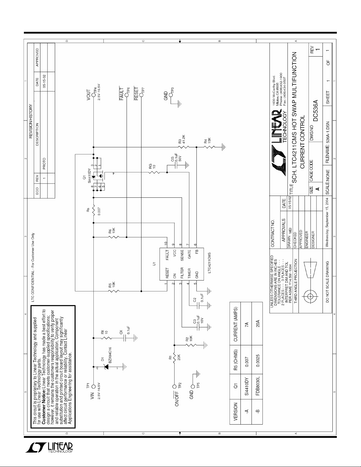
replacing R3 and R1 (top resistors in the feedback divider and the ON pin signal divider). There are two as-
sembly options for load current. The DC536 as supplied
by the factory is populated with an Si4410 MOSFET in an
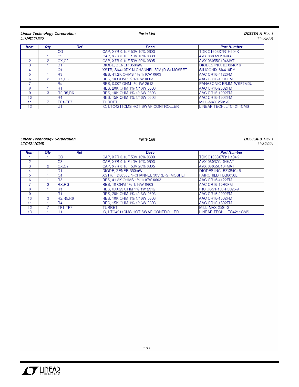
SO-8 package and a 7mΩ current sense resistor providing a minimum 5A load current. The DC536 has provision for an FDB8030L MOSFET in the DD package which
when used with a 2.5mΩ sense resistor provides a
minimum16A load current.
CC(UVL)
CC(UVL)
≤1.26V ON Pin Threshold Voltage, Low
CC(UVL)
≤ 12.5µA
GATE
≤ 270µA
GATE
≤ 2.47V Under Voltage Lockout
≤ 1.39V
1
Page 2

QUICK START GUIDE FOR DEMONSTRATION CIRCUIT 536
HOT SWAP CONTROLLER WITH MULTIFUNCTION CURRENT CONTROL
QUICK START PROCEDURE
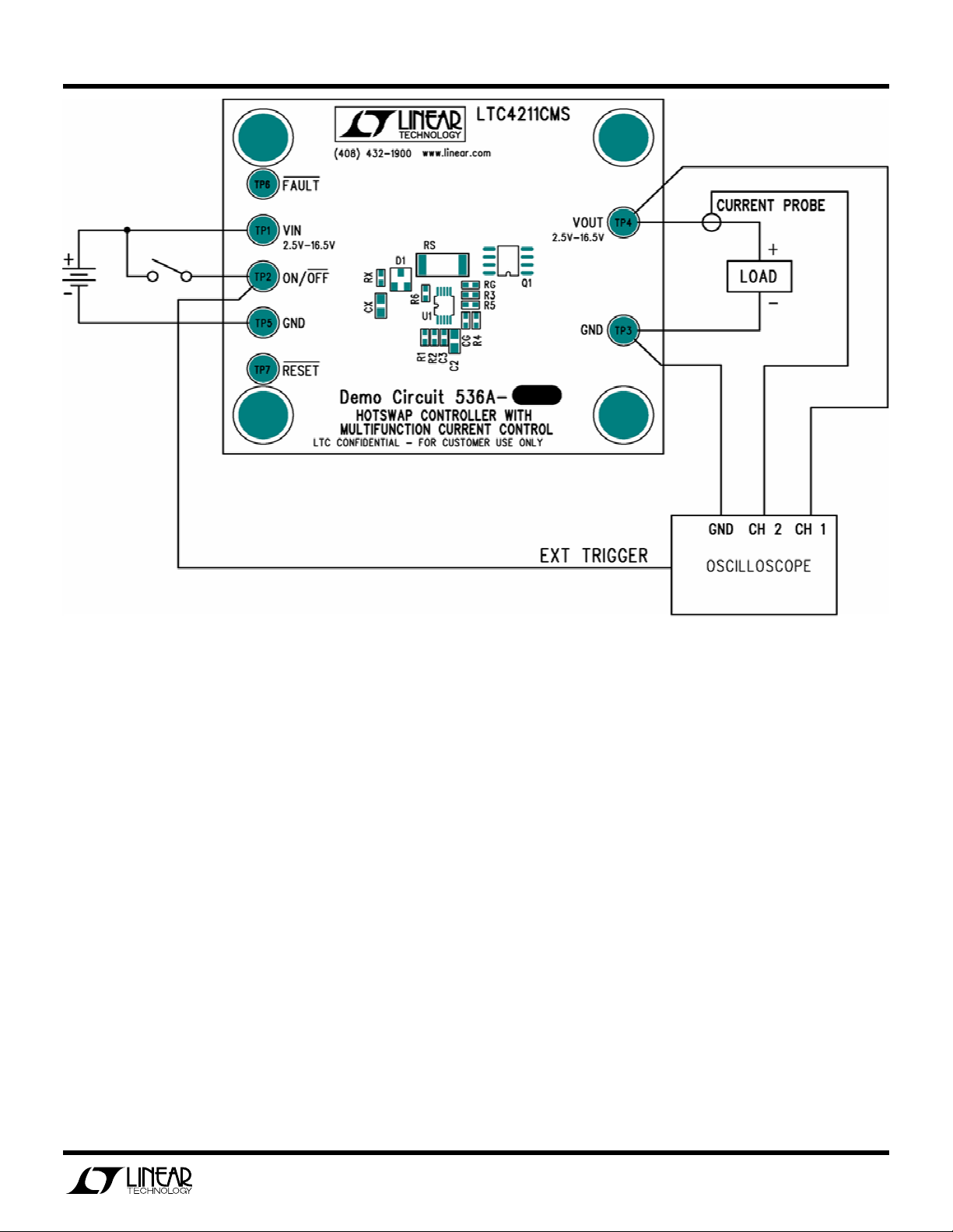
Demonstration circuit 536 is easy to set up to evaluate the performance of the LTC4211. Refer to Figure 1 for proper
measurement equipment setup and follow the procedure below:
1.
The DC536 is factory setup to operate in a 5 volt
system at current levels up to 5 amps. If the
LTC4211 is to be evaluated at a different operating
condition, follow 2-6 below, otherwise skip to 7.
2.
If evaluating at a voltage other than 5V, R3 must be
adjusted for proper RESET PIN response. Select
R3=V
•15K/1.223-15K, where V
MIN
is the mini-
MIN
mum output voltage expected for normal operation.
3.
The ON pin operates as a precision comparator and
can accurately provide an adjustable under voltage
lockout. The DC536 is initially configured to turn on
at 4.15V
. If 3.3V logic will drive this pin, R1 can
MIN
be replaced with a short. If the ON pin will be used
to provide under voltage lockout, then select R1
such that R1=V
•10K/1.39-10K, where V
UVLO
UVLO
the minimum turn on voltage. Refer to the data
sheet figure 3 for common configurations
4.
If the DC536 will operate at other than 7Amps max,
increase the value of R
SENSE
=0.99•I
/40mV for a
LOAD
1% tolerance current sense resistor.
5.
If the DC536 will be operating above 7Amps, replace Q1 with a suitable DD package MOSFET such
as the FDB8030L suitable for up to 20Amps. There
is a DD package footprint on the back of the board.
6.
The soft start and power good (RESET release) delay is factory set to 6.2ms. This delay can be adjusted by changing C
refer to the data sheet
TIMER
Table 1 for common values and the SYSTEM
TIMING section for more detailed information.
is
7.
After any necessary component changes have been
made, connect a suitable load between VOUT and
GND. This may be a passive resistive load or an active electronic load box.
8.
Connect a power supply capable of supplying
1.5•I
between the VIN and GND turrets. The
LOAD
minimum current capability of the supply must accommodate the tolerance of the circuit breaker
threshold of ±20%. With the 7mΩ factory installed
sense resistor, the overload circuit breaker will trip
at between 5.7A to 8.5Amp (7Amp nominal).
Connect the ON/OFF turret to the VIN turret to
enable power to the load. A function generator can
be used to generate a single event and trigger a
scope. The DC536 provides convenient turrets for
observing the FAULT, RESET and VOUT signals.
9.
The following experiments can be run. Turn on
into a nominal load. Turn on into an overload.
Turn on into a short circuit. Turn on into a nominal load and increase the load until the LTC4211
trips off. A digital storage scope provides a convenient means of observing the turn on and overload events. Observe the input or output current
using a current probe. A current transformer can
be used to observe turn on current transients if a
current probe is not available.
2
Page 3
QUICK START GUIDE FOR DEMONSTRATION CIRCUIT 536
HOT SWAP CONTROLLER WITH MULTIFUNCTION CURRENT CONTROL
Figure 1. Test Setup of the DC536.
3
Page 4
QUICK START GUIDE FOR DEMONSTRATION CIRCUIT 536
HOT SWAP CONTROLLER WITH MULTIFUNCTION CURRENT CONTROL
4
Page 5
QUICK START GUIDE FOR DEMONSTRATION CIRCUIT 536
HOT SWAP CONTROLLER WITH MULTIFUNCTION CURRENT CONTROL
5
Page 6

Mouser Electronics
Authorized Distributor
Click to View Pricing, Inventory, Delivery & Lifecycle Information:
Analog Devices Inc.:
DC536A-B
 Loading...