

Page 1
QUICK START GUID
E
A
r
FOR DC1589
LTC4425EDD: Linear Supercap
Charger With Current-Limited
Ideal Diode And V/I Monito
DESCRIPTION
Demonstration Circuit DC1589A is a Linear Supercap Charger with Current-Limited Ideal Diode and V/I Monitor,
featuring the LTC®4425.
PERFORMANCE SUMMARY
SYMBOL PARAMETER CONDITIONS MIN TYP MAX UNITS
Vin Input Voltage Range 2.7 5.5 V
Icharge Supercap Charge current 2 A
VOUT Supercap Stack Output Voltage 1.2 5.4 V
V(MID) Supercap Midpoint Voltage
Specifications are at TA = 25°C
0.6 2.7 V
QUICK START PROCEDURE
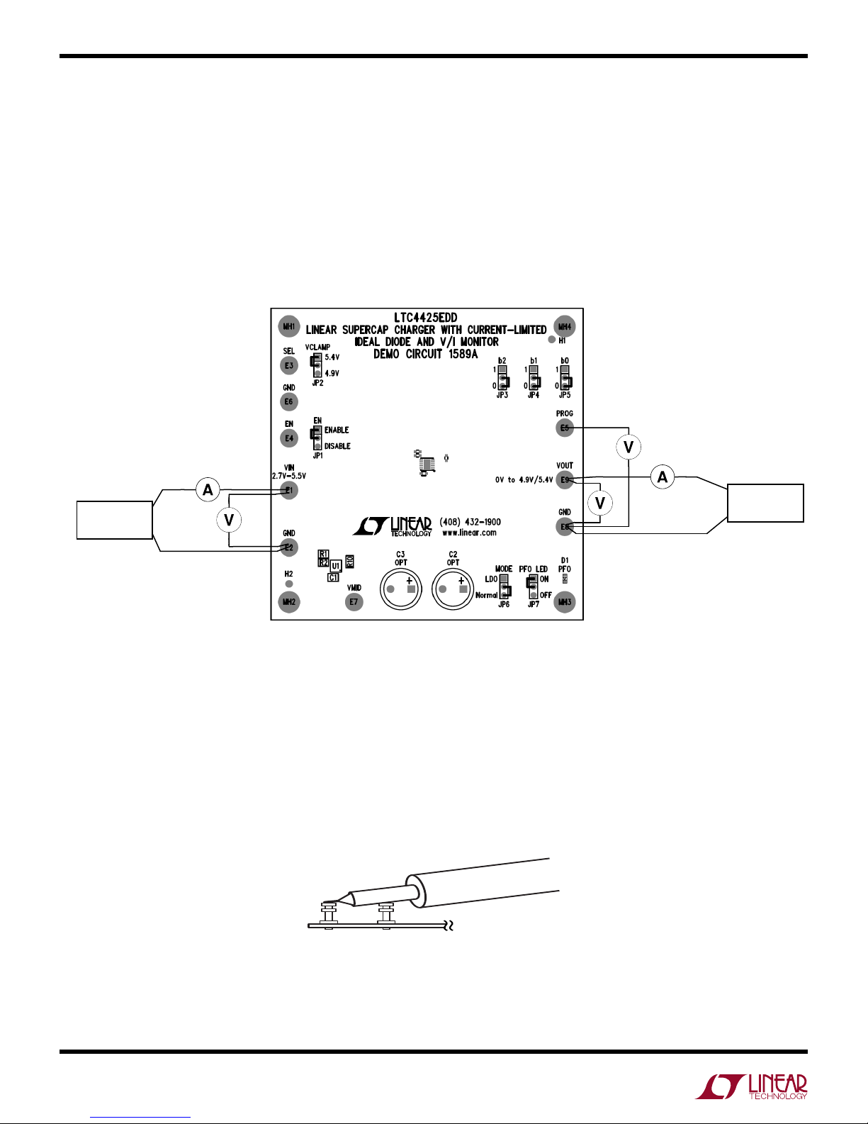
Refer to Figure 1 for the proper measurement
equipment setup and jumper settings and follow the
procedure below.
NOTE.
When measuring the input or output voltage ripple, care
must be taken to avoid a long ground lead on the oscilloscope
probe. Measure the input or output voltage ripple by touching the
probe tip directly across the VBUS or VOUT(x) and GND terminals.
See Figure 2 for proper scope probe technique.
1. Set b[2-0] jmpers (JP3, JP4, JP5) to “1”. Set
MODE (JP6) to “LDO”. Set LD1 to 0A, and PS1
to 5V. Observe VOUT (VM3) = 3.3V, I(VIN)
(AM1) = 2A, and V(PROG) (VM2) = 1V. Note:
The supercapacitor COUT1 will charge in approximately 0.5 seconds, so please observe
these signals within a few seconds of setting
PS1 to 5V.
2. Set PS1 to 0V. Observe D1 (PFO) should be lit
due to input ‘power failure’
3. Set LD1 to 1A. Observe VOUT. VOUT should
decrease to 0V, in about 1 second.
1
Page 2
A
AM1
-
+
+
PS1 +
4.35V - 5.5V supply
1A -
VM1
-
LTC4425EDD
-
VM2
+
+
-
+
VM3
-
AM2
+ LD1
0V - 5V
- 2
Note: All connections from equipment should be Kelvin connected directly to the board
pins which they are connected on this diagram and any input or output leads should be
twisted pair.
Figure 1. Proper Measurement Equipment Setup for DC1550A
Figure 2. Measuring Input or Output Ripple
2
VIN
GND
Page 3
LTC4425EDD
VOUT
E9
E8
0V to 4.9V / 5.4V
C4
COUT 1
OPT
0.55F
HS206F
0603
10uF
5.5V
5%
R14
511
1
2
D2
D1
BAT 54C
12
PFO
V+
ON
C2
OPT
5%
R13
PFO LED
JP7
OFF
C1
2.2u F
1k
11 12
U1
LT C4425EDD
6.3V
20%
+
8
1
2
PFO
VOUT
VOUT
VINVIN
PFI
9
C3
+
10
VMID
PFI_RET
7
VMID
E7
OPT
R12
2.1MEG
Fax: (408)434-0507
Milpitas, CA 95035
Phone: (408)432-1900
1630 McCarthy Bl vd.
LDO
Normal
JP6
MODE
VIN
OPT
R11
1.2MEG
5
FB
All Capacitors are 0402, 10%
13
GND
Unl ess Noted: Al l Resistors ar e 0402, 1%, 1/16W
EN
SEL
4
PROG
6
3
R10
10k
2k
R9
LTC Confidential-For Customer Use Only
TECHNOLOGY
LTC4425EDD: LINEAR SUPERCAP CHARGER WITH
CURRENT-LIMITED IDEAL DIODE AND V/I MONITOR
SCHEMATIC
TITLE:
G. Barbehenn
APPRO VALS
CONTRACT NO.
DRAWN:
CHECKED:
APPROVED :
ENGIN EER:
DC1589A
DWG NO. REV
A
SIZE
G. Barbehenn
DESIGN ER:
11
SHEET OF
Monday, November 23, 2009
DAT E:
GND
A
R2
R1
1.5MEG
VIN
2.7V - 5.5V
E2
GND
E1
VIN
1.2MEG
VIN
R5
R3
10k 5%
E3
E4
SEL
VIN
10k 5%
E5
EN
PROG
VCLAMP
EN
b0
1
R8
2.49k
b1
R7
1k
b2
11
JP2
5.4V
4.9V
JP1
ENABLE
DIS ABLE
JP5
0
JP4JP3
0
0
R6
5%
1MEG
R4
5%
1MEG
E6
GND
CUSTOMER NOTICE
THIS CIRCUIT IS PROPRIETARY TO LINEAR TECHNOLOGY AND
LINEAR TECHNOLOGY HAS MADE A BEST EFFORT TO DESIGN A
CIRCUIT THAT MEETS CUSTOMER-SUPPLIED SPECIFICATIONS;
HOW EVER, IT R EMAINS T HE CUST OMER' S RESPONSIBIL ITY TO
VERIFY PROPER AND RELIABLE OPERATION IN THE ACTUAL
APPLICATION. COMPONENT SUBSTITUTION AND PRINTED
CIRUIT BOARD LAYOUT MAY SIGNIFICANTLY AFFECT CIRCUIT
*
100mA
600mA
500mA
1
0
0
1000mA
1100mA
0
1
1
01
0
0
0
1
Charge current
0
b0
0
b1
0
Char ge cu rr ent = 1000 / R pr og
b2
SUPPLI ED FOR USE W ITH L INEAR TECHNO LOGY PART S.
PERFORMANCE OR RELIABILITY. CONTACT LINEAR
TECHNOLOGY APPLICATIONS ENGINEERING FOR ASSISTANCE.
2000mA
1600mA
1500mA
0
1
1
1
0
1
1
1
1
Defau lt
*
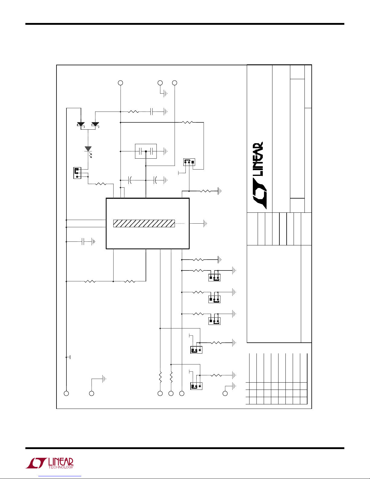
Figure 3. Circuit Schematic
3
Page 4
LTC4425EDD
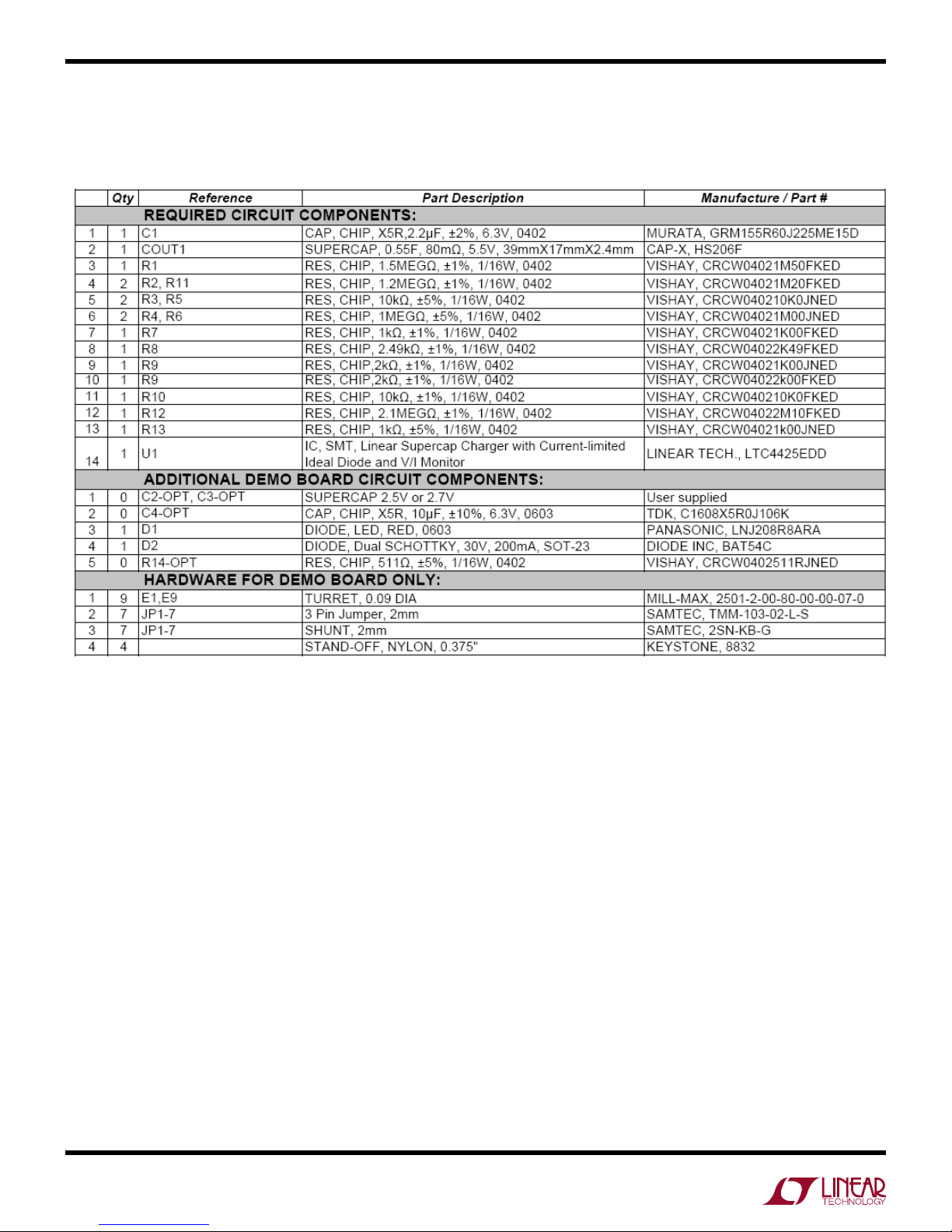
Figure 4. Bill of Materials
4
Page 5

Mouser Electronics
Authorized Distributor
Click to View Pricing, Inventory, Delivery & Lifecycle Information:
Analog Devices Inc.:
DC1589A
 Loading...