

Page 1
QUICK START GUIDE FOR DEMONSTRATION CIRCUIT 1409
DESCRIPTION
LTC3788
Demonstration circuit DC1409 is DC/DC boost
converter featuring the LTC3788 constant frequency current mode boost controller. The
DC1409A operates over 5V to 24V input and provides 8A to 10A of output current at 12V output.
Also, the DC1409A provides a second 24V output
capable of delivering 3A to 5A. The 300kHz con-
outputs can be connected together to generate
single output with two phase operation. Please
consult LTC factory for details.
The DC1409 has small circuit footprint. It is a high
performance and cost effective solution for Telecom, Automotive and Power Over Ethernet applications.
stant frequency operation results in small and efficient circuit. The converter provides high output
voltage accuracy (typically ±3%) over wide load
range with no minimum load requirement.
The demonstration circuit can be easily modified
Design files for this circuit board are available.
Call the LTC factory.
PowerPath is a trademark of Linear Technology Corporation
to generate different output voltages. Also, the two
Table 1. Performance Summary
PARAMETER CONDITION VALUE
Minimum Input Voltage DC1409A-A I
Maximum Input Voltage I
V
OUT1
V
Typical Output Ripple V
V
Nominal Switching Frequency 350kHz
OUT2
OUT1
OUT2
= 0A to 3A,
OUT1
I
= 0A to 8A
OUT2
= 0A to 5A
OUT1
I
= 0A to 10A
OUT2
VIN = 5V to 24V, I
VIN = 5V to 12V, I
VIN = 6V, I
VIN = 12V, I
OUT
OUT
= 3A
OUT1
OUT2
= 8A
= 3A
= 8A
5V
24V
24V ±3%
12V ±3% (see text)
200mV
200mV
P–P
P–P
QUICK START PROCEDURE
Demonstration circuit DC1409 is easy to set up to
evaluate the performance of the LTC3788. For
proper measurement equipment setup refer to
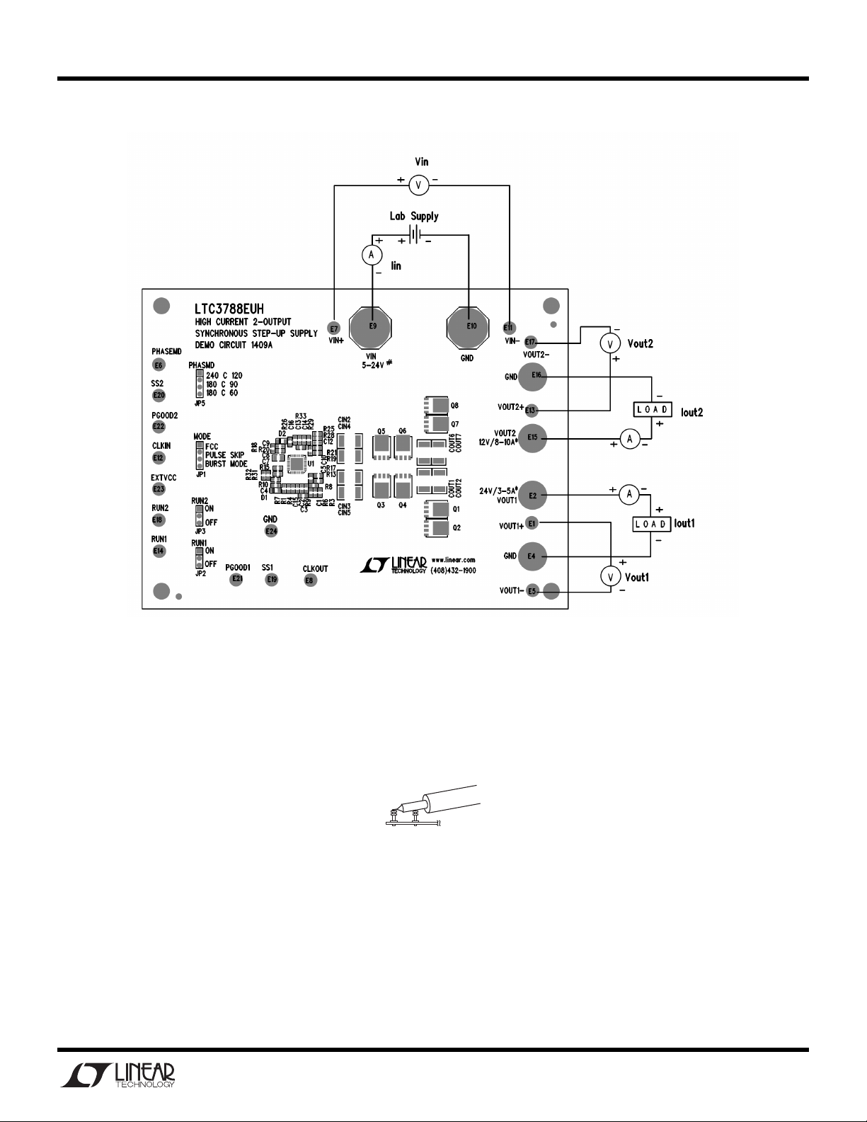
Figure 1 and follow the procedure below:
NOTE:
ripple, care must be taken to minimize the length
of oscilloscope probe ground lead. Measure the
input or output voltage ripple by connecting the
When measuring the input or output voltage
1
Page 2

QUICK START GUIDE FOR DEMONSTRATION CIRCUIT 1409
probe tip directly across the VIN or VOUT and
GND terminals as shown in Figure 2.
1.
With power off, connect the input power supply
to Vin and GND.
2.
Check the Vcc Bias voltage-setting jumper JP5.
Move it into Vin position if required.
3.
Turn the input power source on and slowly increase the input voltage. Be careful not to exceed 24V.
NOTE:
does not exceed 24V. If higher operating voltage is required, power components with higher
voltage ratings should be used.
4.
Set the input voltage to 6V and check for the
proper output voltage of 12V and 24V.
Make sure that the input voltage Vin
If there is no output, temporarily disconnect the
load to make sure that the load is not set too
high.
5.
Once the proper output voltage is established,
adjust the load and observe the output voltage
regulation, ripple voltage, efficiency and other
parameters.
2
Page 3
QUICK START GUIDE FOR DEMONSTRATION CIRCUIT 1409
VIN
GND
Figure 1. Proper Measurement Equipment Setup
Figure 2. Measuring Input or Output Ripple
3
Page 4
QUICK START GUIDE FOR DEMONSTRATION CIRCUIT 1409
Efficiency
CHANGING THE OUTPUT VOLTAGE
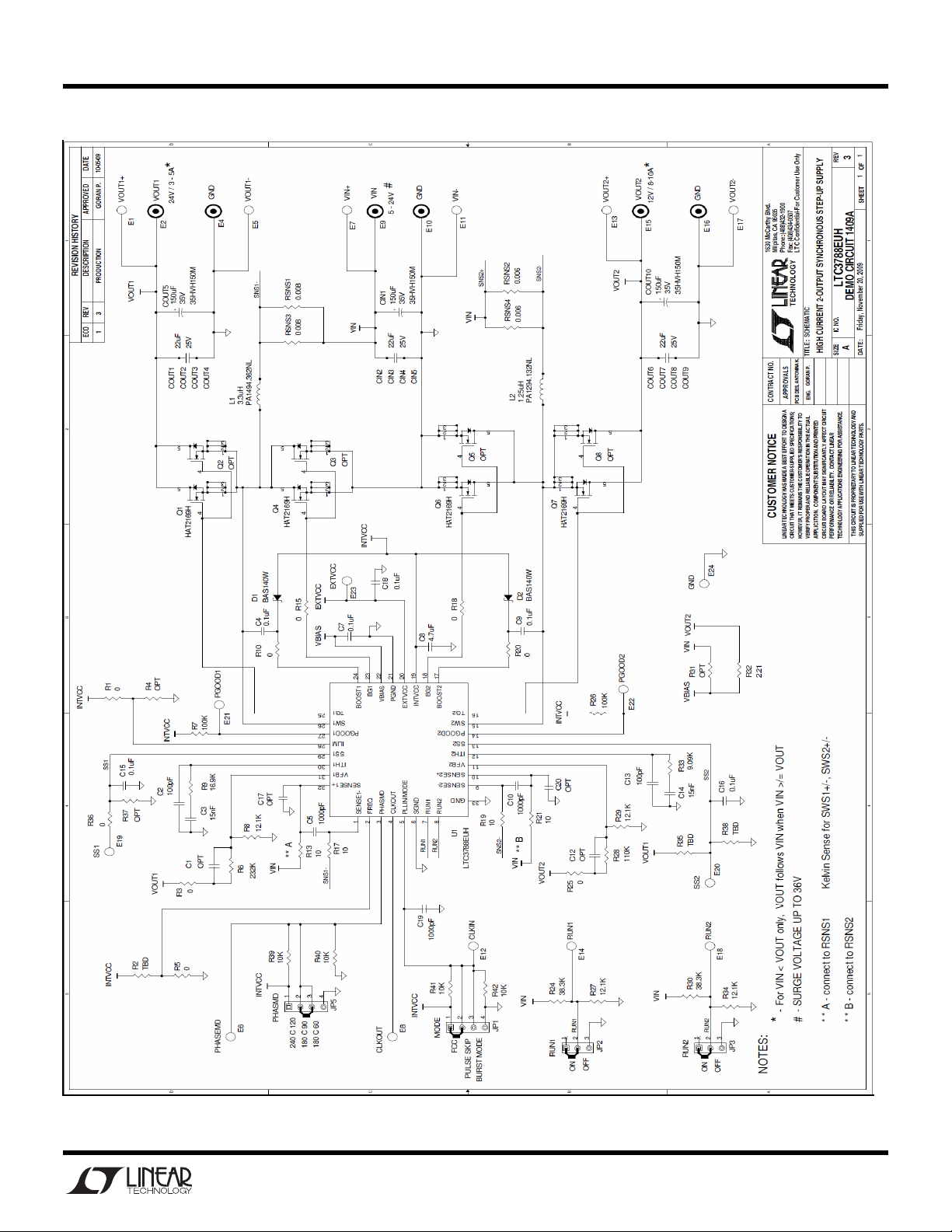
To set the output voltage lower than 12V or 24V, change the bottom voltage divider resistors connected to LTC3788 FB pin (see the schematic on page 6).
To get higher than 12V and 24V output voltages MOSFETs and capacitors with higher voltage ratings may be required. Please contact LTC factory for details.
Note that the output voltage will start following the input voltage when input voltage is greater than
the voltage set by the voltage divider. In this mode (wire mode) the output rectifier MOSFET is
turned continuously ON. The only losses in this mode are due to the current sense resistors, inductor and output MOSFET DC resistance.
CONVERTER EFFICIENCY AND OUTPUT CURRENT
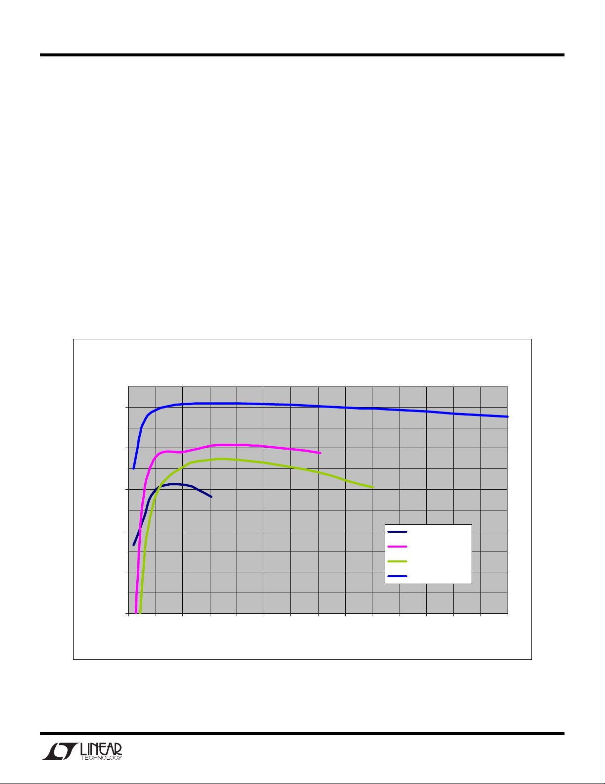
The DC1409 output current capability depends on the input voltage and proper cooling. Typical performance of DC1409A is shown in Figure 3. As can be seen from Figure 3, the output current capability depends on the input voltage. Also, when input voltage is equal or higher than the output
voltge setting (wire mode) the efficiency is very high (99%) since the converter is not really running
and the output MOSFET is shorting Vin to Vout (blue trace in Figure 3).
LTC3788 Efficiency 12V and 24V output
99%
97%
95%
93%
91%
89%
0 1 2 3 4 5 6 7 8 9 10 11 12 13 14
Iout [A]
5V in, 24V out
12V in, 24V out
5V in, 12V out
12V in, 12V out
Figure 3. DC1409A Efficiency
4
Page 5
QUICK START GUIDE FOR DEMONSTRATION CIRCUIT 1409
OUTPUT LOAD STEP RESPONSE
The load step response of DC1409A is very good even though relatively small amount of output
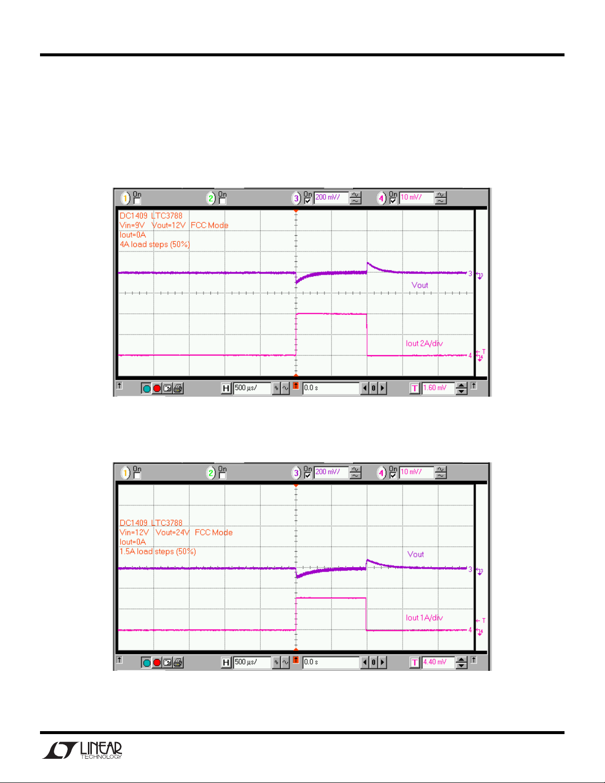
capacitance is present at the output. If higher load steps need to be handled more output capacitance can be added in order to keep the voltage transients at the desired level. The load step transients are shown in Figure 5 and Figure 6. Also, note that load step response even from 0% load is
excellent thanks to synchronous rectification.
Figure 5. 12V Output load step response
Figure 6. 24V Output load step response
5
Page 6
QUICK START GUIDE FOR DEMONSTRATION CIRCUIT 1409
6
Page 7

Mouser Electronics
Authorized Distributor
Click to View Pricing, Inventory, Delivery & Lifecycle Information:
Analog Devices Inc.:
DC1409A
 Loading...