

Page 1
QUICK START GUIDE FOR DEMONSTRATION CIRCUIT 1090A
JP1
JP2
JP3
PUSH BUTTON ON/OFF CONTROLLER WITH MICROPROCESSOR INTERRUPT
DESCRIPTION
LTC2954-2
Demonstration Circuit 1090A features the LTC2954-2,
a push button ON/OFF controller that manages system
power via a push button interface. An enable output
toggles system power while an interrupt output provides a debounced push button status. The interrupt
output can be used in menu driven applications to request a system power down. A power kill input allows
a microprocessor or system to reset the enable output, effectively powering down the system. Independently adjustable On and Off timers allow dependable
push button control of the enable output and resistance to accidental toggling of system power.
QUICK START PROCEDURE
Demonstration circuit 1090A is easy to set up to evaluate the performance of the LTC2954-2:
1.
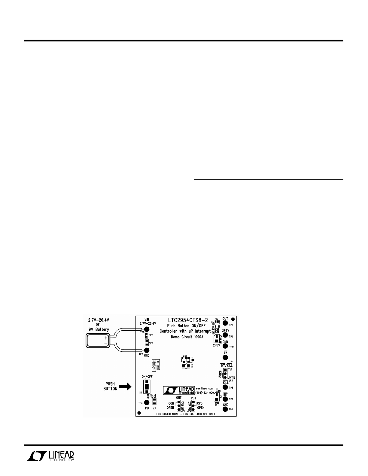
Place jumpers in the following positions:
CON
CPD
UNTIE
The LTC2954 operates over a wide 2.7V to 26.4V
input voltage range to accommodate a wide variety
of input power supplies. Very low quiescent current
(6µA typical) makes the LTC2954 ideally suited for
battery powered applications. Two versions of the
part are available to accommodate either positive or
negative enable polarities. The inversion of /EN of
the LTC2954-2 is found in the LTC2954-1
Design files for this circuit board are available.
Call the LTC factory
LTC is a trademark of Linear Technology Corporation
2.
Connect the input power supply of 2.7V to 26.4V
across VIN and GND or a 9V battery to the battery
connector.
3.
Push and hold the push button once to turn on the
green LED.
4.
Push and hold again on the push button to turn off
the green LED.
.
Figure 1. DC1090A Example Setup
1
Page 2

QUICK START GUIDE FOR DEMONSTRATION CIRCUIT 1090A
PUSH BUTTON ON/OFF CONTROLLER WITH MICROPROCESSOR INTERRUPT
OPERATING PRINCIPLES
On the DC1090A, a push button switch shorts the /PB
pin to ground which in turn sets the /EN pin low.
Shorting /PB to ground a second time and holding
subsequently resets the /EN pin high. The /EN pin is
used to drive the gate of a P-channel MOSFET to control the power path to a DC/DC converter. The turn on
and off of the circuit is displayed with a green LED
(D2).
The duration that /PB must be shorted to ground in
order to turn on/off the DC/DC converter is independently programmed by two external capacitors C1 and
C2 and selected on the DC1090A with jumper JP1 and
JP2.
An internal 500ms timer blanks (ignores) the /KILL
signal during system power up. This allows sufficient
time for the DC/DC converter and a µP to perform
power up tasks. During turn off, a power down timer
provides a delay from interrupting the µP (/INT=low)
to turning off the DC/DC converter (/EN=high). This
delay gives the µP time to perform power down and
housekeeping tasks. On the DC1090A, JP1 selects the
turn on timer, while JP2 is used to adjust the power
down /PB duration. The red LED D1 shows the state
of the /INT pin. A µP can turn off the converter with
no delay by asserting /KILL low.
By tying /KILL to /INT through JP3, /KILL is forced low
during the /INT blanking time and thus forces a turn
off.
The RC (R
and C
RPP
) at VIN on the DC1090A provides
RPP
a reverse polarity protection to the LTC2954-2. If
power is connected in an application such that the polarities are ensured to be in the correct configuration,
this RC may be removed from the circuit.
An additional RC (RF and CF), located at the /PB pin,
acts as a filter and used in an application where the
switch is located far from the LTC2954-2. In such a
case, the RC would be placed next to the switch rather
than the part. If the switch is located near the
LTC2954-2, then the RC may be removed from the
circuit.
An LDO (U2) is used on the DC1090 to provide a pullup voltage of 2.6V which is well below the absolute
maximum on the /INT, /EN, and /KILL pins for the full
range of input voltage of 2.7V to 26.4V. In an application, pull these pins up to a voltage no higher than
their rated absolute maximum shown in the data
sheet. (If the interface pins on the DC1090A are pulled
up to an external supply higher than 5V, LEDs D1 and
D2 should be removed.)
Table 1. DC1090A Typical Performance Summary (TA = 25°C)
PARAMETER CONDITION VALUE
Input Voltage VIN 2.7V to 26.4V
V
, /PB Turn On
Output Voltage
/PB Turn On Time
/PB Turn Power Down Time
*The additional Cap. Adjust time is selected by an external capacitor. The DC1090A adjust times have been pre-selected with 0.033uF at ONT and 0.47uF at CPD to provide
additional 212ms and 3014ms turn on and turn power down time respectively. The additional time is calculated with the following equations as shown in the LTC2954 data
sheet:
C
= 1.56 x 10⁻⁴ [µF/ms] • (t
ONT
C
= 1.56 x 10⁻⁴ [µF/ms] • (t
PDT
– 1ms)
ONT
– 1ms)
PDT
OUT
V
, /PB Turn On
2P6V
JP1 on OPEN
JP1 on CAP*
JP2 on OPEN
JP2 on CAP*
VIN - VDS
2.6V ± 2%
32ms
32 + 212ms
32ms
32 + 3014ms
2
Page 3
QUICK START GUIDE FOR DEMONSTRATION CIRCUIT 1090A
PUSH BUTTON ON/OFF CONTROLLER WITH MICROPROCESSOR INTERRUPT
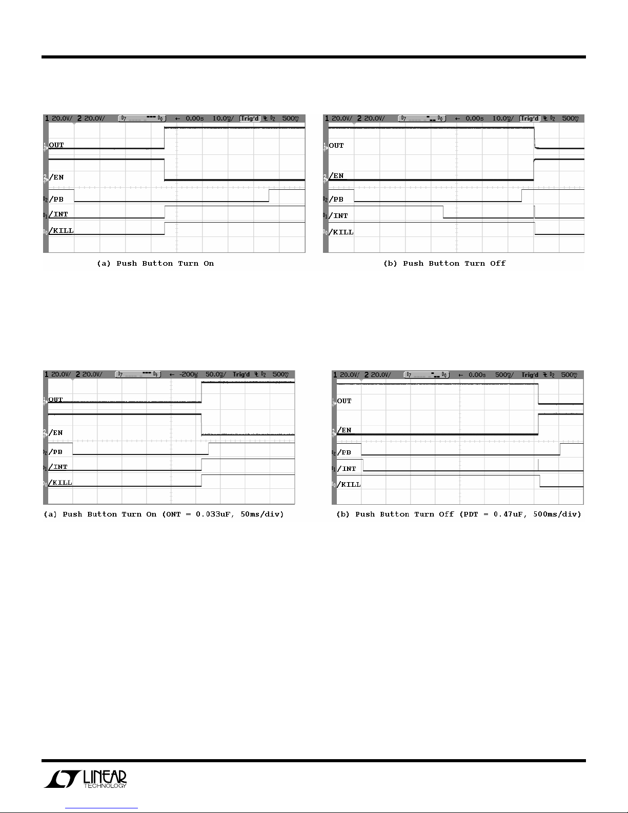
Figure 2. Push Button Turn On/Off with ONT and PDT Open (time scale at 10ms/div)
Figure 3. Push Button Turn On/Off with Capacitors on ONT and PDT
3
Page 4
QUICK START GUIDE FOR DEMONSTRATION CIRCUIT 1090A
PUSH BUTTON ON/OFF CONTROLLER WITH MICROPROCESSOR INTERRUPT
4
Page 5

Mouser Electronics
Authorized Distributor
Click to View Pricing, Inventory, Delivery & Lifecycle Information:
Analog Devices Inc.:
DC1090A
 Loading...