

Page 1
DB-960-70W
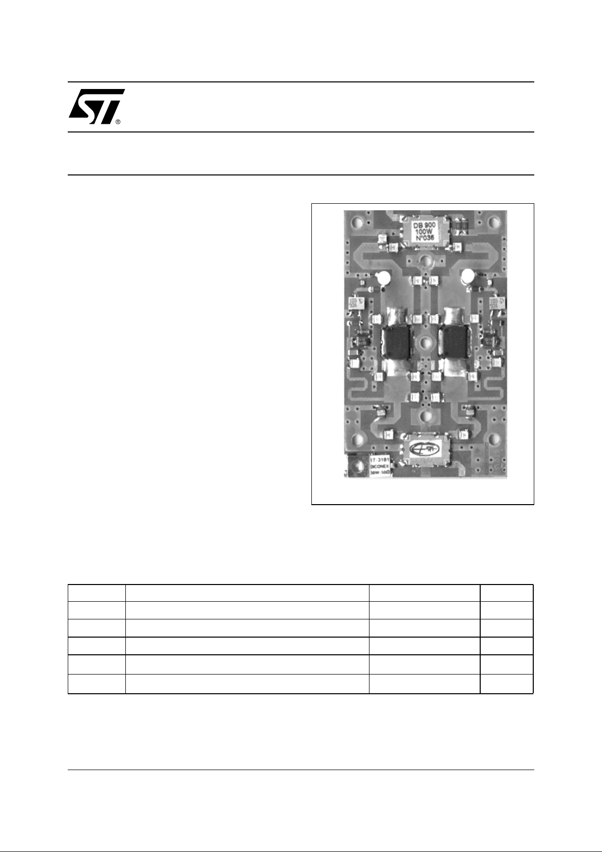
70W / 26V / 925-960 MHz PA using 2x PD57045S
N-CHANNEL ENHANCEMENT-MODE LATERAL
MOSFETs
• EXCELLENT THERMAL STABILITY
• COMMON SOURCE CONFIGURATION
• P
= 70 W min. with 13 dB gain over 925-960
OUT
MHz
• 10:1 LOAD VSWR CAPABILITY
• BeO FREE AMPLIFI E R.
DESCRIPTION
The DB-960-70W is a common source N-Channel
enhancement-mode lateral Field-Effect RF power
amplifier designed for GSM & E-GSM base station
applications.
The DB-960-70W is desig ned in coope ration with
Européenne de Télécommunications S.A
(www.etsa.fr), for high gain and broadband
performance operating in common source mode
at 26 V, capable of withstanding load mismatch up
to 10:1 all phases and with harmo nics lower t han
30 dBc.
The
MECHANICAL SPECIFICATION
L=80 mm W=50 mm H=10 mm
LdmosST
ORDER CODE
DB-960-70W
FAMILY
PRELIMINARY DATA
ABSOLUTE MAXIMUM RATINGS (T
Symbol Parameter Value Unit
V
DD
I
D
P
DISS
T
CASE
P
amb
November, 20 2002
Supply voltage 32 V
Drain Current 9 A
Power Dissipation 135 W
Operating Case Temperature -20 to +85
Max. Ambient Temperature +55
CASE
= 25oC)
o
C
o
C
1/5
Page 2
DB-960-70W
0
)
ELECTRICAL SPECIFICATION (T
= +25oC, Vdd = 26V, Idq = 2 x 200mA)
amb
Symbol Test Conditions Min. Typ. Max. Unit
FREQ. Frequency Range 925 960 MHz
P
Gain
P
1dB
Flatness
Flatness
ND at P
IRTL
Harmonic
VSWR
Spurious
IMD
1dB
3
OUT
= 75 W
12.5 13 dB
Over frequency range: 925 - 960 MHz 70 75 W
Over frequency range and @ P
P
from 0.1W to 75W
OUT
P
1dB
Input return Loss P
P
= 75 W
OUT
from 0.1W to 75W
OUT
Load Mismatch all phases @ P
10:1 VSWR all phases and P
P
= 75 WPEP
OUT
= 75 W
OUT
= 75 W
OUT
from 0.1 to 75W
OUT
+/- 0.5 dB
1dB
45 50 %
-20 -15 dB
-40 -30 dBc
10:1
-76 dBc
-25 dB c
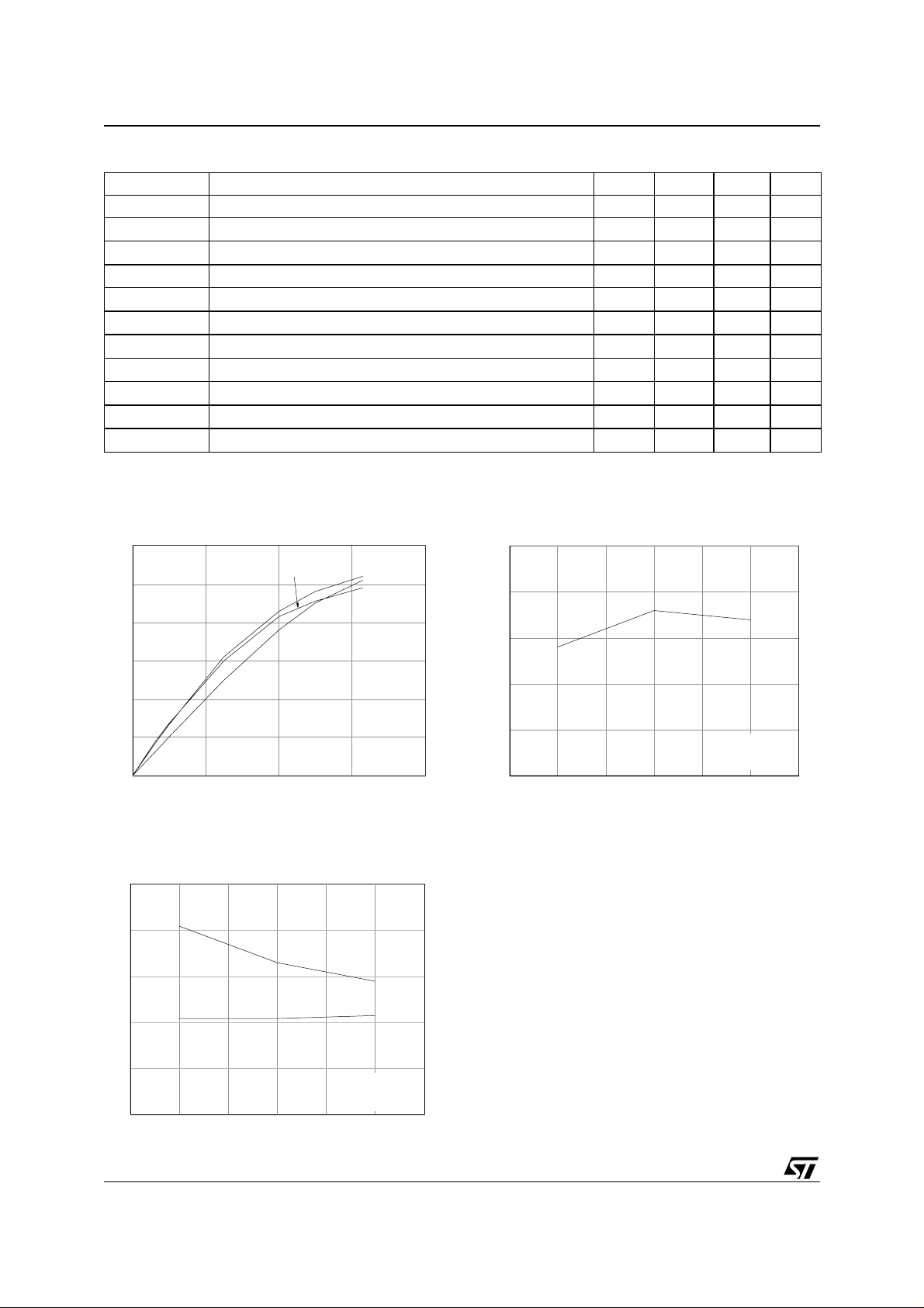
TYPICAL PERFORMANCE
Output Power versus Input Power Power Gain versus Frequency (Pout = 75W)
Pout (W)
120
100
80
60
40
960 MHz
940 MHz
920 MHz
Gp (dB)
15
14
13
12
20
0
02468
Pin (W)
Vdd = 26 V
Idq = 2 x 200 mA
P1dB and Efficiency versus Frequency
P1dB (W)
120
100
P1dB
80
Eff.
60
40
Vdd = 26 V
Idq = 2 x 200 mA
20
910 920 930 940 950 960 970
F (MHz)
2/5
Nd (%
11
Vdd = 26 V
Idq = 2 x 200 m A
10
910 920 930 940 950 960 97
F (MHz)
80
70
60
50
40
30
Page 3

TEST FIXTU R E CO M PONENT LAY O UT
CV1
CV2
DB-960-70W
TEST CIRCUIT PHOTOMASTER
Ref. ETSA c07/2000 - Ed1
Ref. ETSA c07/2000 - Ed1
3/5
Page 4

DB-960-70W
TEST CIRCUIT COMPONENT PART LIST
COMPONENT DESCRIPTION
T1, T2 PD57045S TRANSISTOR
C1, C2, C23, C24 47pF - 500V CERAMIC CHIP CAPACITOR
C3, C4 2.2pF - 500V CERAMIC CHIP CAPACITOR
C5, C6, C17, C18 100pF - 500V CERAMIC CHIP CAPACITOR
C7, C8, C9, C10, C11, C12, C13, C14 10pF - 500V CERAMIC CHIP CAPACITOR
C15, C16 100nF - 63V CERAMIC CHIP CAPACITOR
C19, C20 1µF / 35V ELECTROLYTIC CAPACITOR
C21, C22 4.7pF - 500V CERAMIC CHIP CAPACITOR
C26, C27 3.3pF - 500V CERAMIC CHIP CAPACITOR
C25 0.5pF - 500V CERAMIC CHIP CAPACITOR
CV1, CV2 ADJUSTABLE CAPACITOR 0.6 - 4.5pF / 500V
P1, P2 10K Ohms MULTITURN POTENTIOMETER
R1,R7 100 Ohms 1/4W 1206 SMD CHIP RESISTOR
R2 50 Ohms 30W - 4GHz LOAD
R3, R4 4.7K Ohms 1/4W 1206 SMD CHIP RESISTOR
R5, R6 10K Ohms 1/4W 1206 SMD CHIP RESISTOR
D1, D2 ZENER DIODE 5V - 500 mW SOD80
SM1, SM2 90° SMD HYBRID COUPLER ANAREN Xinger 1304-3
BOARD METCLAD MX3-30-C1/10C THK 0.762 mm Cu 35µ
SUBSTRATE TEFLON-GLASS Er = 2.55
BACK SIDE COPPER FLANGE 2 mm THICKNESS
CERAMIC CHIP CAPACITORS ATC100B or EQUIVALENT
4/5
Page 5

DB-960-70W
Information furnished is believed to be ac curate and reli able. Howev er, STMicroel ectronics assumes no responsibilit y for the cons equences
of use of such information nor for any infringement of patents or other rights of third parties which may result from its use. No license is granted
by implic ation or otherwise under any patent or patent rights of STMi croelectr onics. Specifications mentioned in thi s publicati on are s ubject
to change without notice. This publication supersedes and replaces all information previously supplied. STMicroelectronics products are not
authorized for use as cri tical comp onents in life support dev i ces or systems wi t hout express written ap proval of STMi croelect ronics.
The ST log o i s registered trademark of STMicroelectronics
2001 STMicroelectronics - All Right s Reserved
All other names are the property of their respective owners.
Australi a - B razil - China - Finland - F rance - Germ any - Hong Kon g - India - Italy - Japan - Mala ysia - Malta - Morocco -
Singapor e - Spain - Sweden - Switzerl and - United Kingdom - U .S .A.
STMicroelectron ics GROUP OF COMPANIES
http://www.st.com
5/5
 Loading...