

Page 1

查询DB-2933-54供应商
General feature
■ Excellent thermal stability
■ Frequency: 1.6 - 54MHz
■ Supply voltage: 48V
■ Output power: 400W typ.
■ Input power 10W max.
■ Efficiency: 57% - 76%
■ IMD at 300WPEP < -26dBc
■ Load mismatch: 3:1all phases
DB-2933-54
RF POWER amplifier using 2 x SD2933
N-Channel enhancement-mode lateral MOSFETs
Description
The DB-2933-54 is a RF broadband power
amplifier intended for linear or nonlinear operation
over the band 1.6 to 54 MHz using 2x SD2933
gold metallized N-channel MOS field-effect
transistors. The temperature compensating
biasing circuit supports class B and class AB
operation.
DB-2933-54 is designed in cooperation with
Specific RF Devices.
(e-mail : [email protected])
Order Code
■ DB-2933-54
October 2006 Rev 1 1/13
www.st.com
13
Page 2

Contents DB-2933-54
Contents
1 Electrical data . . . . . . . . . . . . . . . . . . . . . . . . . . . . . . . . . . . . . . . . . . . . . . 3
1.1 Maximum ratings . . . . . . . . . . . . . . . . . . . . . . . . . . . . . . . . . . . . . . . . . . . . 3
2 Electrical characteristics . . . . . . . . . . . . . . . . . . . . . . . . . . . . . . . . . . . . . 4
3 Typical performance . . . . . . . . . . . . . . . . . . . . . . . . . . . . . . . . . . . . . . . . . 5
4 Photos of DB-2933-54 amplifier . . . . . . . . . . . . . . . . . . . . . . . . . . . . . . . . 7
5 DB-2933-54 class of operation . . . . . . . . . . . . . . . . . . . . . . . . . . . . . . . . . 8
6 SD2933 mounting recommendations . . . . . . . . . . . . . . . . . . . . . . . . . . . 9
6.1 Mounting recommendations . . . . . . . . . . . . . . . . . . . . . . . . . . . . . . . . . . . . 9
6.2 Mounting sequence . . . . . . . . . . . . . . . . . . . . . . . . . . . . . . . . . . . . . . . . . . 9
7 Package mechanical data . . . . . . . . . . . . . . . . . . . . . . . . . . . . . . . . . . . . 11
8 Revision history . . . . . . . . . . . . . . . . . . . . . . . . . . . . . . . . . . . . . . . . . . . 12
2/13
Page 3

DB-2933-54 Electrical data
1 Electrical data
1.1 Maximum ratings
Table 1. Absolute maximum ratings
Symbol Parameter Value Unit
P
IN
P
OUT
(1)
V
DD
V
GG
I
DD
P
DISS
1. VGG from 9 to 15V and PIN < 16W
Input power 16 W
Output power 500 W
Drain supply voltage 50 V
Gate biasing voltage 15 V
Drain current 20 A
Power dissipation 400 W
3/13
Page 4

Electrical characteristics DB-2933-54
2 Electrical characteristics
TA = +25 oC, VDD = 48V, I
= 2 x 900mA
DQ
Table 2. Electrical Specification
Symbol Test Conditions Min Typ Max Unit
Freq Frequency range 1.6 54 MHz
P
OUT
Gain P
ND P
H2 2
H3 3
VSWR Load mismatch all phases @ P
PIN = 10W 300 400 W
= 10W 16.2 ± 0.6dB dB
IN
= 10W 57 - 76 %
IN
ND
Harmonic @ P
RD
Harmonic @ P
= 300W -26 / -49 dBc
OUT
= 300W -13 / -58 dBc
OUT
= 300W 3:1
OUT
4/13
Page 5
DB-2933-54 Typical performance
y
(
)
O
(
)
Efficiency (% )
600
O
t
t
P
(W )
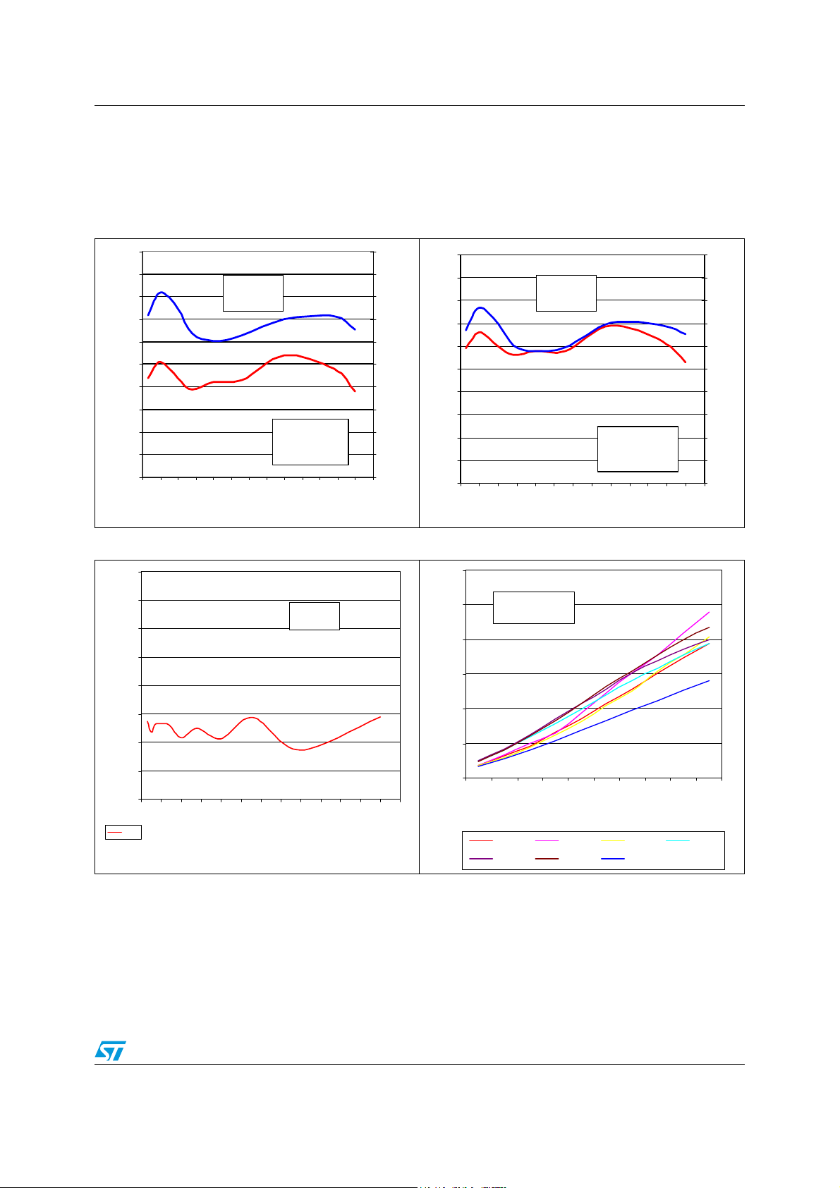
3 Typical performance
Figure 1. Output power & efficiency
60
59
58
57
56
55
54
53
Output Power (dBm )
52
51
50
vs frequency
- eff
- Pout
V dd =
40V
Idq = 2x
0 5 10 15 20 25 30 35 40 45 50 55 60 65
Frequenc y (M Hz)
mA
90
Pin = 10W
Figure 2. Output power & efficiency
vs frequency
100
90
80
70
60
50
40
30
20
10
0
60
59
58
57
%
dBm
56
55
54
Efficienc
utput Power
53
52
51
50
0 5 10 15 20 25 30 35 40 45 50 55 60 65
- eff
- Pout
Frequency (M Hz)
V dd =
Idq = 2x
Pin = 10W
48V
900
mA
100
90
80
70
60
50
40
30
20
10
0
Figure 3. IMD vs frequency Figure 4. Output power vs drain voltage
0
-5
-10
-15
-20
IM D (dBc)
-25
-30
-35
-40
0 5 10 15 20 25 30 35 40 45 50 55 60 65
IM D
Frequency (M H z)
Vdd =
48V
Idq = 2x
900
Pout = 300 WPEP
mA
500
400
ower
300
pu
200
u
100
0
10 14 18 22 26 30 34 38 42 46 50
Pin = 10W
Idq = 2x
1.6 M H z 5 M Hz 10 M Hz 20 M Hz
28 M Hz 40 M Hz 60 M Hz
mA
900
Drain vo ltage (V)
5/13
Page 6
Typical performance DB-2933-54
P
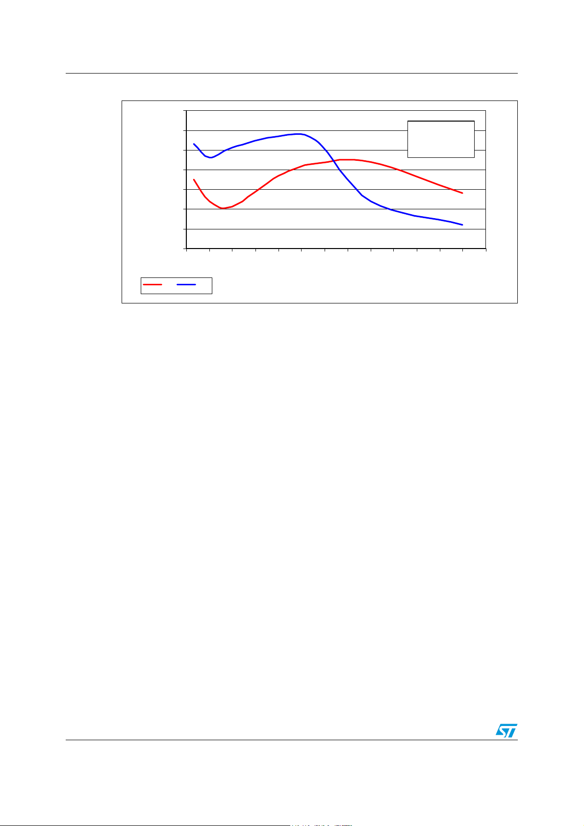
Figure 5. Harmonics vs frequency
0
Vdd =
-10
-20
Idq = 2x
Pout = 300 WPE
48V
900
mA
-30
-40
-50
Harmoni cs (dBc)
-60
-70
0 5 10 15 20 25 30 35 40 45 50 55 60 65
H2 H3
Frequency (MHz)
6/13
Page 7
DB-2933-54 Photos of DB-2933-54 amplifier
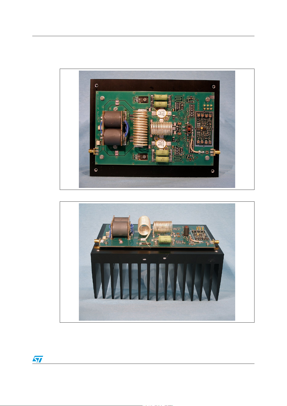
4 Photos of DB-2933-54 amplifier
Figure 6. Top view
Figure 7. Side view
7/13
Page 8

DB-2933-54 class of operation DB-2933-54
5 DB-2933-54 class of operation
● class B : a low bias point with ~100mA per transistor
● class AB : a higher bias point with ~ 900mA per transistor
To select a bias point, DB-2933-54 has a control port “BIAS”.
● The bias point is 2x 100 mA if “BIAS” is left open and in this case a DC voltage of ~5V
is present
● The bias point is 2 x 900 mA if “BIAS” is connected to ground.
"PA_ON" control port / ON-OFF bias current
● To switch-on biasing circuit, connect “PA_ON” to ground.
● To switch-off biasing circuit, left open “PA_ON”
8/13
Page 9

DB-2933-54 SD2933 mounting recommendations
6 SD2933 mounting recommendations
6.1 Mounting recommendations
● Ensure holes in heatsinks are free from burrs;
● Minimum depth of tapped holes in heatsinks is 6 mm;
● Use 4-40 UNC-2A cheese-head screws with a flat washer to spread the joint pressure;
● The minimum flatness of the mounting area is 0.02 mm;
● Mounting area roughness should be less than 0.5 µm (micro);
● Avoid, as much as possible, use of flux or flux solutions because flux can penetrate
even when hermetically sealed ceramic-capped transistors. Tin and wash the printedcircuit board BEFORE mounting the power transistors, then solder the transistor leads
without using flux;
● Transistor leads may be tinned by dipping them full-length into a solder bath at a
temperature of about 230°C. No flux should be used during tinning;
● Recommended heatsink compounds : WPSII (silicon free) from Austerlitz Electronics,
340 from Dow Corning etc.
6.2 Mounting sequence
● Apply a thin layer of evenly distributed heatsink compound to the flange;
● Position the device with flat washers in place;
● Tighten the screws until finger tight (0.05 Nm);
● Further tighten the screws until the specified torque is reached;
● For M174, M177 & M244 type of packages, torque should be minimum 0.6 Nm and
0.75 Nm max.
9/13
Page 10

SD2933 mounting recommendations DB-2933-54
Table 3. DMOS Packages - List of materials
Package
Typ e
M174
M174
(Moly
disk)
M177
M244
Description Flange Leadframe
0.500 DIA
4L NON
HERM
W/FLANGE
0.500 DIA
4L NON
HERM
W/FLANGE
(MOLY
DISK)
0.550 DIA
4L NON
HERM
W/FLANGE
2x
0.400x0.425
WIDE 2L
LAP N/H
FLANGE
Cu
Cu-Mo-
Cu
Cu-Mo-
Cu
(85%) -
Cu
(15%)
W
ALLOY 42
(Fe58 /
Ni42)
ALLOY 42
(Fe58 /
Ni42)
ALLOY 42
(Fe58 /
Ni42)
ALLOY 42
(Fe58 /
Ni42)
Ceramic
insulator
BeO
(99.5%
min)
BeO
(99.5%
min)
BeO
(99.5%
min)
BeO(99.5
% min)
Plating Torque (Nm)
Leads Flange Min Max
Au (100µ min) over
Ni (100µ min /
350µ max)
Au (100µ min) over
Ni (100µ min /
350µ max)
Au (60µ min) over
Ni (100µ min /
350µ max)
Au (60µ min) over
Ni (100µ min /
350µ max)
Ni(100µ min) + Pd
(10µ min)
Ni(100µ min) + Pd
(10µ min)
Au (100µ min)
over Ni (100µ min
/ 350µ max)
Au (60µ min) over
Ni (100µ min /
350µ max)
0.6 0.75
0.6 0.75
0.6 0.75
0.6 0.75
10/13
Page 11

DB-2933-54 Package mechanical data
7 Package mechanical data
In order to meet environmental requirements, ST offers these devices in ECOPACK®
packages. These packages have a Lead-free second level interconnect . The category of
second level interconnect is marked on the package and on the inner box label, in
compliance with JEDEC Standard JESD97. The maximum ratings related to soldering
conditions are also marked on the inner box label. ECOPACK is an ST trademark.
ECOPACK specifications are available at: www.st.com
11/13
Page 12

Revision history DB-2933-54
8 Revision history
Table 4. Revision history
Date Revision Changes
19-Oct-2006 1 Initial release
12/13
Page 13

DB-2933-54
Please Read Carefully:
Information in this document is provided solely in connection with ST products. STMicroelectronics NV and its subsidiaries (“ST”) reserve the
right to make changes, corrections, modifications or improvements, to this document, and the products and services described herein at any
time, without notice.
All ST products are sold pursuant to ST’s terms and conditions of sale.
Purchasers are solely responsible for the choice, selection and use of the ST products and services described herein, and ST assumes no
liability whatsoever relating to the choice, selection or use of the ST products and services described herein.
No license, express or implied, by estoppel or otherwise, to any intellectual property rights is granted under this document. If any part of this
document refers to any third party products or services it shall not be deemed a license grant by ST for the use of such third party products
or services, or any intellectual property contained therein or considered as a warranty covering the use in any manner whatsoever of such
third party products or services or any intellectual property contained therein.
UNLESS OTHERWISE SET FORTH IN ST’S TERMS AND CONDITIONS OF SALE ST DISCLAIMS ANY EXPRESS OR IMPLIED
WARRANTY WITH RESPECT TO THE USE AND/OR SALE OF ST PRODUCTS INCLUDING WITHOUT LIMITATION IMPLIED
WARRANTIES OF MERCHANTABILITY, FITNESS FOR A PARTICULAR PURPOSE (AND THEIR EQUIVALENTS UNDER THE LAWS
OF ANY JURISDICTION), OR INFRINGEMENT OF ANY PATENT, COPYRIGHT OR OTHER INTELLECTUAL PROPERTY RIGHT.
UNLESS EXPRESSLY APPROVED IN WRITING BY AN AUTHORIZED ST REPRESENTATIVE, ST PRODUCTS ARE NOT
RECOMMENDED, AUTHORIZED OR WARRANTED FOR USE IN MILITARY, AIR CRAFT, SPACE, LIFE SAVING, OR LIFE SUSTAINING
APPLICATIONS, NOR IN PRODUCTS OR SYSTEMS WHERE FAILURE OR MALFUNCTION MAY RESULT IN PERSONAL INJURY,
DEATH, OR SEVERE PROPERTY OR ENVIRONMENTAL DAMAGE. ST PRODUCTS WHICH ARE NOT SPECIFIED AS "AUTOMOTIVE
GRADE" MAY ONLY BE USED IN AUTOMOTIVE APPLICATIONS AT USER’S OWN RISK.
Resale of ST products with provisions different from the statements and/or technical features set forth in this document shall immediately void
any warranty granted by ST for the ST product or service described herein and shall not create or extend in any manner whatsoever, any
liability of ST.
ST and the ST logo are trademarks or registered trademarks of ST in various countries.
Information in this document supersedes and replaces all information previously supplied.
The ST logo is a registered trademark of STMicroelectronics. All other names are the property of their respective owners.
© 2006 STMicroelectronics - All rights reserved
STMicroelectronics group of companies
Australia - Belgium - Brazil - Canada - China - Czech Republic - Finland - France - Germany - Hong Kong - India - Israel - Italy - Japan -
Malaysia - Malta - Morocco - Singapore - Spain - Sweden - Switzerland - United Kingdom - United States of America
www.st.com
13/13
 Loading...