

Page 1
Quad 12-Bit Serial
Voltage Output DAC
DAC8420
FEATURES
Guaranteed Monotonic over Temperature
Excellent Matching between DACs
Unipolar or Bipolar Operation
Buffered Voltage Outputs
High Speed Serial Digital Interface
Reset to Zero Scale or Midscale
Wide Supply Range, +5 V Only to ⴞ15 V
Low Power Consumption (35 mW max)
Available in 16-Lead PDIP, CERDIP, and SOIC Packages
APPLICATIONS
Software Controlled Calibration
Servo Controls
Process Control and Automation
ATE
GENERAL DESCRIPTION
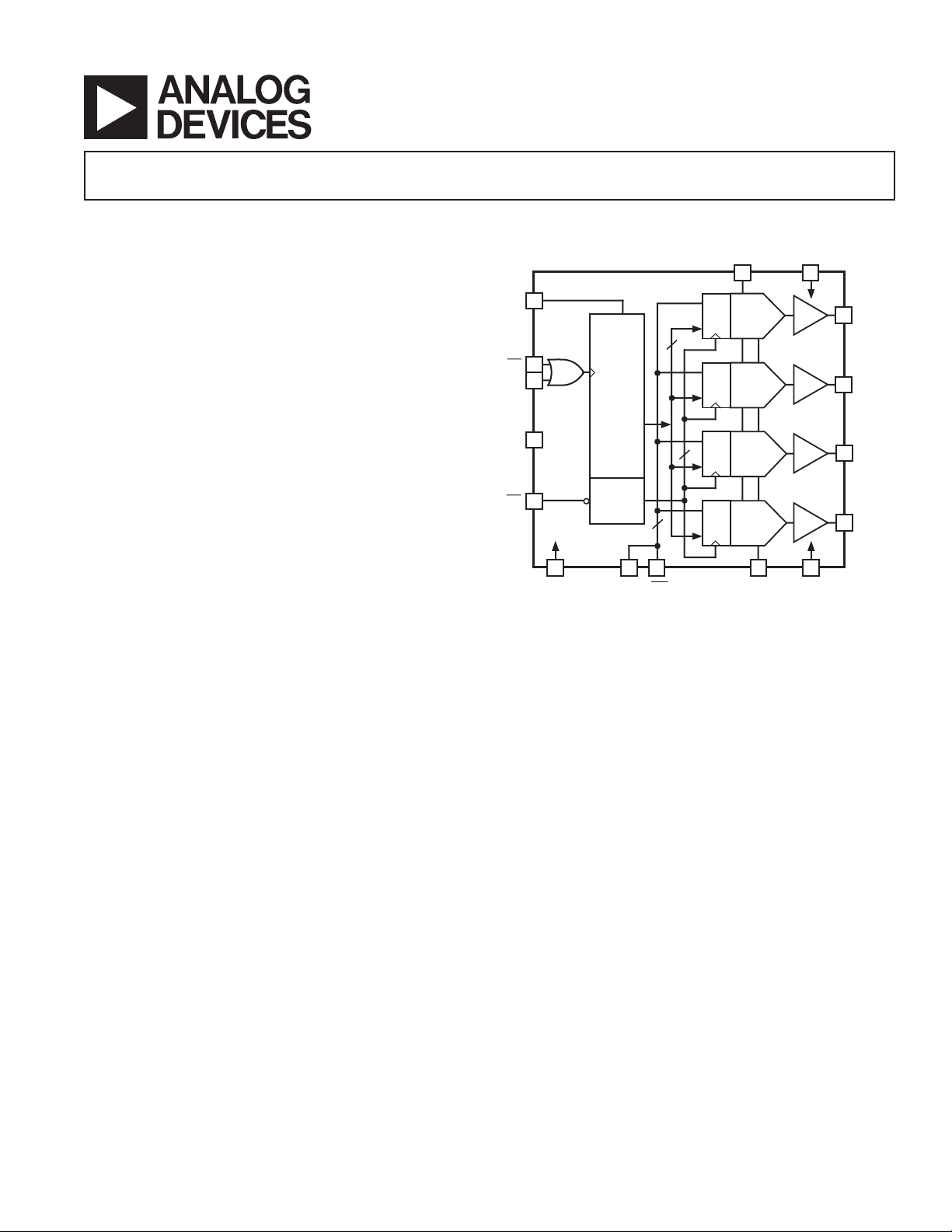
The DAC8420 is a quad, 12-bit voltage-output DAC with serial
digital interface in a 16-lead package. Utilizing BiCMOS technology, this monolithic device features unusually high circuit density
and low power consumption. The simple, easy-to-use serial digital
input and fully buffered analog voltage outputs require no external
components to achieve specified performance.
The 3-wire serial digital input is easily interfaced to microprocessors running at 10 MHz with minimal additional circuitry.
Each DAC is addressed individually by a 16-bit serial word
consisting of a 12-bit data word and an address header. The
user-programmable reset control CLR forces all four DAC
FUNCTIONAL BLOCK DIAGRAM
VDD
1
7
VOUTA
6
VOUTB
3
VOUTC
2
VOUTD
4
815169
SDI
CS
CLK
NC
LD
VREFHI
5
10
12
11
13
14
GND
SHIFT
REGISTER
DECODE
CLSEL
2
CLR
REG
REG
DAC A
A
A
12
REG
DAC B
B
REG
4
DAC C
C
REG
DAC D
D
VREFLO VSS
outputs to either zero scale or midscale, asynchronously overriding the current DAC register values. The output voltage range,
determined by the inputs VREFHI and VREFLO, is set by the
user for positive or negative unipolar or bipolar signal swings
within the supplies, allowing considerable design flexibility.
The DAC8420 is available in 16-lead PDIP, CERDIP, and
SOIC packages. Operation is specified with supplies ranging
from +5 V only to ±15 V, with references of +2.5 V to ±10 V,
respectively. Power dissipation when operating from ±15 V
supplies is less than 255 mW (max), and only 35 mW (max)
with a +5 V supply.
REV. A
Information furnished by Analog Devices is believed to be accurate and
reliable. However, no responsibility is assumed by Analog Devices for its
use, nor for any infringements of patents or other rights of third parties that
may result from its use. No license is granted by implication or otherwise
under any patent or patent rights of Analog Devices. Trademarks and
registered trademarks are the property of their respective owners.
One Technology Way, P.O. Box 9106, Norwood, MA 02062-9106, U.S.A.
Tel: 781/329-4700 www.analog.com
Fax: 781/326-8703 © 2003 Analog Devices, Inc. All rights reserved.
Page 2

DAC8420–SPECIFICATIONS
1
ELECTRICAL CHARACTERISTICS
VSS = –5.0 V ⴞ 5%, V
= –2.5 V, –40ⴗC ≤ TA ≤ +85ⴗC, unless otherwise noted. See Note 2 for supply variations.)
VREFLO
(@ VDD = +5.0 V ⴞ 5%, VSS = 0.0 V, V
= +2.5 V, V
VREFHI
= 0.0 V, and
VREFLD
Parameter Symbol Condition Min Typ Max Unit
STATIC ACCURACY
Integral Linearity E Grade INL ±1/4 ±1 LSB
Integral Linearity E Grade INL Note 3, V
= 0 V ±1/2 ±3 LSB
SS
Integral Linearity F Grade INL ± 3/4 ± 2 LSB
Integral Linearity F Grade INL Note 3, V
= 0 V ±1 ±4 LSB
SS
Differential Linearity DNL Monotonic over Temperature ±1/4 ±1 LSB
Zero-Scale Error ZSE R
Full-Scale Error FSE R
Zero-Scale Error ZSE Note 3, R
Full-Scale Error FSE Note 3, R
Zero-Scale Tempco TC
Full-Scale Tempco TC
ZSE
FSE
= 2 kΩ, VSS = –5 V ±4 LSB
L
= 2 kΩ, VSS = –5 V ±4 LSB
L
= 2 kΩ, VSS = 0 V ±8 LSB
L
= 2 kΩ, VSS = 0 V ±8 LSB
L
Note 4, RL = 2 kΩ, VSS = –5 V ±10 ppm/°C
Note 4, RL = 2 kΩ, VSS = –5 V ±10 ppm/°C
MATCHING PERFORMANCE
Linearity Matching ±1 LSB
REFERENCE
Positive Reference Input Range V
Negative Reference Input Range V
Negative Reference Input Range V
Reference High Input Current I
Reference Low Input Current I
VREFHI
VREFLO
VREFLO
VREFHI
VREFLO
Note 5 V
Note 5 V
Note 5, VSS = 0 V 0 V
Codes 0x000, 0x555 –0.75 ±0.25 +0.75 mA
Codes 0x000, 0x555, VSS = –5 V –1.0 –0.6 mA
+ 2.5 VDD – 2.5 V
VREFLO
SS
V
VREFHI
VREFHI
– 2.5 V
– 2.5 V
AMPLIFIER CHARACTERISTICS
Output Current I
Settling Time t
OUT
S
VSS = –5 V –1.25 +1.25 mA
To 0.01%, Note 6 8 µs
Slew Rate SR 10% to 90%, Note 6 1.5 V/µs
LOGIC CHARACTERISTICS
Logic Input High Voltage V
Logic Input Low Voltage V
Logic Input Current I
Input Capacitance C
LOGIC TIMING CHARACTERISTICS
Data Setup Time t
Data Hold t
Clock Pulse Width High t
Clock Pulse Width Low t
Select Time t
Deselect Delay t
Load Disable Time t
Load Delay t
Load Pulse Width t
Clear Pulse Width t
4, 7
INH
INL
IN
IN
DS
DH
CH
CL
CSS
CSH
LD1
LD2
LDW
CLRW
Note 4 13 pF
2.4 V
0.8 V
10 µA
25 ns
55 ns
90 ns
120 ns
90 ns
5ns
130 ns
35 ns
80 ns
150 ns
SUPPLY CHARACTERISTICS
Power Supply Sensitivity PSRR 0.002 0.01 %/%
Positive Supply Current I
Negative Supply Current I
Power Dissipation P
NOTES
1
Typical values indicate performance measured at 25°C.
2
All supplies can be varied ± 5% and operation is guaranteed. Device is tested with VDD = 4.75 V.
3
For single-supply operation (V
4
Guaranteed but not tested.
5
Operation is guaranteed over this reference range, but linearity is neither tested nor guaranteed.
6
V
swing between +2.5 V and –2.5 V with VDD = 5.0 V.
OUT
7
All input control signals are specified with tr = tf = 5 ns (10% to 90% of 5 V) and timed from a voltage level of 1.6 V.
Specifications subject to change without notice.
= 0 V, VSS = 0 V), due to internal offset errors INL and DNL are measured beginning at code 0x003.
VREFLO
DD
SS
DISS
–6 –3 mA
VSS = 0 V 20 35 mW
47 mA
REV. A–2–
Page 3

DAC8420
1
ELECTRICAL CHARACTERISTICS
V
= –10.0 V, –40ⴗC ≤ TA ≤ +85ⴗC, unless otherwise noted. See Note 2 for supply variations.)
VREFLO
(@ VDD = +15.0 V ⴞ 5%, VSS = –15.0 V ⴞ 5%, V
Parameter Symbol Condition Min Typ Max Unit
STATIC ACCURACY
Integral Linearity E Grade INL ±1/4 ±1/2 LSB
Integral Linearity F Grade INL ± 1/2 ± 1 LSB
Differential Linearity DNL Monotonic over Temperature ±1/4 ±1 LSB
Zero-Scale Error ZSE R
Full-Scale Error FSE R
Zero-Scale Tempco TC
Full-Scale Tempco TC
ZSE
FSE
= 2 kΩ±2 LSB
L
= 2 kΩ±2 LSB
L
Note 3, RL = 2 kΩ±4 ppm/°C
Note 3, RL = 2 kΩ±4 ppm/°C
MATCHING PERFORMANCE
Linearity Matching ±1 LSB
REFERENCE
Positive Reference Input Range V
Negative Reference Input Range V
Reference High Input Current I
Reference Low Input Current I
VREFHI
VREFLO
VREFHI
VREFLO
Note 4 V
Note 4 –10 V
Codes 0x000, 0x555 –2.0 ±1.0 +2.0 mA
Codes 0x000, 0x555 –3.5 –2.0 mA
AMPLIFIER CHARACTERISTICS
Output Current I
Settling Time t
OUT
S
To 0.01%, Note 5 13 µs
–5 +5 mA
Slew Rate SR 10% to 90%, Note 5 2 V/µs
= +10.0 V,
VREFHI
+ 2.5 VDD – 2.5 V
VREFLO
VREFHI
– 2.5 V
DYNAMIC PERFORMANCE
Analog Crosstalk Note 3 >64 dB
Digital Feedthrough Note 3 >72 dB
Large Signal Bandwidth 3 dB, V
V
VREFLO
= 5 V + 10 V p-p, 90 kHz
VREFHI
= –10 V, Note 3
Glitch Impulse Code Transition = 0x7FF to 0x800, Note 3 6 µV-s
LOGIC CHARACTERISTICS
Logic Input High Voltage V
Logic Input Low Voltage V
Logic Input Current I
Input Capacitance C
LOGIC TIMING CHARACTERISTICS
3, 6
Data Setup Time t
Data Hold t
Clock Pulse Width High t
Clock Pulse Width Low t
Select Time t
Deselect Delay t
Load Disable Time t
Load Delay t
Load Pulse Width t
Clear Pulse Width t
INH
INL
IN
IN
DS
DH
CH
CL
CSS
CSH
LD1
LD2
LDW
CLRW
Note 3 13 pF
2.4 V
0.8 V
10 µA
25 ns
20 ns
30 ns
50 ns
55 ns
15 ns
40 ns
15 ns
45 ns
70 ns
SUPPLY CHARACTERISTICS
Power Supply Sensitivity PSRR 0.002 0.01 %/%
Positive Supply Current I
Negative Supply Current I
Power Dissipation P
NOTES
1
Typical values indicate performance measured at 25°C.
2
All supplies can be varied ± 5% and operation is guaranteed.
3
Guaranteed but not tested.
4
Operation is guaranteed over this reference range, but linearity is neither tested nor guaranteed.
5
V
swing between +10 V and –10 V.
OUT
6
All input control signals are specified with tr = tf = 5 ns (10% to 90% of 5 V) and timed from a voltage level of 1.6 V.
Specifications subject to change without notice.
REV. A
DD
SS
DISS
–8 –5 mA
–3–
69 mA
255 mW
Page 4
DAC8420
ABSOLUTE MAXIMUM RATINGS
(TA = 25°C, unless otherwise noted.)
VDD to GND . . . . . . . . . . . . . . . . . . . . . . . . . –0.3 V, +18.0 V
to GND . . . . . . . . . . . . . . . . . . . . . . . . . . +0.3 V, –18.0 V
V
SS
V
to VDD . . . . . . . . . . . . . . . . . . . . . . . . . . . –0.3 V, +36.0 V
SS
V
to V
SS
V
VREFHI
V
VREFHI
I
, I
VREFHI
Digital Input Voltage to GND . . . . . . . . . –0.3 V, V
. . . . . . . . . . . . . . . . . . . . . . –0.3 V, VSS – 2.0 V
VREFLO
to V
. . . . . . . . . . . . . . . . . . . +2.0 V, VDD – V
VREFLO
SS
to VDD . . . . . . . . . . . . . . . . . . . . . . . +2.0 V, +33.0 V
. . . . . . . . . . . . . . . . . . . . . . . . . . . . . . . 10 mA
VREFLO
+ 0.3 V
DD
Output Short-Circuit Duration . . . . . . . . . . . . . . . . Indefinite
Operating Temperature Range
EP, FP, ES, FS, EQ, FQ . . . . . . . . . . . . . . –40°C to +85°C
Dice Junction Temperature . . . . . . . . . . . . . . . . . . . . . . 150°C
Storage Temperature . . . . . . . . . . . . . . . . . . –65°C to +150°C
Power Dissipation . . . . . . . . . . . . . . . . . . . . . . . . . . 1000 mW
Lead Temperature (Soldering, 60 sec) . . . . . . . . . . . . . 300°C
Thermal Resistance
Package Type θ
16-Lead Plastic DIP (P) 70
16-Lead Ceramic DIP (Q) 82
16-Lead Small Outline
Surface-Mount (S) 86
NOTES
1
θJA is specified for worst case mounting conditions, i.e., θJA is specified for
device in socket.
2
θJA is specified for device on board.
JA
1
1
2
θ
JC
Unit
27 °C/W
9 °C/W
22 °C/W
CAUTION
1. Stresses above those listed under Absolute Maximum Ratings
may cause permanent damage to the device. This is a stress
rating only and functional operation at or above this specification is not implied. Exposure to the above maximum rating
conditions for extended periods may affect device
reliability.
2. Digital inputs and outputs are protected; however, permanent
damage may occur on unprotected units from high energy
electrostatic fields. Keep units in conductive foam or packaging
at all times until ready to use. Use proper antistatic handling
procedures.
3. Remove power before inserting or removing units from their
sockets.
4. Analog outputs are protected from short circuits to ground or
either supply.
ORDERING GUIDE
Model Package Description Pin Count INL* (±LSB) Temperature Range
DAC8420EP Plastic/Epoxy DIP (PDIP) 16 0.5 –40°C to +85°C
DAC8420ES Standard Small Outline Package (SOIC) 16 0.5 –40°C to +85°C
DAC8420ES-REEL Standard Small Outline Package (SOIC) 16 0.5 –40°C to +85°C
DAC8420FP Plastic/Epoxy DIP (PDIP) 16 1.0 –40°C to +85°C
DAC8420FQ CERDIP Glass Seal 16 1.0 –40°C to +85°C
DAC8420FS Standard Small Outline Package (SOIC) 16 1.0 –40°C to +85°C
DAC8420FS-REEL Standard Small Outline Package (SOIC) 16 1.0 –40°C to +85°C
*INL measured at VDD = +15 V and VSS = –15 V.
CAUTION
ESD (electrostatic discharge) sensitive device. Electrostatic charges as high as 4000 V readily
accumulate on the human body and test equipment and can discharge without detection. Although the
DAC8420 features proprietary ESD protection circuitry, permanent damage may occur on devices
subjected to high energy electrostatic discharges. Therefore, proper ESD precautions are recommended
to avoid performance degradation or loss of functionality.
–4– REV. A
Page 5
DAC8420
DATA LOAD SEQUENCE
CS
SDI
CLK
LD
DATA LOAD TIMING
t
CSH
t
S
CS
A1 A0 X X D11 D10 D9 D8 D4 D3 D2 D1 D0
t
LD1
t
t
DH
DS
SDI
CLK
t
CL
CS
LD
V
OUT
t
CH
t
CSH
t
LD2
t
LDW
t
S
±1LSB
CLEAR TIMING
CLSEL
CLR
V
OUT
t
CLRW
t
S
t
LD2
±1LSB
+15V
1N4001
–10V
1N4001
+10V
1N4001
–15V
1N4001
Figure 1. Timing Diagram
10kΩ
+
10µF 0.1µF
10kΩ
10µF 0.1µF
+
10kΩ
+
10µF 0.1µF
NC
NC
5kΩ
NC
10kΩ
10µF 0.1µF
+
Figure 2. Burn-In Diagram
1
2
3
4
5
6
NC
7
8
NC = NO CONNECT
DUT
16
15
14
13
12
11
10
9
5kΩ
NC
10kΩ
REV. A
–5–
Page 6
DAC8420
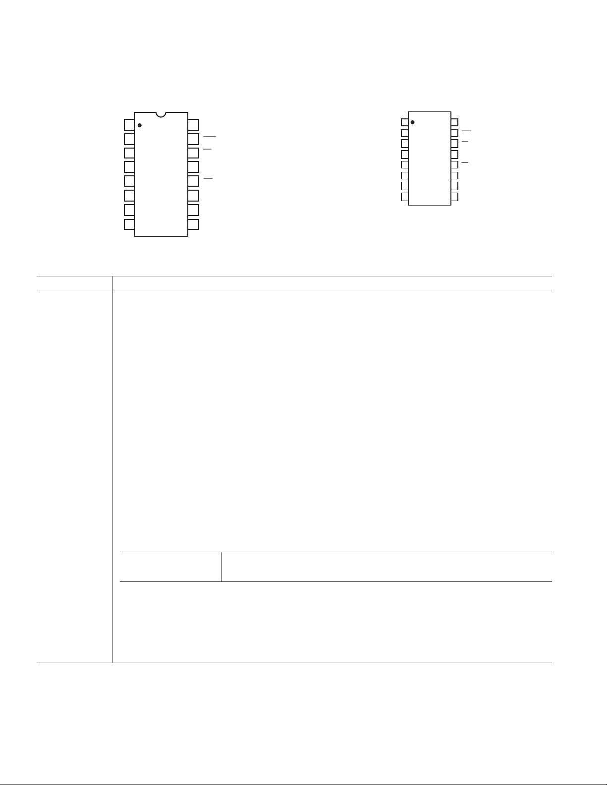
PDIP and CERDIP
PIN CONFIGURATIONS
SOIC
VDD
VOUTD
VOUTC
VREFLO
VREFHI
VOUTB
VOUTA
VSS
1
2
3
4
DAC8420
TOP VIEW
5
(Not to Scale)
6
7
8
NC = NO CONNECT
1
CLSEL
16
15
CLR
LD
14
13
NC
CS
12
CLK
11
SDI
10
9
GND
VDD
VOUTD
VOUTC
VREFLO
VREFHI
VOUTB
VOUTA
VSS
2
DAC-8420
TOP VIEW
3
DAC-8420
(Not to Scale)
DAC8420
4
TOP VIEW
TOP VIEW
5
(Not to Scale)
(Not to Scale)
6
7
8
NC = NO CONNECT
16
CLSEL
15
CLR
14
LD
13
NC
12
CS
11
CLK
10
SDI
9
GND
PIN FUNCTION DESCRIPTIONS
Mnemonic Description
Power Supplies VDD: Positive Supply, 5 V to 15 V.
VSS: Negative Supply, 0 V to –15 V.
GND: Digital Ground.
Clock CLK: System Serial Data Clock Input, TTL/CMOS Levels. Data presented to the input SDI is shifted into
the internal serial-parallel input register on the rising edge of clock. This input is logically ORed with CS.
Control Inputs (All are CMOS/TTL compatible.)
CLR: Asynchronous Clear, Active Low. Sets internal data registers A through D to zero or midscale, depending on current state of CLSEL. The data in the serial input shift register is unaffected by this control.
CLSEL: Determines action of CLR. If High, a clear command will set the internal DAC registers A through D
to midscale (0x800). If low, the registers are set to zero (0x000).
CS: Device Chip Select, Active low. This input is logically ORed with the clock and disables the serial data
register input when high. When low, data input clocking is enabled. See Table I.
LD: Asynchronous DAC Register Load Control, Active Low. The data currently contained in the serial input
shift register is shifted out to the DAC data registers on the falling edge of LD, independent of CS. Input data
must remain stable while LD is low.
Data Input (All are CMOS/TTL compatible.)
SDI: Serial Data Input. Data presented to this pin is loaded into the internal serial-parallel shift register, which
shifts data in beginning with DAC address Bit A1. This input is ignored when CS is high.
The format of the 16-bit serial word is
(FIRST) (LAST)
B0 B1 B2 B3 B4 B5 B6 B7 B8 B9 B10 B11 B12 B13 B14 B15
A1 A0 NC NC D11 D10 D9 D8 D7 D6 D5 D4 D3 D2 D1 D0
—Address Word— (MSB) —DAC Data-Word— (LSB)
NC = Don’t Care.
Reference Inputs VREFHI: Upper DAC ladder reference voltage input. Allowable range is (VDD – 2.5 V) to (V
VREFLO: Lower DAC ladder reference voltage input, equal to zero-scale output. Allowable range is V
(V
VREFHI
– 2.5 V).
VREFLO
+ 2.5 V).
to
SS
Analog Outputs VOUTA through VOUTD: Four buffered DAC voltage outputs.
–6– REV. A
Page 7

DAC8420
Table I. Control Function Logic Table
1
CLK
NC H H L H No Change Loads Midscale Value (0x800)
NC H H L L No Change Loads Zero-Scale Value (0x000)
NC H H ↑ H/L No Change Latches Value
↑ L HHNCShifts Register One Bit No Change
L ↑ HHNCShifts Register One Bit No Change
H NC (↑) ↓ HNCNo Change Loads the Serial Data-Word
HNCL HNCNo Change Transparent
NC H H H NC No Change No Change
NC = Don’t Care.
NOTES
1
CS and CLK are interchangeable.
2
Returning CS high while CLK is high avoids an additional false clock of serial input data. See Note 1.
3
Do not clock in serial data while LD is low.
OPERATION
Introduction
The DAC8420 is a quad, voltage-output 12-bit DAC with
serial digital input capable of operating from a single 5 V supply.
The straightforward serial interface can be connected directly to
most popular microprocessors and microcontrollers, and can
accept data at a 10 MHz clock rate when operating from ±15 V
supplies. A unique voltage reference structure ensures maximum utilization of DAC output resolution by allowing the user
to set the zero-scale and full-scale output levels within the supply rails. The analog voltage outputs are fully buffered, and are
capable of driving a 2 kΩ load. Output glitch impulse during
major code transitions is a very low 64 nV-s (typ).
Digital Interface Operation
The serial input of the DAC-8420, consisting of CS, SDI,
and LD, is easily interfaced to a wide variety of microprocessor
serial ports. As shown in Table I and in the timing diagram
(Figure 1), while CS is low the data presented to the input SDI
is shifted into the internal serial/parallel shift register on the
rising edge of the clock, with the address MSB first, data LSB
last. The data format, shown above, is two bits of DAC address
and two “don’t care” fill bits, followed by the 12-bit DAC dataword. Once all 16 bits of the serial data-word have been input,
the load control LD is strobed and the word is parallel-shifted
out onto the internal data bus. The two address bits are
decoded and used to route the 12-bit data-word to the appropriate DAC data register. See the Applications section.
Correct Operation of CS and CLK
As mentioned in Table I, the control pins CLK and CS require
some attention during a data load cycle. Since these two inputs
are fed to the same logical OR gate, the operation is in fact
identical. The user must take care to operate them accordingly
in order to avoid clocking in false data bits. As shown in the
timing diagram, CLK must be halted high or CS must be
brought high during the last high portion of the CLK following
the rising edge that latched in the last data bit. Otherwise, an
additional rising edge is generated by CS rising while CLK is
low, causing CS to act as the clock and allowing a false data bit
into the serial input register. The same issue must also be considered in the beginning of the data load sequence.
Using CLR and CLSEL
The CLEAR (CLR) control allows the user to perform an asynchronous reset function. Asserting CLR loads all four DAC
data- word registers, forcing the DAC outputs to either
CS
1
LD CLR CLSEL Serial Input Shift Register DAC Registers A–D
2
3
zero-scale (0x000) or midscale (0x800), depending on the state
of CLSEL as shown in Table I. The CLEAR function is asynchronous and totally independent of CS. When CLR returns
high, the DAC outputs remain latched at the reset value until
LD is strobed, reloading the individual DAC data-word registers with either the data held in the serial input register prior to
the reset or with new data loaded through the serial interface.
Table II. DAC Address Word Decode Table
A1 A0 DAC Addressed
00DAC A
01DAC B
10DAC C
11DAC D
Programming the Analog Outputs
The unique differential reference structure of the DAC8420
allows the user to tailor the output voltage range precisely to
the needs of the application. Instead of spending DAC resolution on an unused region near the positive or negative rail,
the DAC8420 allows the user to determine both the upper
and lower limits of the analog output voltage range. Thus, as
shown in Table III and Figure 3, the outputs of DACs A
through D range between VREFHI and VREFLO, within the
limits specified in the Specifications section. Note also that
VREFHI must be greater than VREFLO.
V
DD
2.5V MIN
V
SS
2.5V MIN
0xFFF
1 LSB
0x000
–10V MIN
0V MIN
V
VREFHI
V
VREFLO
Figure 3. Output Voltage Range Programming
REV. A
–7–
Page 8

DAC8420
Table III. Analog Output Code
DAC Data-Word (Hex) V
0xFFF
0x801
0x800
0x7FF
0x000
OUT
VREFLO +
VREFLO +
VREFLO +
VREFLO +
VREFLO +
(VREFHI – VREFLO )
4096
(VREFHI – VREFLO )
4096
(VREFHI – VREFLO )
4096
(VREFHI – VREFLO )
4096
(VREFHI – VREFLO )
4096
× 4095
× 2049
× 2048
× 2047
× 0
Note
Full-Scale Output
Midscale + 1
Midscale
Midscale – 1
Zero-Scale
–8– REV. A
Page 9

Typical Performance Characteristics–DAC8420
0.3
0.2
0.1
0
DNL – LSB
–0.1
–0.2
–0.3
–4
–6
TA = +25°C
V
= +15V, V
DD
V
VREFLO
V
VREFHI
= –10V
– V
TPC 1. Differential Linearity vs.
±
1.5
15 V)
TA = +25ⴗC
V
V
V
VREFHI
= +5V, V
DD
VREFLO
– V
VREFHI (
0.4
0.3
0.2
0.1
0
INL – LSB
–0.1
–0.2
–0.3
–0.4
TPC 4. INL vs. VREFHI (+5 V)
SS
= 0V
= –15V
= 0V
SS
3.53.02.52.0
0.10
V
VREFHI
TA = +25°C
V
V
= +5V, VSS = 0V
DD
= 0V
VREFLO
– V
3.53.02.52.0
0.05
0
–0.05
–0.10
DNL – LSB
–0.15
–0.20
–0.25
121086420–2
14
–0.30
1.5
TPC 2. Differential Linearity vs.
0.3
0.2
0.1
0
INL – LSB
–0.1
–0.2
–0.3
–4
–6
TA = +25°C
V
DD
V
VREFLO
V
VREFHI
= +15V, V
– V
TPC 3. INL vs. VREFHI (±15 V)
= –10V
SS
= –15V
121086420–2
14
VREFHI (+5 V)
0.7
0.5
= 2k⍀ – LSB
L
0.3
0.1
–0.1
–0.3
FULL-SCALE ERROR WITH R
–0.5
0 200 400
VDD = +15V, VSS = –15V
= +10V
V
VREFHI
= –10V
V
VREFLO
T = HOURS OF OPERATION AT 125ⴗC
CURVES NOT NORMALIZED
600 800 1000
TPC 5. Full-Scale Error vs.
Time Accelerated by Burn-In
x + 3
x
x – 3
1.2
1.0
VDD = +15V, VSS = –15V
= +10V
V
VREFHI
= –10V
V
VREFLO
T = HOURS OF OPERATION AT 125ⴗC
CURVES NOT NORMALIZED
600 800 1000
= 2k⍀ – LSB
L
0.8
0.6
0.4
0.2
FULL-SCALE ERROR WITH R
0
0 200 400
TPC 6. Zero-Scale Error vs.
Time Accelerated by Burn-In
x + 3
x
x – 3
0.2
V
0.1
–0.1
–0.2
–0.3
–0.4
FULL-SCALE ERROR – LSB
–0.5
–0.6
= +15V, V
DD
V
VREFHI
V
0
VREFLO
–50–75
= –15V
SS
= +10V
= –10V
DAC C
TEMPERATURE – °C
TPC 7. Full-Scale Error vs.
Temperature
REV. A
DAC D
DAC B
DAC A
1007550250–25
125
1.2
V
1.0
0.8
0.6
RROR – LSB
0.4
0.2
0
ZERO-SCALE E
–0.2
–0.4
DD
V
VREFHI
V
VREFLO
DAC A
–50–75
= +15V, V
= –15V
SS
= +10V
= –10V
DAC B
TEMPERATURE – ⴗC
TPC 8. Zero-Scale Error vs.
Temperature
–9–
DAC C
DAC D
1007550250–25
125
ERROR – ⴞLSB
0.9
0.7
0.5
0.3
0.1
–0.1
–0.3
–0.5
–0.7
–0.9
5000
TA = +25ⴗC
V
= +15V, V
DD
V
= +10V
VREFHI
V
= –10V
VREFLO
DIGITAL INPUT CODE
TPC 9. Channel-to-Channel
±
Matching
15/±10
SS
= –15V
4000350030002500200015001000
4500
Page 10

DAC8420
/
+1.5
+1.0
+0.5
TA = +25ⴗC
V
V
V
0
ERROR – LSB
–0.5
–1.0
–1.5
500
0
DIGITAL INPUT CODE
TPC 10. Channel-to-Channel
Matching +5/+2.5
1.5
1.0
0.5
– mA
VREFHI
I
–0.5
–1.0
TA = +25ⴗC
V
= +15V, V
DD
V
= +10V
VREFHI
V
= –10V
VREFLO
50000
DIGITAL INPUT CODE
TPC 13. I
= –15V
SS
VREFHI
vs. Code
= +5V, V
DD
VREFHI
VREFLO
SS
= +2.5V
= 0V
= 0V
4000350030002500200015001000
4000350030002500200015001000
4500
13
12
11
TA = +25ⴗC
V
= +15V, V
DD
V
VREFLO
10
9
– mA
8
DD
I
7
6
5
4
–5–7
TPC 11. IDD vs. V
0
V
VREFHI
VREFHI
DACs High
–250V
LD
1.22mV
1 LSB
0mV
TA = +25ⴗC
= +5V, V
V
DD
V
VREFHI
V
VREFLO
–10.25mV
t
8s
SETT
TPC 14. Settling Time (+)(±5 V)
= –10V
– V
, All
= +2.5V
= –2.5V
SS
SS
= –15V
= –5V
0.8
0.7
0.6
0.5
0.4
TA = +25, –55, 125ⴗC
V
DD
V
VREFHI
V
VREFLO
= +15V, V
= +10V
= –10V
SS
= –15V
0.3
0.2
0.1
INL – LSB
0
–0.1
–0.2
–0.3
–0.4
13
1197531–1–3
5000
DIGITAL INPUT CODE
3500 400030002500200015001000
4500
TPC 12. INL vs. Code ±15/±10
6.5mV
CLR
TA = +25ⴗC
V
= +5V, V
DD
V
VREFHI
V
VREFLO
0mV
1 LSB
–1.22mV
45.1s–4.9s5s/DIV
–3.5mV
t
SETT
8s
SS
= +2.5V
= –2.5V
= –5V
+45.1s–4.9s+5s/DIV
TPC 15. Settling Time (–)(±5 V)
+31.25mV
LD
TA = +25ⴗC
V
= +15V, V
DD
V
VREFHI
V
VREFLO
= +10V
= –10V
SS
= –15V
+43.75mV
CLR
TA = +25ⴗC
V
= +15V, V
DD
V
VREFHI
V
VREFLO
= +10V
= –10V
SS
= –15V
+5V
+1V
DIV
0
4.88mV
1 LSB
0mV
–18.75mV
–9.8s
t
SETT
+10s/DIV
13s
TPC 16. Settling Time (+)(±15 V)
+90.2s
0mV
1 LSB
–4.88mV
–6.25mV
13s
t
SETT
TPC 17. Settling Time (–)(±15 V)
+90.2s–9.8s +10s/DIV
–5V
TPC 18. Slew Rate (±5 V)
SR
= 1.65 SR
RISE
TA = +25ⴗC
V
= +5V, V
DD
V
VREFHI
V
VREFLO
20s/DIV
V
s
SS
= +2.5V
= –2.5V
= –5V
FALL
= 1.17
152.4s–47.6s
V
s
REV. A–10–
Page 11

DAC8420
k
+25V
LD
CLR
+5V
/DIV
0
TA = +25ⴗC
V
–25V
DD
V
VREFHI
SR
= +15V, V
RISE
SS
= +10V, V
= 1.9
= –15V
VREFLO
20s/DIV
V
s
TPC 19. Slew Rate (±15 V)
6
4
2
V
= +15V
DD
V
= –15V
SS
0
V
= +10V
VREFHI
= –10V
V
VREFLO
ALL DACS HIGH (FULL SCALE)
–2
–4
POWER SUPPLY CURRENT – mA
–6
–75
TEMPERATURE – ⴗC
100
90
10
0
–10
–20
GAIN – dB
–30
TA = +25ⴗC
V
= +15V, V
DD
V
VREFHI
V
VREFLO
= –10V
166.4s–33.6s
= 2.02
V
s
SR
FALL
ALL BITS HIGH 200mV p-p
10 100 10M1M100k10k1k
= –15V
SS
= 0 ⴞ 100mV
= –10V
FREQUENCY – Hz
TPC 20. Small-Signal Response
I
DD
I
SS
750
150
V
TA = +25 C
V
V
V
V
DATA = 0x800
10mA/DIV
THROUGH V
OUTA
= +15V
DD
= –15V
SS
VREFHI
VREFLO
= +10V
= –10V
OUTD
5V/DIV
80
70
60
50
40
PSRR – dB
30
TA = +25 C
20
DATA = 0x000
V
10
0
= +15V ⴞ1V, V
DD
V
= +10V
VREFHI
V
= –10V
VREFLO
10
100 1k 10k 100k 1M
= –15V
SS
FREQUENCY – Hz
TPC 21. PSRR vs. Frequency
10
8
6
PEAK – V
4
OUT
V
2
0
10 100 10
TA = +25 C
V
= +15V
DD
= –15V
V
SS
= +10V
V
VREFHI
V
= –10V
VREFLO
DATA = 0xFFF OR 0x000
LOAD RESISTANCE – ⍀
1k
TPC 22. Power Supply Current
vs. Temperature
TPC 23. DAC Output Current vs.
VOUTX
TPC 24. Output Swing vs.
Load Resistance
REV. A
–11–
Page 12

DAC8420
VREFHI Input Requirements
The DAC8420 utilizes a unique, patented DAC switch driver
circuit that compensates for different supply, reference voltage, and digital code inputs. This ensures that all DAC ladder
switches are always biased equally, ensuring excellent linearity
under all conditions. Thus, as indicated in the specifications,
the VREFHI input of the DAC8420 requires both sourcing
and sinking current capability from the reference voltage
source. Many positive voltage references are intended as
current sources only and offer little sinking capability. The
user should consider references such as the AD584, AD586,
AD587, AD588, AD780, and REF43 for such an application.
Power-Up Sequence
To prevent CMOS latch-up condition, powering VDD, VSS,
and GND prior to any reference voltages is recommended. The
ideal power-up sequence is GND, VSS, VDD, VREFHI,
VREFLO, and digital inputs. Noncompliance with the powerup sequence over an extended period can elevate the reference
currents and eventually damage the device. On the other
hand, if the noncompliant power-up sequence condition is as
short as a few milliseconds, the device can resume normal
operation without being damaged once V
DD/VSS
is powered.
APPLICATIONS
Power Supply Bypassing and Grounding
In any circuit where accuracy is important, careful consideration
of the power supply and ground return layout helps to ensure
the rated performance. The DAC8420 has a single ground pin
that is internally connected to the digital section as the logic
reference level. The first thought may be to connect this pin to
the digital ground; however, in large systems the digital ground
is often noisy because of the switching currents of other digital
circuitry. Any noise that is introduced at the ground pin could
couple into the analog output. Thus, to avoid error-causing
digital noise in the sensitive analog circuitry, the ground pin
should be connected to the system analog ground. The ground
path (circuit board trace) should be as wide as possible to reduce
any effects of parasitic inductance and ohmic drops. A ground
plane is recommended if possible. The noise immunity of the
on-board digital circuitry, typically in the hundreds of millivolts,
is well able to reject the common-mode noise typically seen
between system analog and digital grounds. Finally, the analog
and digital ground should be connected to each other at a single
point in the system to provide a common reference. This is
preferably done at the power supply.
Good grounding practice is essential to maintaining analog
performance in the surrounding analog support circuitry as well.
With two reference inputs, and four analog outputs capable of
moderate bandwidth and output current, there is a significant
potential for ground loops. Again, a ground plane is recommended as the most effective solution to minimizing errors due
to noise and ground offsets.
+V
S
10F
–V
S
0.1F
0.1F10F
1
VDD
8
VSS
10F = TANTALUM
0.1F = CERAMIC
GND
9
Figure 4. Recommended Supply Bypassing Scheme
The DAC8420 should have ample supply bypassing, located as
close to the package as possible. Figure 4 shows the recommended capacitor values of 10 µF in parallel with 0.1 µF. The
0.1 µF capacitor should have low effective series resistance
(ESR) and effective series inductance (ESI), such as the common ceramic types, which provide a low impedance path to
ground at high frequencies to handle transient currents due to
internal logic switching. In order to preserve the specified analog performance of the device, the supply should be as noise free
as possible. In the case of 5 V only systems, it is desirable to use
the same 5 V supply for both the analog circuitry and the digital
portion of the circuit. Unfortunately, the typical 5 V supply is
extremely noisy due to the fast edge rates of the popular CMOS
logic families, which induce large inductive voltage spikes, and
busy microcontroller or microprocessor buses, which commonly
have large current spikes during bus activity. However, by properly filtering the supply as shown in Figure 5, the digital 5 V
supply can be used. The inductors and capacitors generate a
filter that not only rejects noise due to the digital circuitry, but
also filters out the lower frequency noise of switch mode power
supplies. The analog supply should be connected as close as
possible to the origin of the digital supply to minimize noise
pickup from the digital section.
FERRITE BEADS:
2 TURNS, FAIR-RITE
TTL/CMOS
LOGIC
CIRCUITS
+5V
POWER SUPPLY
#2677006301
100F
ELECT.
10–22F
TANT.
+5V
0.1F
CER.
+5V
RETURN
Figure 5. Single-Supply Analog Supply Filter
–12– REV. A
Page 13

DAC8420
Analog Outputs
The DAC8420 features buffered analog voltage outputs capable
of sourcing and sinking up to 5 mA when operating from ±15 V
supplies, eliminating the need for external buffer amplifiers in
most applications while maintaining specified accuracy over the
rated operating conditions. The buffered outputs are simply an
op amp connected as a voltage follower, and thus have output
characteristics very similar to the typical operational amplifier.
These amplifiers are short-circuit protected. The designer
should verify that the output load meets the capabilities of
the device, in terms of both output current and load capacitance. The DAC8420 is stable with capacitive loads up to 2 nF
typical. However, any capacitive load will increase the settling
time, and should be minimized if speed is a concern.
The output stage includes a p-channel MOSFET to pull the
output voltage down to the negative supply. This is very important in single-supply systems where VREFLO usually has the same
potential as the negative supply. With no load, the zero-scale output voltage in these applications will be less than 500 µV typically,
or less than 1 LSB when V
= 2.5 V. However, when sinking
VREFHI
current, this voltage does increase because of the finite impedance
of the output stage. The effective value of the pull-down resistor in
the output stage is typically 320 Ω. With a 100 kΩ resistor connected to 5 V, the resulting zero-scale output voltage is 16 mV.
Thus, the best single-supply operation is obtained with the output
load connected to ground, so the output stage does not have to
sink current.
Like all amplifiers, the DAC8420 output buffers do generate
voltage noise, 52 nV/√Hz typically. This is easily reduced by
adding a simple RC low-pass filter on each output.
Reference Configuration
The two reference inputs of the DAC8420 allow a great deal of
flexibility in circuit design. The user must take care, however, to
observe the minimum voltage input levels on VREFHI and
VREFLO to maintain the accuracy shown in the data sheet.
These input voltages can be set anywhere across a wide range
within the supplies, but must be a minimum of 2.5 V apart in
any case. See Figure 3. A wide output voltage range can be
obtained with ±5 V references, which can be provided by the
AD588 as shown in Figure 6. Many applications utilize the
DACs to synthesize symmetric bipolar waveforms, which
requires an accurate, low drift bipolar reference. The AD588
provides both voltages and needs no external components.
Additionally, the part is trimmed in production for 12-bit accuracy over the full temperature range without user calibration.
Performing a Clear with the reset select CLSEL high allows the
user to easily reset the DAC outputs to midscale, or 0 V in these
applications.
When driving the reference inputs VREFHI and VREFLO, it is
important to note that VREFHI both sinks and sources current,
and that the input currents of both are code dependent. Many
voltage reference products have limited current sinking capability and must be buffered with an amplifier to drive VREFHI in
order to maintain overall system accuracy. The input VREFLO,
however, has no such requirement.
+15V SUPPLY
1F
V
GND
+5V
DAC A
DAC B
DAC C
DAC D
REFHI
49
V
REFLO
–5V
15
8
–15V SUPPLY
7
7
R
B
A1
R2
R3
A2
6
5
9
6
4 3
A3
1
AD588
R1
10
R4
R5
8 12
R6
11
13
14
15
A4
+V
2
S
0.1F
–V
16
S
0.1F
+5V
–5V
+15V
SUPPLY
SYSTEM
GROUND
–15V
SUPPLY
DAC8420
DIGITAL
CONTROL
15 1614121110
DIGITAL INPUTS
0.1F
VOUTA
7
VOUTB
6
VOUTC
3
VOUTD
2
0.1F
Figure 6.±10 V Bipolar Reference Configuration Using the AD588
REV. A
–13–
Page 14

DAC8420
For a single 5 V supply, V
is limited to at most 2.5 V, and
VREFHI
must always be at least 2.5 V less than the positive supply to
ensure linearity of the device. For these applications, the REF43
is an excellent low drift 2.5 V reference that consumes only
450 µA (max). It works well with the DAC8420 in a single 5 V
system as shown in Figure 7.
+5V SUPPLY
0.1F
REF43
VIN
2
4
DAC8420
DIGITAL
CONTROL
DIGITAL INPUTS
2.5V
6
VOUTGND
15 1614121110
9
GND
VREFHI
5
DAC A
DAC B
DAC C
DAC D
4
VREFLO
+5V SUPPLY
1
8
0.1F
VOUTA
7
VOUTB
6
VOUTC
3
VOUTD
2
Figure 7. 5 V Single-Supply Operation Using REF43
Isolated Digital Interface
Because the DAC8420 is ideal for generating accurate voltages
in process control and industrial applications, due to noise,
safety requirements, or distance, it may be necessary to isolate it
from the central controller. This can be easily achieved by using
opto-isolators, which are commonly used to provide electrical
isolation in excess of 3 kV. Figure 8 shows a simple 3-wire
interface scheme for controlling the clock, data, and load pulse.
For normal operation, CS is tied permanently low so that the
DAC8420 is always selected. The resistor and capacitor on the
CLR pin provide a power-on reset with 10 ms time constant. The
three opto-isolators are used for the SDI, CLK, and LD lines.
One opto-isolated line (LD) can be eliminated from this circuit
by adding an inexpensive 4-bit TTL counter to generate the
load pulse for the DAC8420 after 16 clock cycles. The counter
is used to count of the number of clock cycles loading serial data to
the DAC8420. After all 16 bits have been clocked into the converter, the counter resets, and a load pulse is generated on clock
17. In either circuit, the DAC8420’s serial interface provides a
simple, low cost method of isolating the digital control.
HIGH VOLTAGE
ISOLATION
POWER
5V
10k⍀
LD
5V
10k⍀
SCLK
5V
10k⍀
SDI
5V
REG
+5V
2
4
10k⍀
0.1F
5V
REF43
VIN
VOUT
GND
6
VREFHI
15
CLR
16
CLSEL
14
LD
CS
12
11
CLK
10
SDI
VREFLO
2.5V
5
DAC8420
VSS
4
8
5V
1
VDD
GND
0.1F
VOUTA
7
VOUTB
6
VOUTC
3
VOUTD
2
9
Figure 8. Opto-lsolated 3-Wire Interface
Dual Window Comparator
Often a comparator is needed to signal an out-of-range warning.
Combining the DAC8420 with a quad comparator such as the
CMP04 provides a simple dual window comparator with adjustable trip points as shown in Figure 9. This circuit can be
operated with either a dual-supply or a single-supply. For the A
input channel, DAC B sets the low trip point, and DAC A sets
the upper trip point. The CMP04 has open-collector outputs
that are connected together in wired-OR configuration to generate an out-of-range signal. For example, when VINA goes below
the trip point set by DAC B, comparator C2 pulls the output
down, turning on the red LED. The output can also be used as
a logic signal for further processing.
–14– REV. A
Page 15

DAC8420
5V SUPPLY
0.1F
REF43
VIN
2
4
GND
DAC8420
DIGITAL
CONTROL
DIGITAL INPUTS
VINA
5V SUPPLY
2.5V
6
V
OUT
VREFHI
5
DAC A
DAC B
DAC C
DAC D
15 1614121110
49
GND
VREFLO
1
8
VSS
0.1F
VOUTA
7
VOUTB
6
VOUTC
3
VOUTD
2
VINB
5V
0.1F
3
CMP04
5
C1
4
7
C2
6
9
C3
8
11
C4
10
2
1
14
13
12
5V
604⍀
RED LED
OUT A
5V
604⍀
RED LED
OUT B
Figure 9. Dual Programmable Window Comparator
MC68HC11 Microcontroller Interfacing
Figure 10 shows a serial interface between the DAC8420 and
the MC68HC11 8-bit microcontroller. The SCK output of the
MC68HC11 drives the CLK input of the DAC, and the MOSI
port outputs the serial data to load into the SDI input of the
DAC. The port lines PD5, PC0, PC1, and PC2 provide the
controls to the DAC as shown.
PC2
PC1
PC0
MC68HC11*
(PD5) SS
SCK
MOSI
*ADDITIONAL PINS OMITTED FOR CLARITY
CLSEL
CLR
CS
DAC8420*
LD
CLK
SDI
Figure 10. MC68HC11 Microcontroller Interface
For correct operation, the MC68HC11 should be configured
such that its CPOL bit and CPHA bit are both set to 1. In this
configuration, serial data on MOSI of the MC68HC11 is valid
on the rising edge of the clock, which is the required timing for
the DAC8420. Data is transmitted in 8-bit bytes (MSB first),
with only eight rising clock edges occurring in the transmit
cycle. To load data to the DAC8420’s input register, PC0 is
taken low and held low during the entire loading cycle. The first
eight bits are shifted in address first, immediately followed by
another eight bits in the second least-significant byte to load
the complete 16-bit word. At the end of the second byte load,
PC0 is then taken high. To prevent an additional advancing of
the internal shift register, SCK must already be asserted before
PC0 is taken high. To transfer the contents of the input shift
register to the DAC register, PD5 is then taken low, asserting
the LD input of the DAC and completing the loading process.
PD5 should return high before the next load cycle begins.
The DAC8420’s CLR input, controlled by the output PC1,
provides an asynchronous clear function.
REV. A
–15–
Page 16

DAC8420
DAC8420 to M68HC11 Interface Assembly Program
* M68HC11 Register Definitions
PORTC EQU $1003 Port C control register
* “0,0,0,0;0,CLSEL,CLR,CS”
DDRC EQU $1007 Port C data direction
PORTD EQU $1008 Port D data register
* “0,0,LD,SCLK;SDI,0,0,0”
DDRD EQU $1009 Port D data direction
SPCR EQU $1028 SPI control register
* “SPIE,SPE,DWOM,MSTR;CPOL,CPHA,SPR1,SPR0”
SPSR EQU $1029 SPI status register
* “SPIF,WCOL,0,MODF;0,0,0,0”
SPDR EQU $102A SPI data register; Read-Buffer; Write-Shifter
*
* SDI RAM variables: SDI1 is encoded from 0 (Hex) to CF (Hex)
* To select: DAC A – Set SDI1 to $0X
DAC B – Set SDI1 to $4X
DAC C – Set SDI1 to $8X
DAC D – Set SDI1 to $CX
SDI2 is encoded from 00 (Hex) to FF (Hex)
* DAC requires two 8-bit loads – Address + 12 bits
SDI1 EQU $00 SDI packed byte 1 “A1,A0,0,0;MSB,DB10,DB9,DB8”
SDI2 EQU $01 SDI packed byte 2
“DB7,DB6,DB5,DB4;DB3,DB2,DB1,DB0”
* Main Program
ORG $C000 Start of user’s RAM in EVB
INIT LDS #$CFFF Top of C page RAM
* Initialize Port C Outputs
LDAA #$07 0,0,0,0;0,1,1,1
* CLSEL-Hi, CLR-Hi, CS-Hi
* To reset DAC to ZERO-SCALE, set CLSEL-Lo ($03)
* To reset DAC to MID-SCALE, set CLSEL-Hi ($07)
STAA PORTC Initialize Port C Outputs
LDAA #$07 0,0,0,0;0,1,1,1
STAA DDRC CLSEL, CLR, and CS are now enabled as outputs
* Initialize Port D Outputs
LDAA #$30 0,0,1,1;0,0,0,0
* LD-Hi,SCLK-Hi,SDI-Lo
STAA PORTD Initialize Port D Outputs
LDAA #$38 0,0,1,1;1,0,0,0
STAA DDRD LD,SCLK, and SDI are now enabled as outputs
* Initialize SPI Interface
LDAA #$5F
STAA SPCR SPI is Master,CPHA=1,CPOL=1,Clk rate=E/32
* Call update subroutine
BSR UPDATE Xfer 2 8-bit words to DAC-8420
JMP $E000 Restart BUFFALO
* Subroutine UPDATE
UPDATE PSHX Save registers X, Y, and A
PSHY
PSHA
* Enter Contents of SDI1 Data Register (DAC# and 4 MSBs)
LDAA #$80 1,0,0,0;0,0,0,0
STAA SDI1 SDI1 is set to 80 (Hex)
* Enter Contents of SDI2 Data Register
LDAA #$00 0,0,0,0;0,0,0,0
STAA SDI2 SDI2 is set to 00 (Hex)
LDX #SDI1 Stack pointer at 1st byte to send via SDI
LDY #$1000 Stack pointer at on-chip registers
* Clear DAC output to zero
BCLR PORTC,Y $02 Assert CLR
BSET PORTC,Y $02 Deassert CLR
* Get DAC ready for data input
BCLR PORTC,Y $01 Assert CS
TFRLP LDAA 0,X Get a byte to transfer via SPI
STAA SPDR Write SDI data reg to start xfer
WAIT LDAA SPSR Loop to wait for SPIF
BPL WAIT SPIF is the MSB of SPSR
* (when SPIF is set, SPSR is negated)
INX Increment counter to next byte for xfer
CPX #SDI2+ 1 Are we done yet ?
BNE TFRLP If not, xfer the second byte
* Update DAC output with contents of DAC register
BCLR PORTD,Y 520 Assert LD
BSET PORTD,Y $20 Latch DAC register
BSET PORTC,Y $01 De-assert CS
PULA When done, restore registers X, Y & A
PULY
PULX
RTS ** Return to Main Program **
–16– REV. A
Page 17

OUTLINE DIMENSIONS
DAC8420
16-Lead Plastic Dual In-Line Package [PDIP]
Narrow Body (N-16)
P Suffix
Dimensions shown in inches and (millimeters)
0.785 (19.94)
0.765 (19.43)
0.745 (18.92)
16
1
0.100 (2.54)
BSC
0.015 (0.38)
0.180 (4.57)
MAX
0.150 (3.81)
0.130 (3.30)
0.110 (2.79)
0.022 (0.56)
0.018 (0.46)
0.014 (0.36)
CONTROLLING DIMENSIONS ARE IN INCHES; MILLIMETER DIMENSIONS
(IN PARENTHESES) ARE ROUNDED-OFF INCH EQUIVALENTS FOR
REFERENCE ONLY AND ARE NOT APPROPRIATE FOR USE IN DESIGN
COMPLIANT TO JEDEC STANDARDS MO-095AC
0.060 (1.52)
0.050 (1.27)
0.045 (1.14)
9
8
MIN
0.295 (7.49)
0.285 (7.24)
0.275 (6.99)
SEATING
PLANE
0.325 (8.26)
0.310 (7.87)
0.300 (7.62)
0.015 (0.38)
0.010 (0.25)
0.008 (0.20)
16-Lead Ceramic Dual In-Line Package [CERDIP]
Dimensions shown in inches and (millimeters)
0.150 (3.81)
0.135 (3.43)
0.120 (3.05)
0.30 (0.0118)
0.10 (0.0039)
(Q-16)
Q Suffix
16-Lead Standard Small Outline Package [SOIC]
Wide Body (RW-16)
S Suffix
Dimensions shown in millimeters and (inches)
10.50 (0.4134)
10.10 (0.3976)
16
1
1.27 (0.0500)
BSC
COPLANARITY
0.10
CONTROLLING DIMENSIONS ARE IN MILLIMETERS; INCH DIMENSIONS
(IN PARENTHESES) ARE ROUNDED-OFF MILLIMETER EQUIVALENTS FOR
REFERENCE ONLY AND ARE NOT APPROPRIATE FOR USE IN DESIGN
0.51 (0.0201)
0.31 (0.0122)
COMPLIANT TO JEDEC STANDARDS MS-013AA
9
7.60 (0.2992)
7.40 (0.2913)
8
2.65 (0.1043)
2.35 (0.0925)
SEATING
PLANE
10.65 (0.4193)
10.00 (0.3937)
0.33 (0.0130)
0.20 (0.0079)
0.75 (0.0295)
0.25 (0.0098)
8ⴗ
0ⴗ
ⴛ 45ⴗ
1.27 (0.0500)
0.40 (0.0157)
0.005
(0.13)
MIN
PIN 1
0.200 (5.08)
MAX
0.200 (5.08)
0.125 (3.18)
0.023 (0.58)
0.014 (0.36)
CONTROLLING DIMENSIONS ARE IN INCHES; MILLIMETERS DIMENSIONS
(IN PARENTHESES) ARE ROUNDED-OFF INCH EQUIVALENTS FOR
REFERENCE ONLY AND ARE NOT APPROPRIATE FOR USE IN DESIGN
0.098 (2.49)
16
0.840 (21.34) MAX
MAX
18
0.070 (1.78)
0.100
(2.54)
0.030 (0.76)
BSC
9
0.310 (7.87)
0.220 (5.59)
0.060 (1.52)
0.015 (0.38)
SEATING
PLANE
0.150 (3.81)
MIN
15
0
0.320 (8.13)
0.290 (7.37)
0.015 (0.38)
0.008 (0.20)
REV. A
–17–
Page 18

DAC8420
Revision History
Location Page
9/03—Data Sheet changed from REV. 0 to REV. A.
Changes to GENERAL DESCRIPTION . . . . . . . . . . . . . . . . . . . . . . . . . . . . . . . . . . . . . . . . . . . . . . . . . . . . . . . . . . . . . . . . . . . . . 1
Deleted WAFER TEST LIMITS table . . . . . . . . . . . . . . . . . . . . . . . . . . . . . . . . . . . . . . . . . . . . . . . . . . . . . . . . . . . . . . . . . . . . . . . 4
Deleted DICE CHARACTERISTICS . . . . . . . . . . . . . . . . . . . . . . . . . . . . . . . . . . . . . . . . . . . . . . . . . . . . . . . . . . . . . . . . . . . . . . . 4
Updated ORDERING GUIDE . . . . . . . . . . . . . . . . . . . . . . . . . . . . . . . . . . . . . . . . . . . . . . . . . . . . . . . . . . . . . . . . . . . . . . . . . . . . . 4
Added Power-Up Sequence section . . . . . . . . . . . . . . . . . . . . . . . . . . . . . . . . . . . . . . . . . . . . . . . . . . . . . . . . . . . . . . . . . . . . . . . . . 12
Updated OUTLINE DIMENSIONS . . . . . . . . . . . . . . . . . . . . . . . . . . . . . . . . . . . . . . . . . . . . . . . . . . . . . . . . . . . . . . . . . . . . . . . 17
–18– REV. A
Page 19

–19–
Page 20

C00275–0–9/03(A)
–20–
 Loading...