

Datasheet DAC813KU-1K, DAC813KU, DAC813KP, DAC813JU-1K, DAC813AU-1K Datasheet (Burr Brown Corporation)
...
1
®
DAC813
25kΩ
25kΩ
24.9kΩ
BPO
20V Span
20V Span
V
OUT
V
REF IN
V
REF OUT
10V
Reference
12-Bit D/A
Converter
D/A Latch
Input Latch Input Latch
Reset 4 MSBs 8 LSBs
49.5kΩ
48
12
®
International Airport Industrial Park • Mailing Address: PO Box 11400, Tucson, AZ 85734 • Street Address: 6730 S. Tucson Blvd., Tucson, AZ 85706 • Tel: (520) 746-1111 • Twx: 910-952-1111
Internet: http://www.burr-brown.com/ • FAXLine: (800) 548-6133 (US/Canada Only) • Cable: BBRCORP • Telex: 066-6491 • FAX: (520) 889-1510 • Immediate Product Info: (800) 548-6132
DAC813
DAC813
DAC813
Microprocessor-Compatible
12-BIT DIGITAL-TO-ANALOG CONVERTER
FEATURES
● ±1/2LSB NONLINEARITY OVER
TEMPERATURE
● GUARANTEED MONOTONIC OVER
TEMPERATURE
● LOW POWER: 270mW typ
● DIGITAL INTERFACE DOUBLE
BUFFERED: 12 AND 8 + 4 BITS
● SPECIFIED AT
±12V AND ±15V POWER
SUPPLIES
● RESET FUNCTION TO BIPOLAR ZERO
● 0.3" WIDE DIP AND SO PACKAGES
DESCRIPTION
The DAC813 is a complete monolithic 12-bit digitalto-analog converter with a flexible digital interface.
It includes a precision +10V reference, interface control logic, double-buffered latch and a 12-bit D/A
converter with voltage output operational amplifier.
Fast current switches and laser-trimmed thin-film
resistors provide a highly accurate, fast D/A converter.
Digital interfacing is facilitated by a double buffered
latch. The input latch consists of one 8-bit byte and
one 4-bit nibble to allow interfacing to 8-bit (right
justified format) or 16-bit data buses. Input gating
logic is designed so that the last nibble or byte to be
loaded can be loaded simultaneously with the transfer
of data to the D/A latch saving computer instructions.
A reset control allows the DAC813 D/A latch to
asynchronously reset the D/A output to bipolar zero,
a feature useful for power-up reset, recalibration, or
for system re-initialization upon system failure.
The DAC813 is specified to ±1/2LSB maximum linearity error (J, A grades) and ±1/4LSB (K grade).
It is packaged in 28-pin 0.3" wide plastic DIP and
28-lead plastic SOIC
© 1990 Burr-Brown Corporation PDS-1077G Printed in U.S.A. March, 1998
®
2
DAC813
DAC813JP, JU, AU DAC813KP, KU
PARAMETER CONDITIONS MIN TYP MAX MIN TYP MAX UNITS
DIGITAL INPUTS
Resolution 12 ✻ Bits
Codes
(1)
USB, BOB ✻
Digital Inputs Over Temperature Range
(2)
V
IH
(3)
+2 +5.5 ✻✻VDC
V
IL
0 +0.8 ✻✻VDC
DATA Bits, WR, Reset, LDAC, LMSB, LLSB ±10 ✻ µA
I
IH
VIN = +2.7V ±10 ✻ µA
I
IL
VIN = +0.4V
ACCURACY
Linearity Error ±1/4 ±1/2 ±1/8 ±1/4 LSB
Differential Linearity Error ±1/2 ±3/4 ±1/4 ±1/2 LSB
Gain Error
(4)
±0.05 ±0.2 ✻✻ %
Unipolar Offset Error
(5)
±0.01 ±0.02 ✻✻% of FSR
(7)
Bipolar Zero Error
(6)
±0.02 ±0.2 ✻✻% of FSR
Monotonicity Guaranteed ✻
Power Supply Sensitivity: +V
CC
20V Range 5 10 ✻✻ppm of FSR/%
–V
CC
110 ✻✻ppm of FSR/%
DRIFT Over Specification
Gain Temperature Range ±5 ±30 ✻ ±15 ppm/°C
Unipolar Offset ±1 ±3 ✻ ±3 ppm of FSR/°C
Bipolar Zero ±3 ±10 ✻ ±5 ppm of FSR/°C
Linearity Error Over Temperature Range ±1/2 ±3/4 ±1/4 ±1/2 LSB
Monotonicity Over Temperature Range Guaranteed ✻
SETTLING TIME
(8)
(To Within ±0.01% of
FSR of Final Value; 5kΩ || 500pF load)
For Full Scale Range Change 20V Range 4.5 6 ✻✻ µs
10V Range 3.3 5 ✻✻ µs
For 1LSB Change at Major Carry
(9)
2 ✻ µs
Slew Rate 10 ✻ V/µs
ANALOG OUTPUT
Voltage Range: Unipolar ±V
CC
> ±11.4V 0 to +10 ✻ V
Bipolar ±V
CC
> ±11.4V ±5, ±10 ✻ V
Output Current ±5 ✻ mA
Output Impedance At DC 0.2 ✻ Ω
Short Circuit to Common Duration Indefinite ✻
REFERENCE VOLTAGE
Voltage +9.95 +10 +10.05 ✻✻✻ V
Source Current Available for External Loads 5 ✻ mA
Impedance 2 ✻ Ω
Temperature Coefficient ±5 ±25 ✻✻ppm/°C
Short Circuit to Common Duration Indefinite ✻
POWER SUPPLY REQUIREMENTS
Voltage: +V
CC
+11.4 +15 +16.5 ✻✻✻ VDC
–V
CC
–11.4 –15 –16.5 ✻✻✻ VDC
Current: +V
CC
+ V
L
No Load 13 15 ✻✻ mA
–V
CC
No Load –5 –7 ✻✻ mA
Potential at DCOM with Respect to ACOM
(10)
–3 +3 ✻✻V
Power Dissipation 270 330 ✻✻ mW
TEMPERATURE RANGE
Specification: J, K 0 +70 ✻✻°C
A –40 +85 ✻✻°C
Operating: J, K –40 +85 ✻✻°C
A –55 +125 ✻✻°C
Storage: J, K –60 +100 ✻✻°C
A –65 +150 ✻✻°C
✻ Same as specification for DAC813AU, JP, JU.
NOTES: (1) USB = Unipolar Straight Binary; BOB = Bipolar Offset Binary. (2) TTL and 5V CMOS compatible. (3) Open DATA input lines will be pulled above +5.5V.
See discussion under LOGIC INPUT COMPATIBILITY in the OPERATION section. (4) Specified with 500Ω Pin 6 to 7. Adjustable to zero with external trim
potentiometer. (5) Error at input code 000
HEX
for unipolar mode, FSR = 10V. (6) Error at input code 800
HEX
for bipolar range. Specified with 100Ω Pin 6 to 4 and
with 500Ω pin 6 to 7. See page 9 for zero adjustment procedure. (7) FSR means Full Scale Range and is 20V for the ±10V range. (8) Maximum represents the
3σ limit. Not 100% tested for this parameter. (9) At the major carry, 7FF
HEX
to 800
HEX
and 800
HEX
to 7FF
HEX
. (10) The maximum voltage at which ACOM and DCOM
may be separated without affecting accuracy specifications.
SPECIFICATIONS
At TA = +25°C, ±VCC = ±12V or ±15V and load on V
OUT
= 5kΩ || 500pF to common, unless otherwise noted.
3
®
DAC813
The information provided herein is believed to be reliable; however, BURR-BROWN assumes no responsibility for inaccuracies or omissions. BURR-BROWN assumes
no responsibility for the use of this information, and all use of such information shall be entirely at the user’s own risk. Prices and specifications are subject to change
without notice. No patent rights or licenses to any of the circuits described herein are implied or granted to any third party. BURR-BROWN does not authorize or warrant
any BURR-BROWN product for use in life support devices and/or systems.
+V
CC
to ACOM .......................................................................... 0 to +18V
–V
CC
to ACOM .......................................................................... 0 to –18V
+V
CC
to –VCC............................................................................ 0 to +36V
DCOM with respect to ACOM ............................................................. ±4V
Digital Inputs (Pins 11–15, 17–28) to DCOM ....................–0.5V to +V
CC
External Voltage Applied to BPO Span Resistor .............................. ±V
CC
V
REF OUT
........................................................... Indefinite Short to ACOM
V
OUT
................................................................. Indefinite Short to ACOM
Power Dissipation .......................................................................... 750mW
Lead Temperature (soldering, 10s) ............................................... +300°C
Max Junction Temperature ............................................................ +165°C
Thermal Resistance,
θ
J-A
:Plastic DIP and SOIC ........................130°C/W
Ceramic DIP......................................... 85 °C/W
NOTE: (1) Stresses above those listed under “Absolute Maximum Ratings”
may cause permanent damage to the device. Exposure to absolute maximum
conditions for extended periods may affect device reliability.
ABSOLUTE MAXIMUM RATINGS
(1)
PIN NAME DESCRIPTION
1+V
L
Positive supply pin for logic circuits. Connect to +VCC.
2, 3 20V Range Connect Pin 2 or Pin 3 to Pin 9 (V
OUT
) for a 20V
FSR. Connect both to Pin 9 for a 10V FSR.
4 BPO Bipolar offset. Connect to Pin 6 (V
REF OUT
) through
100Ω resistor or 200Ω potentiometer for bipolar
operation.
5 ACOM Analog common, ±V
CC
supply return.
6V
REF OUT
+10V reference output referred to ACOM.
7V
REF IN
Connected to V
REF OUT
through a 1kΩ gain
adjustment potentiometer or a 500Ω resistor.
8+V
CC
Analog supply input, nominally +12V to +15V
referred to ACOM.
9V
OUT
D/A converter voltage output.
10 –V
CC
Analog supply input, nominally –12V or –15V
referred to ACOM.
11 WR Master enable for LDAC, LLSB, and LMSB. Must
be low for data transfer to any latch.
12 LDAC Load DAC. Must be low with WR for data transfer
to the D/A latch and simultaneous update of the
D/A converter.
13 Reset When low, resets the D/A latch such that a Bipolar
Zero output is produced. This control overrides all
other data input operations.
14 LMSB Enable for 4-bit input latch of D
8-D11
data inputs.
NOTE: This logic path is slower than the WR path.
15 LLSB Enable for 8-bit input latch of D
0-D7
data inputs.
NOTE: This logic path is slower than the WR path.
16 DCOM Digital common.
17 D0 Data Bit 1, LSB.
18 D1 Data Bit 2.
19 D2 Data Bit 3.
20 D3 Data Bit 4.
21 D4 Data Bit 5.
22 D5 Data Bit 6.
23 D6 Data Bit 7.
24 D7 Data Bit 8.
25 D8 Data Bit 9.
26 D9 Data Bit 10.
27 D10 Data Bit 11.
28 D11 Data Bit 12, MSB, positive true.
PIN DESCRIPTIONS
ELECTROSTATIC
DISCHARGE SENSITIVITY
Electrostatic discharge can cause damage ranging from performance degradation to complete device failure. BurrBrown Corporation recommends that all integrated circuits
be handled and stored using appropriate ESD protection
methods.
ESD damage can range from subtle performance degradation to complete device failure. Precision integrated circuits
may be more susceptible to damage because very small
parametric changes could cause the device not to meet
published specifications.
PACKAGE/ORDERING INFORMATION
PACKAGE LINEARITY GAIN
DRAWING TEMPERATURE ERROR, MAX DRIFT
PRODUCT PACKAGE NUMBER
(1)
RANGE AT +25°C (LSB) (ppm/°C)
DAC813JP 28-Pin Plastic DIP 246 0°C to +70°C ±1/2 ±30
DAC813JU 28-Lead Plastic SOIC 217 0°C to +70°C ±1/2 ±30
DAC813KP 28-Pin Plastic DIP 246 0°C to +70°C ±1/4 ±15
DAC813KU 28-Lead Plastic SOIC 217 0°C to +70°C ±1/4 ±15
DAC813AU 28-Lead Plastic SOIC 217 –40°C to +85°C ±1/2 ±30
NOTE: (1) For detailed drawing and dimension table, please see end of data sheet, or Appendix C of Burr-Brown IC Data Book.

®
4
DAC813
MINIMUM TIMING DIAGRAMS
WRITE CYCLE #1
>5ns
> 50ns
> 50ns
(Load first rank from Data Bus: LDAC = 1)
DB11–DB0
WR
LLSB, LMSB
> 50ns
WRITE CYCLE #2
t
SETTLING
(Load second rank from first rank: LLSB, LMSB = 1)
WR
±1/2LSB
LDAC
> 50ns
> 50ns
RESET COMMAND (Bipolar Mode)
±1/2LSB
Reset
> 50ns
+10V
–10V
0V
t
SETTLING
V
OUT
LLSB, LMSB, LDAC, WR = Don’t Care
5
®
DAC813
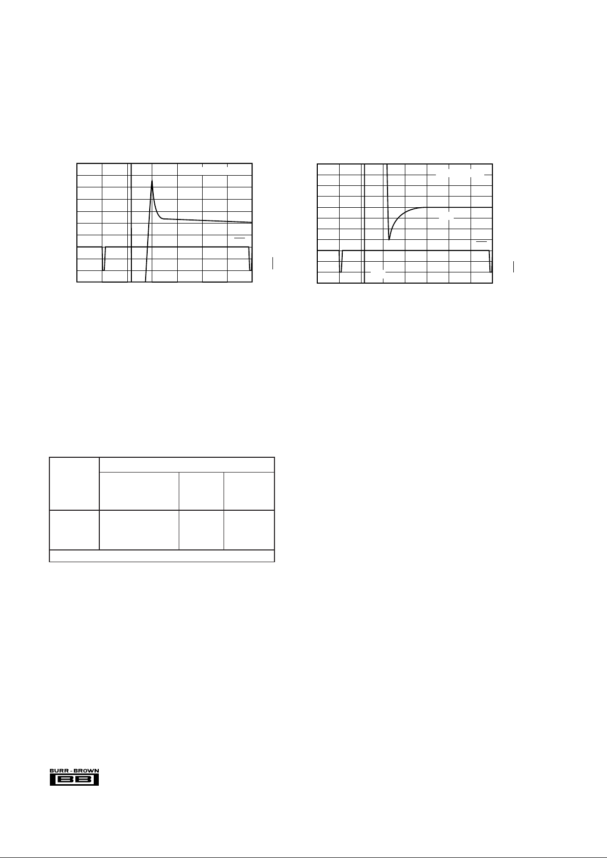
MAJOR CARRY GLITCH
Time (µs)
V
OUT
(mV)
250
200
150
100
50
0
–202468101214
+10
0
WR (V)
Data =
7FF
H
Data = 800
H
Data = 7FF
H
15
10
5
0
–5
–10
–15
0 5 10 15 20 25
Time (µs)
± FULL SCALE OUTPUT SWING
V (V)
OUT
WR
V
OUT
WR (V)
+5
0
0.5
0
–0.5
000
Input Code (Hexidecimal)
INTEGRAL LINEARITY ERROR
Linearity Error (LSB)
400 800 C00 FFF
1
0.5
0
–0.5
–1
–60 –20 20 60 100 140
Temperature (°C)
CHANGE OF GAIN AND OFFSET ERROR
vs TEMPERATURE
0.8
0.4
0
–0.4
–0.8
Gain Error
Bipolar
Offset
Unipolar
Offset
Bipolar/Unipolar Offset (%)
(For 10V FSR; Double for 20V FSR)
∆
Gain Error (%)∆
4
2
0
–2
–4
Input Current (µA)
–202468
Input Voltage (V)
DIGITAL INPUT CURRENT
vs INPUT VOLTAGE
LMSB, LDAC
Reset
LLSB, WR
Data
Frequency (Hz)
[Change in FSR]/[Change in Supply Voltage]
1k
10 100 1k 10k 100k 1M
POWER SUPPLY REJECTION vs
POWER SUPPLY RIPPLE FREQUENCY
(ppm of FSR/ %)
100
10
1
0.1
+V
CC
–V
CC
TYPICAL PERFORMANCE CURVES
At TA = +25°C, VCC = ±15V, unless otherwise noted.
®
6
DAC813
20
10
0
–10
–20
–40
Around +10V (mV)
–2
Time (µs)
SETTLING TIME, –10V TO +10V
+5
0
∆
WR (V)
02468101214
V
OUT
WR
V
OUT
1LSB = 4.88mV
20
10
0
–10
–20
Around –10V (mV)
–2
Time (µs)
SETTLING TIME, +10V TO –10V
+5
0
0 2 4 6 8 10 12
WR (V)
∆
1LSB = 4.88mV
V
OUT
WR
TYPICAL PERFORMANCE CURVES (CONT)
At TA = +25°C, VCC = ±15V, unless otherwise noted.
DISCUSSION OF
SPECIFICATIONS
INPUT CODES
The DAC813 accepts positive-true binary input codes.
DAC813 may be connected by the user for any one of the
following codes: USB (Unipolar Straight Binary), BOB
(Bipolar Offset Binary) or, using an external inverter on the
MSB line, BTC (Binary Two’s Complement). See Table I.
MONOTONICITY
A D/A converter is monotonic if the output either increases
or remains the same for increasing digital inputs. All grades
of DAC813 are monotonic over their specification temperature range.
DRIFT
Gain Drift is a measure of the change in the Full Scale Range
(FSR) output over the specification temperature range. Gain
Drift is expressed in parts per million per degree Celsius
(ppm/°C).
Unipolar Offset Drift is measured with a data input of
000
HEX
. The D/A is configured for unipolar output. Unipolar
Offset Drift is expressed in parts per million of Full Scale
Range per degree Celsius (ppm of FSR/°C).
Bipolar Zero Drift is measured with a data input of 800
HEX
.
The D/A is configured for bipolar output. Bipolar Zero Drift
is expressed in parts per million of Full Scale Range per
degree Celsius (ppm of FSR/°C).
SETTLING TIME
Settling Time is the total time (including slew time) for the
output to settle within an error band around its final value
after a change in input. Three settling times are specified to
±0.012% of Full Scale Range (FSR): two for maximum full
scale range changes of 20V and 10V, and one for a 1LSB
change. The 1LSB change is measured at the major carry
(7FF
HEX
to 800
HEX
and 800
HEX
to 7FF
HEX
), the input tran-
sition at which worst-case settling time occurs.
REFERENCE SUPPLY
DAC813 contains an on-chip +10V reference. This voltage
(pin 6) has a tolerance of ±50mV. V
REF OUT
must be con-
nected to V
REF IN
through a gain adjust resistor with a
nominal value of 500Ω. The connection can be made through
an optional 1kΩ trim resistor to provide adjustment to zero
DIGITAL ANALOG OUTPUT
INPUT
USB BOB BTC*
Unipolar Bipolar Binary
Straight Offset Two’s
MSB to LSB Binary Binary Complement
FFF
HEX
+ Full Scale + Full Scale Zero – 1LSB
800
HEX
+ 1/2 Full Scale Zero – Full Scale
7FF
HEX
+ 1/2 Full Scale – 1LSB Zero – 1LSB + Full Scale
000
HEX
Zero – Full Scale Zero
* Invert MSB of BOB code with external inverter to obtain BTC code.
TABLE I. Digital Input Codes.
LINEARITY ERROR
Linearity error as used in D/A converter specifications by
Burr-Brown is the deviation of the analog output from a
straight line drawn between the end points (inputs all “1s”
and all “0s”). The DAC813 linearity error is specified at
±1/4LSB (max) at +25°C K grades, and ±1/2LSB (max) for
J grades.
DIFFERENTIAL LINEARITY ERROR
Differential linearity error (DLE) is the deviation from a
1LSB output change from one adjacent state to the next. A
DLE specification of 1/2LSB means that the output step size
can range from 1/2LSB to 3/2LSB when the input changes
from one state to the next. Monotonicity requires that DLE
be less than 1LSB over the temperature range of interest.
7
®
DAC813
gain error. The reference output may be used to drive
external loads, sourcing at least 5mA. This current should be
constant, otherwise the gain of the converter will vary.
POWER SUPPLY SENSITIVITY
Power supply sensitivity is a measure of the effect of a
power supply change on the D/A converter output. It is
defined as a ppm of FSR output change per percent of
change in either +V
CC
or –VCC about the nominal voltages
expressed in ppm of FSR/%. The first performance curve on
page 5 shows typical power supply rejection versus power
supply ripple frequency.
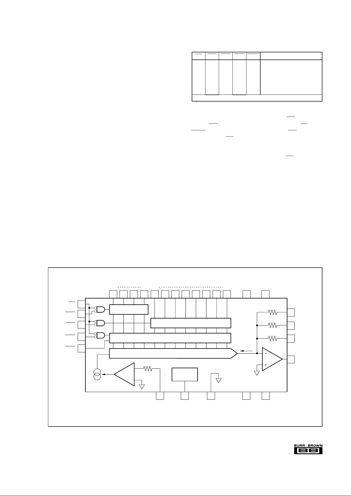
OPERATION
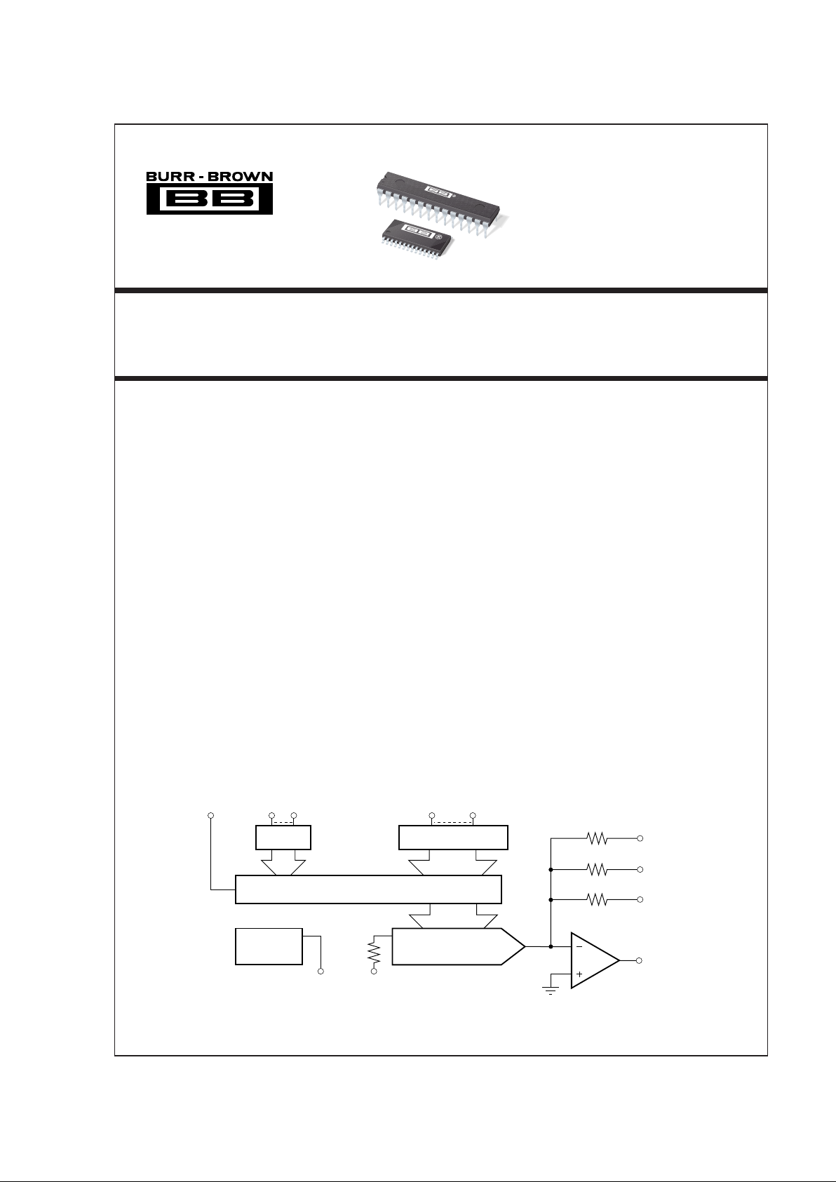
DAC813 is a complete single IC chip 12-bit D/A converter.
The chip contains a 12-bit D/A converter, voltage reference,
output amplifier, and microcomputer-compatible input logic
as shown in Figure 1.
INTERFACE LOGIC
Input latches hold data temporarily while a complete 12-bit
word is assembled before loading into the D/A latch. This
double-buffered organization prevents the generation of spurious analog output values. Each latch is independently
addressable.
All latches are level-triggered. Data present when the control signals are logic “0” will enter the latch. When any one
of the control signals returns to logic “1”, the data is latched.
A truth table for the control signals is presented in Table II.
FIGURE 1. DAC813 Block Diagram.
TABLE II. DAC813 Interface Logic Truth Table.
WR
LLSB LMSB LDAC RESET
OPERATION
1 X X X 1 No operation
XXXX0 D/A latch set to 800
HEX
01011 Enables 4 MSBs input latch
00111 Enables 8 LSBs input latch
01101
Loads D/A latch from input latches
00001Makes all latches transparent
“X” = Don’t Care
CAUTION: DAC813 was designed to use WR as the fast
strobe. WR has a much faster logic path than EN
X
(or
LDAC). Therefore, if one permanently wires WR to DCOM
and uses only ENX to strobe data into the latches, the
DATA HOLD time will be long, approximately 15ns to
30ns, and this time will vary considerably in this range
from unit to unit. DATA HOLD time using WR is 5ns max.
LOGIC INPUT COMPATIBILITY
The DAC813 digital inputs are TTL, 5V CMOS compatible over the operating range of +V
CC
. The input switching
threshold remains at the TTL threshold over the supply
range. An equivalent circuit of a digital input is shown in
Figure 2.
The logic input current over temperature is low enough to
permit driving the DAC813 directly from the outputs of 5V
CMOS devices.
Open DATA input lines will float to 7V or more. Although
this will not harm the DAC813, current spikes will occur in
the input lines when a logic 0 is asserted and, in addition,
LSB
D0
25kΩ
25k
Ω
24.9kΩ
BPO
20V
Range
V
OUT
12-Bit D/A Converter
12-Bit D/A Latch
4-Bit Latch
4
2
3
9
8-Bit Latch
28 27 26 25 24 23 22 21 20 19 18 17 161
MSB
D11 D8 D7 DCOM
0–800µA
7
49.5kΩ
6
+10V
Reference
5 8 10
+V
CC
–V
CC
ACOM
V
REF OUT
V
REF IN
11WR
14LMSB
15LLSB
12LDAC
13Reset
20V
Range
V
L
(1)
NOTE: (1) VL must be connected to +VCC.
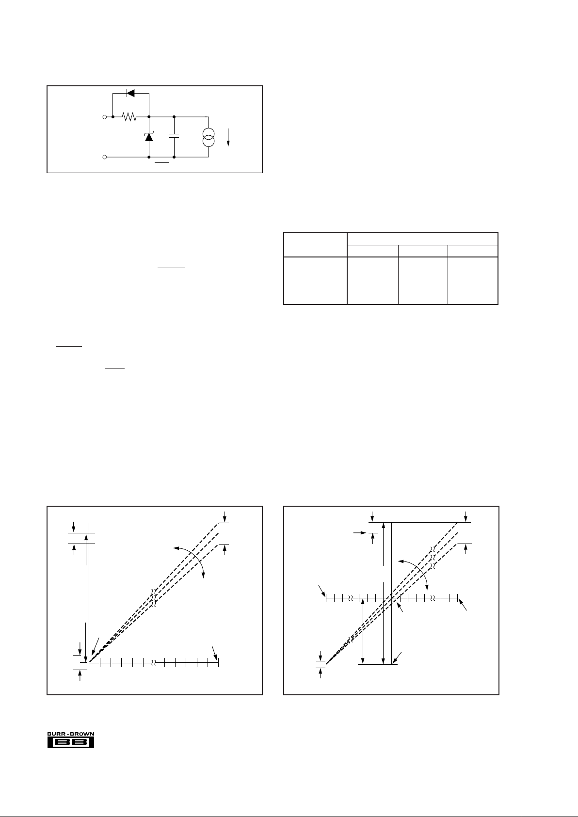
®
8
DAC813
See page 5
for I
I
FIGURE 2. Equivalent Input Circuit for Digital Inputs.
1kΩ
*
6.8V 5pF
Digital
Input
DCOM
* R = 500 for LLSB.Ω
I
I
the speed of the interface will be slower. A digital output
driving a DATA input line of the DAC813 must not drive,
or let the DATA input float, above +5.5V. Unused DATA
inputs should be connected to DCOM.
RESET FUNCTION
When asserted low (<0.8V), RESET (Pin 13) forces the
D/A latch to 800
HEX
regardless of any other input logic
condition. If the analog output is connected for bipolar
operation (either ±10V or ±5V), the output will be reset to
Bipolar Zero (0V). If the analog output is connected for
unipolar operation (0 to +10V), the output will be reset to
half-scale (+5V).
If RESET is not used, it should be connected to a voltage
greater than +2V but not greater than +5.5V. If this voltage
is not available Reset can be connected to +V
CC
through a
100kΩ to 1MΩ resistor to limit the input current.
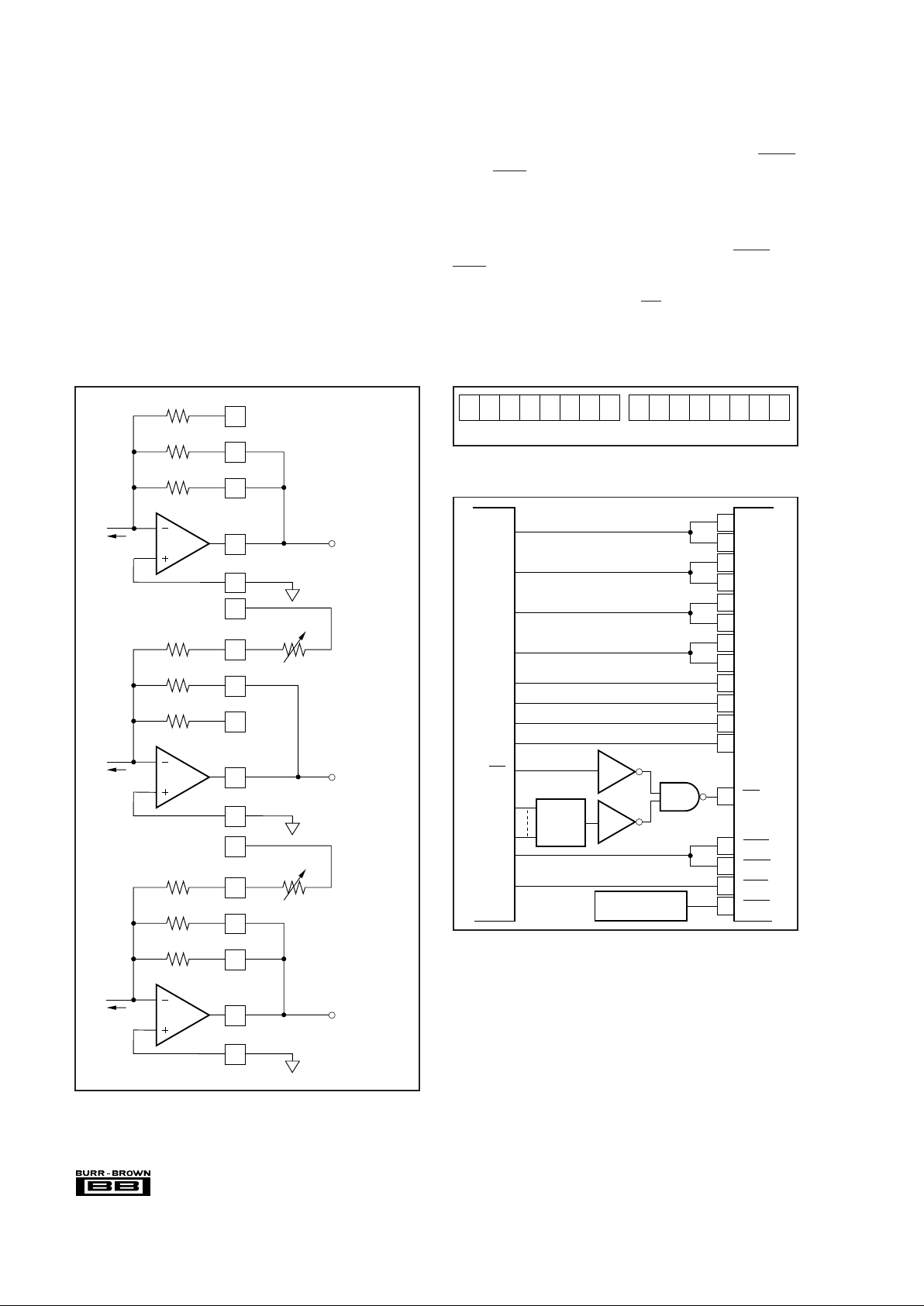
GAIN AND OFFSET ADJUSTMENTS
Figures 3 and 4 illustrate the relationship of offset and gain
adjustments to unipolar and bipolar D/A converter output.
OFFSET ADJUSTMENT
For unipolar (USB) configurations, apply the digital input
code that should produce zero voltage output and adjust the
offset potentiometer for zero output. For bipolar (BOB,
BTC) configurations, apply the digital input code that should
produce the maximum negative output voltage and adjust
the offset potentiometer for minus full scale voltage. Example: If the full scale range is connected for 20V, the
maximum negative output voltage is –10V. See Table III for
corresponding codes.
GAIN ADJUSTMENT
For either unipolar or bipolar configurations, apply the
digital input that should give the maximum positive voltage
output. Adjust the gain potentiometer for this positive full
scale voltage. See Table III for positive full scale voltages.
FIGURE 4. Relationship of Offset and Gain Adjustments
for a Bipolar D/A Converter.
FIGURE 3. Relationship of Offset and Gain Adjustments
for a Unipolar D/A Converter.
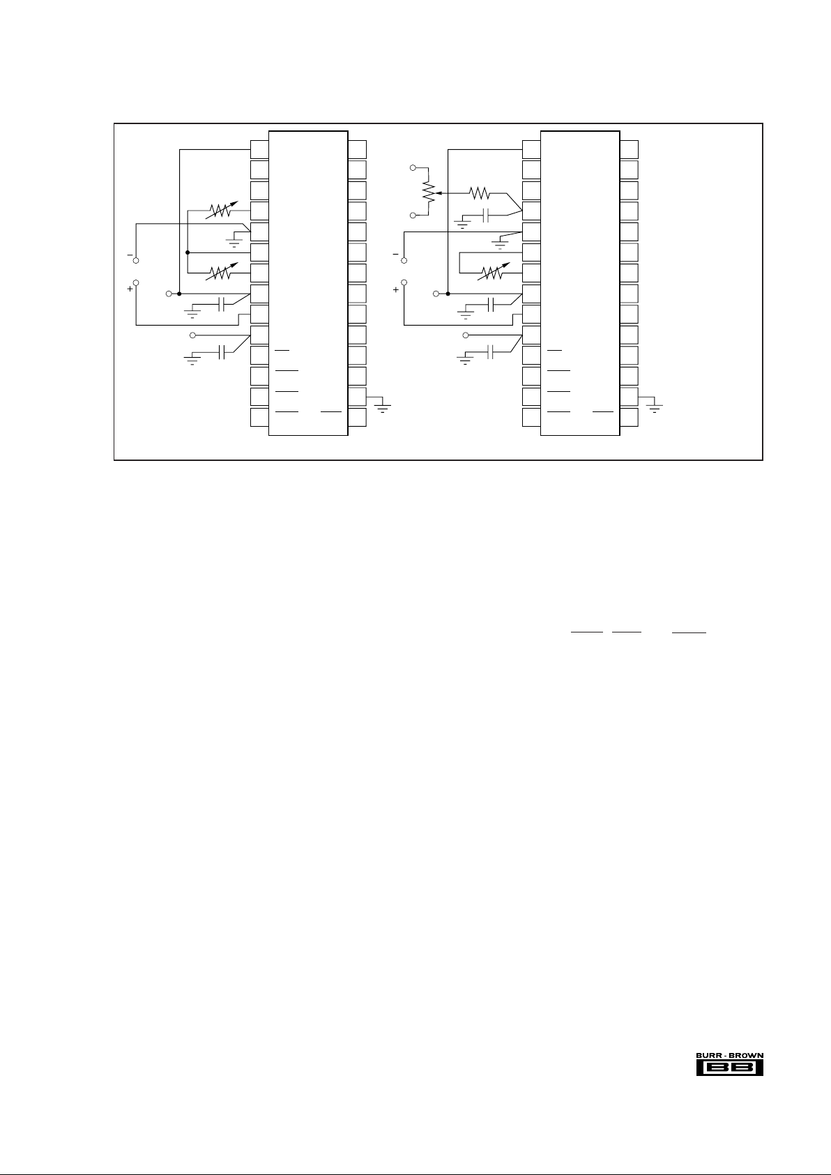
INSTALLATION
POWER SUPPLY CONNECTIONS
Note that the lid of the ceramic packaged DAC813 is
connected to –V
CC
. Take care to avoid accidental short
circuits in tightly spaced installations.
Power supply decoupling capacitors should be added as
shown in Figure 5. Optimum settling performance occurs
using a 1 to 10µF tantalum capacitor at –V
CC
and at least a
0.01µF ceramic capacitor at +V
CC
. Applications with less
critical settling time may be able to use 0.01µF at –V
CC
as
well. The 0.01µF capacitors should be located close to the
DAC813.
Pin 1 supplies internal logic and must be connected to +V
CC
.
+ Full Scale
All Bits
Logic 0
1LSB
Range of
Offset Adjust
Offset Adj.
Translates
the Line
Digital Input
All Bits
Logic 1
Analog Output
Full Scale
Range
Gain Adjust
Rotates the Line
– Full Scale
MSB on All
Others Off
Bipolar
Offset
Range of
Gain Adjust
≈ ±1%
≈ ±0.4%
+ Full Scale
All Bits
Logic 0
1LSB
Range of
Offset Adj.
Offset Adjust Translates the Line
Digital Input
All Bits
Logic 1
Range of
Gain Adjust
Analog Output
Gain Adjust
Rotates the Line
Full Scale Range
≈ ±0.4%
≈ ±1%
DIGITAL INPUT ANALOG OUTPUT
MSB to LSB 0 to +10V
±5V ±10V
FFF
HEX
+9.9976V +4.9976V +9.9951V
800
HEX
+5.0000V 0.0000V 0.0000V
7FF
HEX
+4.9976V –0.0024V –0.0049V
000
HEX
0.0000V –5.0000V –10.0000V
1LSB 2.44mV 2.44mV 4.88mV
TABLE III. Digital Input/Analog Output.
9
®
DAC813
FIGURE 5. Power Supply, Gain, and Offset Connections.
200Ω
1
2
3
4
5
6
7
8
9
10
11
12
13
14
28
27
26
25
24
23
22
21
20
19
18
17
16
15
1kΩ
V
OUT
3MΩ
1
2
3
4
5
6
7
8
9
10
11
12
13
14
28
27
26
25
24
23
22
21
20
19
18
17
16
15
1kΩ
V
OUT
–V
CC
10k to
100k
BIPOLAR UNIPOLAR
(2)
(1) 10µF tantalum for
optimum settling
performance.
(2) Unipolar offset is
not necessary in most
applications and can
lead to noise pickup.
(3) Note that for the
ceramic package
the lid is connected
to –V
Ω
Ω
++
0.01µF
0.01µF
+V
CC
CC
.
L
REF OUT
REF IN
CC
OUT
CC
V
20V Range
20V Range
BPO
ACOM
V
V
+V
V
–V
WR
LDAC
Reset
LMSB
D11
D10
D9
D8
D7
D6
D5
D4
D3
D2
D1
D0
DCOM
LLSB
(1)
0.01µF
(1)
0.01µF
0.01µF
L
REF OUT
REF IN
CC
OUT
CC
V
20V Range
20V Range
BPO
ACOM
V
V
+V
V
–V
WR
LDAC
Reset
LMSB
D11
D10
D9
D8
D7
D6
D5
D4
D3
D2
D1
D0
DCOM
LLSB
+V
CC
+V
CC
–V
CC
(3)
–V
CC
(3)
DAC813 features separate digital and analog power supply
returns to permit optimum connections for low noise and
high speed performance. It is recommended that both Analog Common (ACOM, Pin 5) and Digital Common (DCOM,
Pin 16) be connected directly to a ground plane under the
package. If a ground plane is not used, connect the ACOM
and DCOM pins together close to the package. Since the
reference point for V
OUT
and V
REF OUT
is the ACOM pin, it
is also important to connect the load directly to the ACOM
pin. Refer to Figure 5.
The change in current in the Analog Common pin (ACOM,
Pin 5) due to an input data word change from 000
HEX
to
FFF
HEX
is only 800µA.
OUTPUT RANGE CONNECTIONS
Internal scaling resistors provided in the DAC813 may be
connected to produce bipolar output voltage ranges of ±10V
and ±5V or unipolar output voltage range of 0 to +10V.
Refer to Figure 6.
The internal feedback resistors (25kΩ) and the bipolar offset
resistor (24.9kΩ) are trimmed to an absolute tolerance of
less than ±2%. Therefore, one can change the range by
adding a series resistor in various feedback circuit configurations. For example, a 600Ω resistor in series with the 20V
range terminal can be used to obtain a 20.48V (±10.24V)
range (5mV LSB). A 7.98kΩ resistor in series with the 10V
range connection (20V ranges in parallel) gives a 16.384V
(±8.192V) bipolar range (4mV LSB). Gain drift will be
affected by the mismatch of the temperature coefficient of
the external resistor with the internal D/A resistors.
APPLICATIONS
MICROCOMPUTER BUS INTERFACING
The DAC813 interface logic allows easy interface to microcomputer bus structures. The control signal is derived from
external device select logic and the I/O Write or Memory
Write (depending upon the system design) signals from the
microcomputer.
The latch enable lines LMSB, LLSB, and LDAC determine
which of the latches are selected. It is permissible to enable
two or more latches simultaneously, as shown in some of the
following examples.
The double-buffered latch permits data to be loaded into the
input latches of several DAC813s and later strobed into the
D/A latch of all D/As, simultaneously updating all analog
outputs. All the interface schemes shown below use a base
address decoder. If blocks of memory are used, the base
address decoder can be simplified or eliminated altogether.
8-BIT INTERFACE
The control logic of DAC813 permits interfacing to rightjustified data formats, illustrated in Figure 7. When a 12-bit
D/A converter is loaded from an 8-bit bus, two bytes of data
are required. Figure 8 illustrates an addressing scheme for
right-justified data. The base address is decoded from the
high-order address bits. A0 and A1 address the appropriate
latches. Note that adjacent addresses are used. X10
HEX
loads
the 8 LSBs and X01
HEX
loads the 4 MSBs and simultaneously transfers input latch data to the D/A latch. Addresses
X00
HEX
and X11
HEX
are not used.
®
10
DAC813
INTERFACING MULTIPLE
DAC813s IN 8-BIT SYSTEMS
Many applications, such as automatic test systems, require
that the outputs of several D/A converters be updated simultaneously. The interface shown in Figure 9 uses a 74LSB138
decoder to decode a set of eight adjacent addresses to load
the input latches of four DAC813s. The example uses a
right-justified data format.
A ninth address using A3 causes all DAC813s to be updated
simultaneously. If a certain DAC813 is always loaded last
(for instance, D/A #4), A3 is not needed, saving 8 address
spaces for other uses. Incorporate A3 into the base address
decoder, remove the inverter, connect the common LDAC
line to LLSB of D/A #4, and connect D1 of the 74LS138 to
+5V.
12- AND 16-BIT MICROCOMPUTER INTERFACE
For this application the input latch enable lines, LMSB and
LLSB, are tied low, causing the latches to be transparent.
The D/A latch, and therefore DAC813, is selected by the
address decoder and strobed by WR.
Be sure and read the CAUTION statement in the LOGIC
INPUT COMPATIBILITY section.
FIGURE 6. Output Amplifier Voltage Range Scaling Circuit.
25kΩ
25kΩ
24.9kΩ
9
3
2
4
BPO
20V
20V
V
OUT
±5V
6
200 pot or
100 fixedΩΩ
±5V
RANGE
25kΩ
25kΩ
24.9kΩ
9
3
2
4
BPO
20V
20V
V
OUT
±10V
V
REF OUT
6
200 pot or
100 fixedΩΩ
±10V
RANGE
25kΩ
25kΩ
24.9kΩ
9
3
2
4
BPO
20V
20V
V
OUT
0 to +10V
0 TO +10V
RANGE
NC
NC
I
DAC
I
DAC
I
DAC
5
5
V
REF OUT
5
ACOM
ACOM
ACOM
FIGURE 8. Right-Justified Data Bus Interface.
D0
D8
D1
D9
D2
D10
D3
D11
D4
D5
D6
D7
17
25
18
26
19
27
20
28
21
22
23
24
DB0
DB1
DB2
DB3
Reset Circuitry
DB4
DB5
DB6
DB7
WR
A
A
1
0
Microcomputer
DAC813
Base
Address
Decoder
A
A
15
2
11
12
14
15
13
WR
LDAC
LMSB
LLSB
Reset
X X X X D11D10 D9 D8 D7 D6 D5 D4 D3 D2 D1 D0
Right-Justified
FIGURE 7. 12-Bit Data Format for 8-Bit Systems.
11
®
DAC813
FIGURE 9. Interfacing Multiple DAC813s to an 8-Bit Bus.
Base
Address
Decoder
WR
A
A
15
4
A
A
A
2
1
0
Microcomputer
A
3
74LS138
C
B
A
G
G
G
2A
2B
1
DAC813
(1)
DAC813
(2)
WR
LDAC
LLSB
LMSB
DAC813
(4)
Y0
Y1
Y2
Y3
Y4
Y5
Y6
Y7
15
14
13
12
11
10
9
7
3
2
1
4
6
5
CS
WR
LDAC
LLSB
LMSB
WR
LDAC
LLSB
LMSB
ADDRESS BUS
A3 A2 A1 A0 OPERATION
0 0 0 0 Load 8 LSB – D/A #1
0 0 0 1 Load 4 MSB – D/A #1
0 0 1 0 Load 8 LSB – D/A #2
0 0 1 1 Load 4 MSB – D/A #2
0 1 0 0 Load 8 LSB – D/A #3
0 1 0 1 Load 4 MSB – D/A #3
0 1 1 0 Load 8 LSB – D/A #4
0 1 1 1 Load 4 MSB – D/A #4
1 X X X Load D/A Latch—All D/A
 Loading...