

Datasheet DAC7613EB-1K, DAC7613EB, DAC7613E-1K, DAC7613E Datasheet (Burr Brown Corporation)
Page 1
1
®
DAC7613
12-Bit, Voltage Output
DIGITAL-TO-ANALOG CONVERTER
®
DAC7613
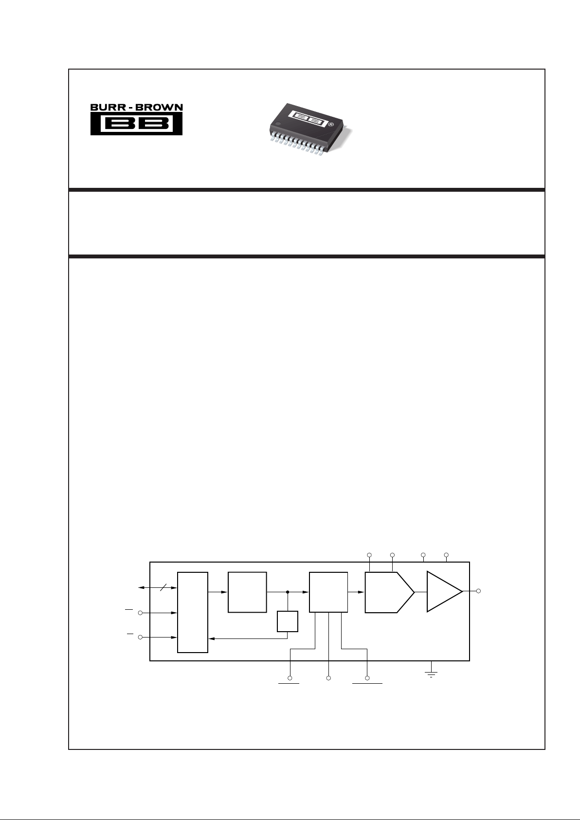
DESCRIPTION
The DAC7613 is a 12-bit, voltage output digital-toanalog converter with guaranteed 12-bit monotonic
performance over the specified temperature range.
The DAC7613 accepts a 12-bit parallel input data, has
double-buffered DAC input logic and provides a
readback mode of the internal input register. An asynchronous reset clears all registers to a mid-scale code
of 800H or to a zero-scale of 000H. The DAC7613 can
operate from a single +5V supply or from +5V and
–5V supplies.
Low power and small size makes the DAC7613 ideal
for data acquisition systems and closed-loop servocontrol. The DAC7613 is available in a plastic
SSOP-24 package, and offers guaranteed specifications over the –40°C to +85°C temperature range.
FEATURES
● LOW POWER: 1.8mW
● UNIPOLAR OR BIPOLAR OPERATION
● SETTLING TIME: 10µs to 0.012%
● 12-BIT LINEARITY AND MONOTONICITY:
–40°C to +85°C
● DATA READBACK
● DOUBLE-BUFFERED DATA INPUTS
● 24-LEAD SSOP PACKAGE
APPLICATIONS
● PROCESS CONTROL
● CLOSED-LOOP SERVO-CONTROL
● MOTOR CONTROL
● DATA ACQUISITION SYSTEMS
© 1998 Burr-Brown Corporation PDS-1500B Printed in U.S.A. January, 2000
International Airport Industrial Park • Mailing Address: PO Box 11400, Tucson, AZ 85734 • Street Address: 6730 S. Tucson Blvd., Tucson, AZ 85706 • Tel: (520) 746-1111
Twx: 910-952-1111 • Internet: http://www.burr-brown.com/ • Cable: BBRCORP • Telex: 066-6491 • FAX: (520) 889-1510 • Immediate Product Info: (800) 548-6132
TS
DAC
Register
DAC
DAC7613
Input
Register
I/O
Buffer
Data I/O
CS
12
R/W
V
REFL
V
OUT
RESET RESETSEL LOADDAC GND
V
REFH
V
DDVSS
DAC7613
For most current data sheet and other product
information, visit www.burr-brown.com
Page 2
2
®
DAC7613
SPECIFICATION
At TA = –40°C to +85°C, VDD = +5V, VSS = –5V, V
REFH
= +2.5V, and V
REFL
= –2.5V, unless otherwise noted.
The information provided herein is believed to be reliable; however, BURR-BROWN assumes no responsibility for inaccuracies or omissions. BURR-BROWN assumes
no responsibility for the use of this information, and all use of such information shall be entirely at the user’s own risk. Prices and specifications are subject to change
without notice. No patent rights or licenses to any of the circuits described herein are implied or granted to any third party. BURR-BROWN does not authorize or warrant
any BURR-BROWN product for use in life support devices and/or systems.
DAC7613E DAC7613EB
NOTES: (1) If VSS = 0V, specification applies at code 00AH and above. (2) LSB means Least Significant Bit, when V
REFH
equals +2.5V and V
REFL
equals –2.5V,
then one LSB equals 1.22mV. (3) Ideal output voltage, does not take into account zero or full-scale error. (4) If V
SS
= –5V, full-scale 5V step. If VSS = 0V, full-scale
positive 2.5V step and negative step from code FFF
H
to 00AH.
PARAMETER CONDITIONS MIN TYP MAX MIN TYP MAX UNITS
ACCURACY
Linearity Error
(1)
VSS = 0V or –5V ±2 ±1 LSB
(2)
Differential Linearity Error VSS = 0V or –5V ±1 ±1 LSB
Monotonicity T
MIN
to T
MAX
12 ✻ Bits
Zero-Scale Error Code = 000
H
±4 ✻ LSB
Zero-Scale Drift 25 ✻✻ppm/°C
Full-Scale Error Code = FFF
H
±4 ✻ LS
Zero-Scale Error Code = 00A
H
, VSS = 0V ±8 ✻ LSB
Zero-Scale Drift VSS = 0V 5 10 ✻✻ppm/°C
Full-Scale Error Code = FFFH, VSS = 0V ±8 ✻ LSB
Power Supply Rejection 30 ✻ ppm/V
ANALOG OUTPUT
Voltage Output
(3)
V
REFL
= 0V, VSS = 0V 0 V
REFH
✻✻V
VSS = –5V V
REFL
V
REFH
✻✻V
Output Current –1.25 +1.25 ✻✻mA
Load Capacitance No Oscillation 100 ✻ pF
Short-Circuit Current +5, –15 ✻ mA
Short-Circuit Duration
Indefinite
✻
REFERENCE INPUT
V
REFH
Input Range VSS = 0V or –5V
V
REFL
+ 1.25
+2.5 ✻✻V
V
REFL
Input Range VSS = 0V 0
V
REFH
– 1.25
✻✻V
V
REFL
Input Range VSS = –5V –2.5
V
REFH
– 1.25
✻✻V
DYNAMIC PERFORMANCE
Settling Time
(4)
To ±0.012% 5 10 ✻✻ µs
Output Noise Voltage 0Hz to 1MHz 40 ✻ nV/√Hz
DIGITAL INPUT/OUTPUT
Logic Family CMOS ✻
Logic Levels
V
IH
IIH ≤ ±10µA 0.7 V
DD
VDD + 0.3 ✻✻V
V
IL
IIL ≤ ±10µA –0.3 0.3 V
DD
✻✻V
V
OH
IOH = –0.8mA 3.6 V
DD
✻✻V
V
OL
IOL = 1.6mA 0.0 0.4 ✻✻V
Data Format Straight Binary ✻
POWER SUPPLY REQUIREMENTS
V
DD
4.75 5.25 ✻✻V
V
SS
If VSS ≠ 0V –5.25 –4.75 ✻✻V
I
DD
0.35 0.5 ✻✻ mA
I
SS
–0.65 –0.45 ✻✻ mA
Power Dissipation V
SS
= –5V 4 5.75 ✻✻ mW
V
SS
= 0V 1.8 2.5 ✻✻ mW
TEMPERATURE RANGE
Specified Performance –40 +85 ✻✻°C
Page 3
3
®
DAC7613
ABSOLUTE MAXIMUM RATINGS
(1)
V
DD
to VSS............................................................................. –0.3V to 11V
V
DD
to GND .......................................................................... –0.3V to 5.5V
V
REFL
to VSS..............................................................–0.3V to (V
DD
– VSS)
V
DD
to V
REFH
............................................................. –0.3V to (V
DD
– VSS)
V
REFH
to V
REFL
..........................................................–0.3V to (V
DD
– VSS)
Digital Input Voltage to GND ................................... –0.3V to V
DD
+ 0.3V
Digital Output Voltage to GND ................................. –0.3V to V
DD
+ 0.3V
Maximum Junction Temperature................................................... +150°C
Operating Temperature Range ........................................ –40°C to +85°C
Storage Temperature Range ......................................... –65°C to +150°C
Lead Temperature (soldering, 10s) ............................................... +300°C
NOTE: (1) Stresses above those listed under “Absolute Maximum Ratings”
may cause permanent damage to the device. Exposure to absolute maximum
conditions for extended periods may affect device reliability.
ELECTROSTATIC
DISCHARGE SENSITIVITY
This integrated circuit can be damaged by ESD. Burr-Brown
recommends that all integrated circuits be handled with
appropriate precautions. Failure to observe proper handling
and installation procedures can cause damage.
ESD damage can range from subtle performance degradation
to complete device failure. Precision integrated circuits may
be more susceptible to damage because very small parametric
changes could cause the device not to meet its published
specifications.
PACKAGE/ORDERING INFORMATION
MAXIMUM MAXIMUM
LINEARITY DIFFERENTIAL PACKAGE SPECIFICATION
ERROR LINEARITY ERROR DRAWING TEMPERATURE ORDERING TRANSPORT
PRODUCT (LSB) (LSB) PACKAGE NUMBER RANGE NUMBER
(1)
MEDIA
DAC7613E ±2 ±1 SSOP-24 338 –40°C to +85°C DAC7613E Rails
""""""DAC7613E/1K Tape and Reel
DAC7613EB ±1 ±1 SSOP-24 338 –40°C to +85°C DAC7613EB Rails
""""""DAC7613EB/1K Tape and Reel
NOTE: (1) Models with a slash (/) are available only in Tape and Reel in the quantities indicated (e.g., /1K indicates 1000 devices per reel). Ordering 1000 pieces
of “DAC7613E/1K” will get a single 1000-piece Tape and Reel.
Page 4

4
®
DAC7613
Top View SSOP
PIN DESCRIPTIONS
PIN CONFIGURATION
PIN LABEL DESCRIPTION
1 DB11 Data Bit 11, MSB
2 DB10 Data Bit 10
3 DB9 Data Bit 9
4 DB8 Data Bit 8
5 DB7 Data Bit 7
6 DB6 Data Bit 6
7 DB5 Data Bit 5
8 DB4 Data Bit 4
9 DB3 Data Bit 3
10 DB2 Data Bit 2
11 DB1 Data Bit 1
12 DB0 Data Bit 0, LSB
13 V
REFL
Reference Input Voltage Low. Sets minimum out-
put voltage for the DAC.
14 NIC Not Internally Connected
15 V
REFH
Reference Input Voltage High. Sets maximum
output voltage for the DAC.
16 V
SS
Negative Analog Supply Voltage, 0V or –5V
nominal.
17 GND Ground
18 V
DD
Positive Power Supply
19 V
OUT
DAC Voltage Output
20 LOADDAC The selected DAC register becomes transparent
when LOADDAC is LOW. It is in the latched state
when LOADDAC is HIGH.
21 RESET Asynchronous Reset Input. Sets the DAC register
to either zero-scale (000
H
) or mid-scale (800H)
when LOW. RESETSEL determines which code is
active.
22 RESETSEL When LOW, a LOW on RESET will cause the DAC
register to be set to code 000
H
. When RESETSEL
is HIGH, a LOW on RESET will set the registers to
code 800
H
.
23 CS Chip Select. Active LOW.
24 R/W Enabled by CS. Controls data read and write from
the input register.
1
2
3
4
5
6
7
8
9
10
11
12
24
23
22
21
20
19
18
17
16
15
14
13
DB11 (MSB)
DB10
DB9
DB8
DB7
DB6
DB5
DB4
DB3
DB2
DB1
DB0 (LSB)
R/W
CS
RESETSEL
RESET
LOADDAC
V
OUT
V
DD
GND
V
SS
V
REFH
NIC
V
REFL
DAC7613E
Page 5

5
®
DAC7613
TYPICAL PERFORMANCE CURVES: VSS = 0V
At TA = +25°C, VDD = +5V, V
REFH
= +2.5V, and V
REFL
= 0V, representative unit, unless otherwise specified.
LINEARITY ERROR and
DIFFERENTIAL LINEARITY ERROR vs CODE
200
H
000
H
Digital Input Code
DLE (LSB) LE (LSB)
0.50
0.00
–0.25
–0.50
0.50
0.25
0.00
–0.50
–0.25
0.25
400H600H800HA00HC00HE00HFFF
H
LINEARITY ERROR vs CODE
(–40°C and +85°C)
000
H
Digital Input Code
LE (LSB) LE (LSB)
0.50
0.00
–0.25
–0.50
0.50
0.25
0.00
–0.50
–0.25
0.25
200H400H600H800HA00HC00HE00HFFF
H
+85°C
–40°C
DIFFERENTIAL LINEARITY ERROR vs CODE
(–40°C and +85°C)
000
H
Digital Input Code
DLE (LSB) DLE (LSB)
0.50
0.00
–0.25
–0.50
0.50
0.25
0.00
–0.50
–0.25
0.25
200H400H600H800HA00HC00HE00HFFF
H
+85°C
–40°C
ZERO-SCALE ERROR vs TEMPERATURE
(Code 010
H
)
20–40 100–20 0 40
Temperature (°C)
Zero-Scale Error (LSB)
–2
6
4
3
0
–1
5
1
2
60 80
FULL-SCALE ERROR vs TEMPERATURE
(Code FFF
H
)
20–40 100–20 0 40
Temperature (°C)
Full-Scale Error (LSB)
–2
6
4
3
0
–1
5
1
2
60 80
Page 6

6
®
DAC7613
TYPICAL PERFORMANCE CURVES: VSS = – 5V
At TA = +25°C, VDD = +5V, V
REFH
= +2.5V, and V
REFL
= 0V, representative unit, unless otherwise specified.
LINEARITY ERROR vs CODE
000
H
Digital Input Code
LE (LSB) LE (LSB)
0.50
0.00
–0.25
–0.50
0.50
0.25
0.00
–0.50
–0.25
0.25
200H400H600H800HA00HC00HE00HFFF
H
DIFFERENTIAL LINEARITY ERROR vs CODE
000
H
Digital Input Code
DLE (LSB) DLE (LSB)
0.50
0.00
–0.25
–0.50
0.50
0.25
0.00
–0.50
–0.25
0.25
200H400H600H800HA00HC00HE00HFFF
H
ZERO-SCALE ERROR vs TEMPERATURE
(Code 000
H
)
20–40 100–20 0 40
Temperature (°C)
Zero-Scale Error (LSB)
–1.0
3.0
2.0
1.5
0.0
–0.5
2.5
0.5
1.0
60 80
FULL-SCALE ERROR vs TEMPERATURE
(Code FFF
H
)
20–40 100–20 0 40
Temperature (°C)
Full-Scale Error (LSB)
–1.0
3.0
2.0
1.5
0.0
–0.5
2.5
0.5
1.0
60 80
LINEARITY ERROR and
DIFFERENTIAL LINEARITY ERROR vs CODE
000
H
Digital Input Code
DLE (LSB) LE (LSB)
0.50
0.00
–0.25
–0.50
0.50
0.25
0.00
–0.50
–0.25
0.25
200H400H600H800HA00HC00HE00HFFF
H
Page 7

7
®
DAC7613
THEORY OF OPERATION
The DAC7613 is a 12-bit, voltage output Digital-to-Analog
Converter (DAC). The architecture is a classic R-2R ladder
configuration followed by an operational amplifier that serves
as a buffer. The minimum voltage output (“zero-scale”) and
maximum voltage output (“full-scale”) are set by the external voltage references (V
REFL
and V
REFH
, respectively). The
digital input is a 12-bit parallel word and the DAC input
register offers a readback capability. The converter can be
powered from a single +5V supply or a dual ±5V supply.
The device offers a reset function which immediately sets
the DAC output voltage and DAC register to mid-scale
(code 800H) or to zero-scale (code 000H), depending on the
status of the reset selection. See Figures 1 and 2 for the basic
operation of the DAC7613.
FIGURE 1. Basic Single-Supply Operation of the DAC7613.
FIGURE 2. Basic Dual-Supply Operation of the DAC7613.
1
2
3
4
5
6
7
8
9
10
11
12
24
23
22
21
20
19
18
17
16
15
14
13
DB11
DB10
DB9
DB8
DB7
DB6
DB5
DB4
DB3
DB2
DB1
DB0
R/W
CS
RESETSEL
RESET
LOADDAC
V
OUT
V
DD
GND
V
SS
V
REFH
NIC
V
REFL
Read/Write
Chip Select
Reset Select
Reset DAC
Load DAC Register
0V to +2.5V
DAC7613E
+5V
Data Bus
+2.5V
0.1µF1µF
0.1µF
+
1
2
3
4
5
6
7
8
9
10
11
12
24
23
22
21
20
19
18
17
16
15
14
13
DB11
DB10
DB9
DB8
DB7
DB6
DB5
DB4
DB3
DB2
DB1
DB0
R/W
CS
RESETSEL
RESET
LOADDAC
V
OUT
V
DD
GND
V
SS
V
REFH
NIC
V
REFL
Read/Write
Chip Select
Reset Select
Reset DAC
Load DAC Register
–2.5V to +2.5V
DAC7613E
+5V
Data Bus
–5V
0.1µF1µF
1µF
0.1µF
+2.5V
0.1µF
–2.5V
0.1µF
+
+
Page 8

8
®
DAC7613
ANALOG OUTPUTS
When VSS = –5V (dual supply operation), the output amplifier can swing to within 2.25V of the supply rails, guaranteed over the –40°C to +85°C temperature range. With
VSS = 0V (single-supply operation), the output can swing to
ground. Note that the settling time of the output op amp will
be longer with voltages very near ground. Additionally, care
must be taken when measuring the zero-scale error when
VSS = 0V. Since the output voltage cannot swing below
ground, the output voltage may not change for the first few
digital input codes (000H, 001H, 002H, etc.) if the output
amplifier has a negative offset.
The behavior of the output amplifier can be critical in some
applications. Under short-circuit conditions (DAC output
shorted to ground), the output amplifier can sink a great deal
more current than it can source. See the Specifications table
for more details concerning short-circuit current.
REFERENCE INPUTS
The reference inputs, V
REFL
and V
REFH
, can be any voltage
between V
SS
+ 2.25V and V
DD
– 2.25V provided that V
REFH
is at least 1.25V greater than V
REFL
. The minimum output of
each DAC is equal to V
REFL
plus a small offset voltage
(essentially, the offset of the output op amp). The maximum
output is equal to V
REFH
plus a similar offset voltage. Note
that VSS (the negative power supply) must either be
connected to ground or must be in the range of –4.75V to
–5.25V. The voltage on VSS sets several bias points within
the converter. If VSS is not in one of these two configurations, the bias values may be in error and proper operation
of the device is not guaranteed.
The current into the V
REFH
input depends on the DAC output
voltages and can vary from a few microamps to approximately 0.1 milliamp. The V
REFH
source will not be required
to sink current, only source it. Bypassing the reference
voltage or voltages with at least a 0.1µF capacitor placed as
close to the DAC7613 package is strongly recommended.
DIGITAL INTERFACE
Table I shows the basic control logic for the DAC7613. Note
that the internal register is level triggered and not edge
triggered. When the appropriate signal is LOW, the register
becomes transparent. When this signal is returned HIGH, the
digital word currently in the register is latched. The first
register (the input register) is triggered via the R/W, and CS
inputs. The second register (the DAC register) is transparent
when LOADDAC input is pulled LOW.
The double-buffered architecture is mainly designed so that
the DAC input register can be written at any time and then
the DAC voltage updated by pulling LOADDAC LOW.
INPUT DAC
R/W CS RST LOADDAC REGISTER REGISTER MODE
L L H L Write Write Write
L L H H Write Hold Write Input
H L H H Read Hold Read Input
X H H L Hold Update Update
X H H H Hold Hold Hold
X H L X Hold Reset Reset
X = Don’t Care.
TABLE I. DAC7613 Control Logic Truth Table.
Page 9

9
®
DAC7613
V
OUT
= V
REFL
+
V
REFH–VREFL
()
•N
4096
DIGITAL TIMING
Figure 3 and Table II provide detailed timing for the digital
interface of the DAC7613.
DIGITAL INPUT CODING
The DAC7613 input data is in Straight Binary format. The
output voltage is given by the following equation:
(1)
where N is the digital input code. This equation does not
include the effects of offset (zero-scale) or gain (full-scale)
errors.
FIGURE 3. Digital Input and Output Timing.
t
RCS
CS
t
RDS
t
RDH
t
CSD
t
DZ
R/W
Data Out
Data Valid
t
WCS
CS
t
WS
t
WH
R/W
t
RESET
t
LWD
LOADDAC
t
DS
t
DH
Data In
RESET
Data Output Timing
Digital Input Timing
SYMBOL
DESCRIPTION MIN TYP MAX UNITS
t
RCS
CS LOW for Read 200 ns
t
RDS
R/W HIGH to CS LOW 10 ns
t
RDH
R/W HIGH after CS HIGH 0 ns
t
DZ
CS HIGH to Data Bus in 100 ns
High Impedance
t
CSD
CS LOW to Data Bus Valid 100 160 ns
t
WCS
CS LOW for Write 50 ns
t
WS
R/W LOW to CS LOW 0 ns
t
WH
R/W LOW after CS HIGH 5 ns
t
DS
Data Valid to CS LOW 0 ns
t
DH
Data Valid after CS HIGH 5 ns
t
LWD
LOADDAC LOW 50 ns
t
RESET
RESET LOW 50 ns
TABLE II. Timing Specifications (TA = –40°C to +85°C).
 Loading...