

Datasheet DAC7611UB-2K5, DAC7611UB, DAC7611U-2K5, DAC7611U, DAC7611PB Datasheet (Burr Brown Corporation)
...Page 1
®
1
DAC7611
®
International Airport Industrial Park • Mailing Address: PO Box 11400, Tucson, AZ 85734 • Street Address: 6730 S. Tucson Blvd., Tucson, AZ 85706 • Tel: (520) 746-1111 • Twx: 910-952-1111
Internet: http://www.burr-brown.com/ • FAXLine: (800) 548-6133 (US/Canada Only) • Cable: BBRCORP • Telex: 066-6491 • FAX: (520) 889-1510 • Immediate Product Info: (800) 548-6132
DAC7611
12-Bit Serial Input
DIGITAL-TO-ANALOG CONVERTER
DESCRIPTION
The DAC7611 is a 12-bit digital-to-analog converter
(DAC) with guaranteed 12-bit monotonicity performance over the industrial temperature range. It requires a single +5V supply and contains an input shift
register, latch, 2.435V reference, DAC, and high speed
rail-to-rail output amplifier. For a full-scale step, the
output will settle to 1 LSB within 7µs. The device
consumes 2.5mW (0.5mA at 5V).
The synchronous serial interface is compatible with a
wide variety of DSPs and microcontrollers. Clock
(CLK), serial data in (SDI), and load strobe (LD)
comprise the serial interface. In addition, two control
pins provide a chip select (CS) function and an asynchronous clear (CLR) input. The CLR input can be
used to ensure that the DAC7611 output is 0V on
power-up or as required by the application.
The DAC7611 is available in an 8-lead SOIC or 8-pin
plastic DIP package and is fully specified over the
industrial temperature range of –40°C to +85°C.
DAC7611
DAC7611
© 1997 Burr-Brown Corporation PDS-1402A Printed in U.S.A. April, 1998
FEATURES
● LOW POWER: 2.5mW
● FAST SETTLING: 7
µs to 1 LSB
● 1mV LSB WITH 4.095V FULL-SCALE
RANGE
● COMPLETE WITH REFERENCE
● 12-BIT LINEARITY AND MONOTONICITY
OVER INDUSTRIAL TEMP RANGE
● ASYNCHRONOUS RESET TO 0V
● 3-WIRE INTERFACE: Up to 20MHz Clock
● ALTERNATE SOURCE TO DAC8512
12-Bit DAC
Ref
DAC Register
Serial Shift Register
12
12
CLR
LD
CS
CLK
SDI
V
DD
GND
V
OUT
DAC7611
APPLICATIONS
● PROCESS CONTROL
● DATA ACQUISITION SYSTEMS
● CLOSED-LOOP SERVO-CONTROL
● PC PERIPHERALS
● PORTABLE INSTRUMENTATION
Page 2
®
2
DAC7611
SPECIFICATIONS
ELECTRICAL
At TA = –40°C to +85°C, and VDD = +5V, unless otherwise noted.
The information provided herein is believed to be reliable; however, BURR-BROWN assumes no responsibility for inaccuracies or omissions. BURR-BROWN assumes
no responsibility for the use of this information, and all use of such information shall be entirely at the user’s own risk. Prices and specifications are subject to change
without notice. No patent rights or licenses to any of the circuits described herein are implied or granted to any third party. BURR-BROWN does not authorize or warrant
any BURR-BROWN product for use in life support devices and/or systems.
DAC7611P, U DAC7611PB, UB
PARAMETER CONDITIONS MIN TYP MAX MIN TYP MAX UNITS
ACCURACY
Resolution 12 ✻ Bits
Relative Accuracy
(1)
–2 ±1/2 +2 –1 ±1/4 +1 LSB
Differential Nonlinearity Guaranteed Monotonic –1 ±1/2 +1 –1 ±1/4 +1 LSB
Zero-Scale Error Code 000
H
–1 +1 +3 ✻✻✻ LSB
Full Scale Voltage Code FFF
H
4.079 4.095 4.111 4.087 4.095 4.103 V
ANALOG OUTPUT
Output Current Code 800
H
±5 ±7 ✻✻ mA
Load Regulation R
LOAD
≥ 402Ω, Code 800
H
13 ✻✻ LSB
Capacitive Load No Oscillation 500 ✻ pF
Short Circuit Current ±70 ✻ mA
Short Circuit Duration GND or V
DD
Indefinite ✻
DIGITAL INPUT
Data Format Serial ✻
Data Coding Straight Binary ✻
Logic Family TTL ✻
Logic Levels
V
IH
2.4 ✻ V
V
IL
0.8 ✻ V
I
IH
±10 ✻ µA
I
IL
±10 ✻ µA
DYNAMIC PERFORMANCE
Settling Time
(2)
(tS) To ±1 LSB of Final Value 7 ✻ µs
DAC Glitch 15 ✻ nV-s
Digital Feedthrough 2 ✻ nV-s
POWER SUPPLY
V
DD
+4.75 +5.0 +5.25 ✻✻✻ V
I
DD
VIH = 5V, VIL = 0V, No Load, at Code 000
H
0.5 1 ✻✻ mA
Power Dissipation V
IH
= 5V, VIL = 0V, No Load 2.5 5 ✻✻ mW
Power Supply Sensitivity ∆V
DD
= ±5% 0.001 0.004 ✻✻%/%
TEMPERATURE RANGE
Specified Performance –40 +85 ✻✻°C
✻ Same specification as for DAC7611P, U.
NOTES: (1) This term is sometimes referred to as Linearity Error or Integral Nonlinearity (INL). (2) Specification does not apply to negative-going transitions where
the final output voltage will be within 3 LSBs of ground. In this region, settling time may be double the value indicated.
Page 3
®
3
DAC7611
1
2
3
4
8
7
6
5
V
DD
CS
CLK
SDI
V
OUT
GND
CLR
LD
DAC7611
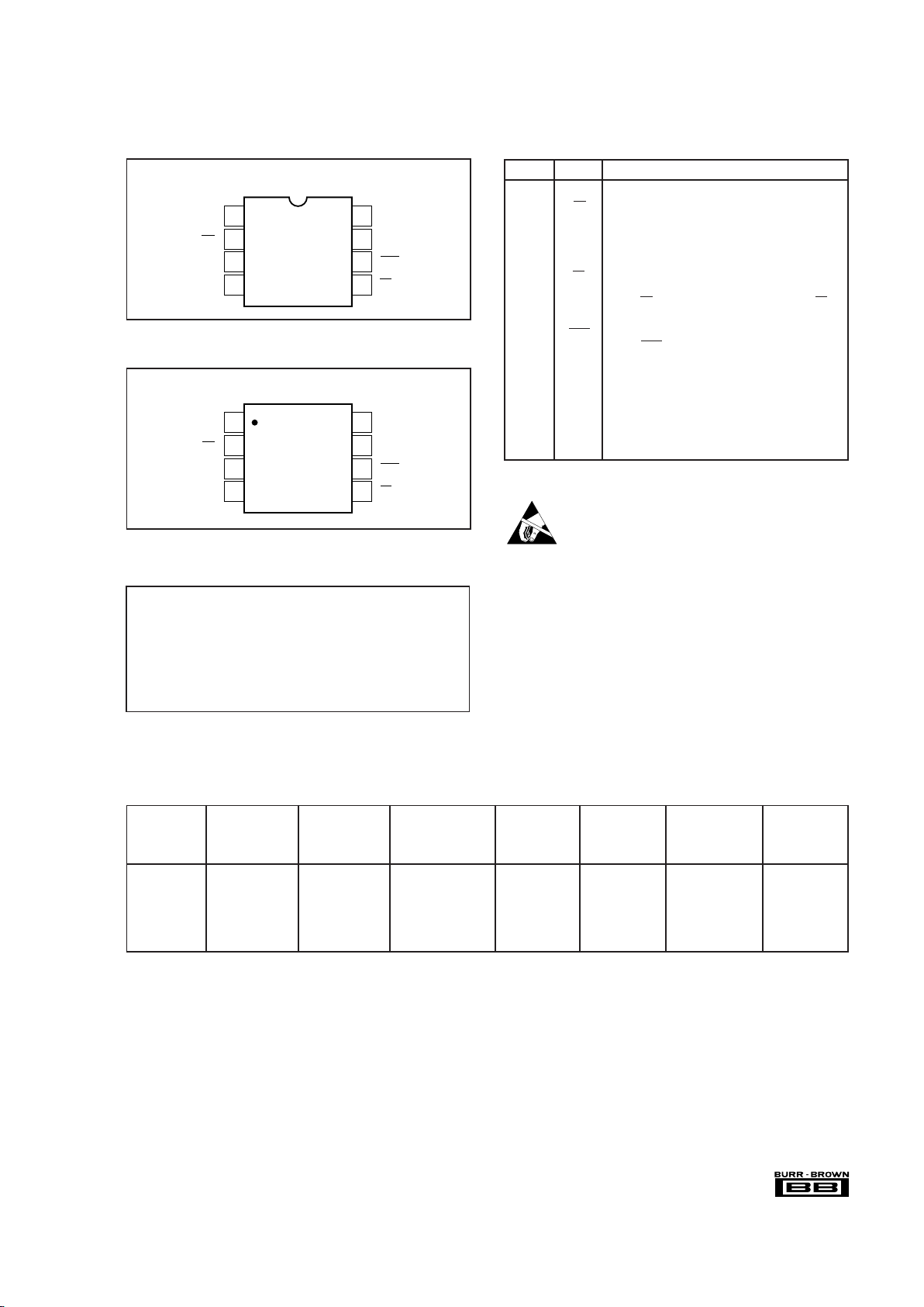
PIN CONFIGURATION
Top View DIP
PIN CONFIGURATION
Top View SOIC
VDD to GND .......................................................................... –0.3V to 6V
Digital Inputs to GND ............................................. –0.3V to V
DD
+ 0.3V
V
OUT
to GND ........................................................... –0.3V to VDD + 0.3V
Power Dissipation ........................................................................ 325mW
Thermal Resistance,
θ
JA
............................................................ 150°C/W
Maximum Junction Temperature ................................................. +150°C
Operating Temperature Range ...................................... –40°C to +85°C
Storage Temperature Range ........................................ –65°C to +150°C
Lead Temperature (soldering, 10s)............................................. +300°C
NOTE: (1) Stresses above those listed under “Absolute Maximum Ratings”
may cause permanent damage to the device. Exposure to absolute maximum
conditions for extended periods may affect device reliability.
ABSOLUTE MAXIMUM RATINGS
(1)
1
2
3
4
8
7
6
5
V
DD
CS
CLK
SDI
V
OUT
GND
CLR
LD
DAC7611
PIN DESCRIPTION
PIN LABEL DESCRIPTION
1V
DD
Power Supply
2 CS Chip Select (active LOW).
3 CLK Synchronous Clock for the Serial Data Input.
4 SDI Serial Data Input. Data is clocked into the internal
serial register on the rising edge of CLK.
5 LD Loads the Internal DAC Register. NOTE: The DAC
register is a transparent latch and is transparent
when LD is LOW (regardless of the state of CS or
CLK).
6 CLR Asynchronous Input to Clear the DAC Register.
When CLR is strobbed LOW, the DAC register is set
to 000
H
and the output voltage to 0V.
7 GND Ground
8V
OUT
Voltage Output. Fixed output voltage range of approximately 0V to 4.095V (1mV/LSB). The internal
reference maintains this output range over time,
temperature, and power supply variations (within
the values defined in the specifications section).
ELECTROSTATIC
DISCHARGE SENSITIVITY
This integrated circuit can be damaged by ESD. Burr-Brown
recommends that all integrated circuits be handled with
appropriate precautions. Failure to observe proper handling
and installation procedures can cause damage.
ESD damage can range from subtle performance degradation to complete device failure. Precision integrated circuits
may be more susceptible to damage because very small
parametric changes could cause the device not to meet its
published specifications.
PACKAGE/ORDERING INFORMATION
MINIMUM
RELATIVE DIFFERENTIAL SPECIFICATION PACKAGE
ACCURACY NONLINEARITY TEMPERATURE DRAWING ORDERING TRANSPORT
PRODUCT (LSB) (LSB) RANGE PACKAGE NUMBER
(1)
NUMBER
(2)
MEDIA
DAC7611P ±2 ±1 –40°C to +85°C 8-Pin DIP 006 DAC7611P Rails
DAC7611U ±2 ±1 –40 °C to +85°C 8-Lead SOIC 182 DAC7611U Rails
"" " " ""DAC7611U/2K5 Tape and Reel
DAC7611PB ±1 ±1 –40°C to +85°C 8-Pin DIP 006 DAC7611PB Rails
DAC7611UB ±1 ±1 –40 °C to +85°C 8-Lead SOIC 182 DAC7611UB Rails
"" " " ""DAC7611UB/2K5 Tape and Reel
NOTES: (1) For detailed drawing and dimension table, please see end of data sheet, or Appendix C of Burr-Brown IC Data Book. (2) Models with a slash (/) are
available only in Tape and Reel in the quantities indicated (e.g., /2K5 indicates 2500 devices per reel). Ordering 2500 pieces of “DAC7611/2K5” will get a single
2500-piece Tape and Reel. For detailed Tape and Reel mechanical information, refer to Appendix B of Burr-Brown IC Data Book.
Page 4
®
4
DAC7611
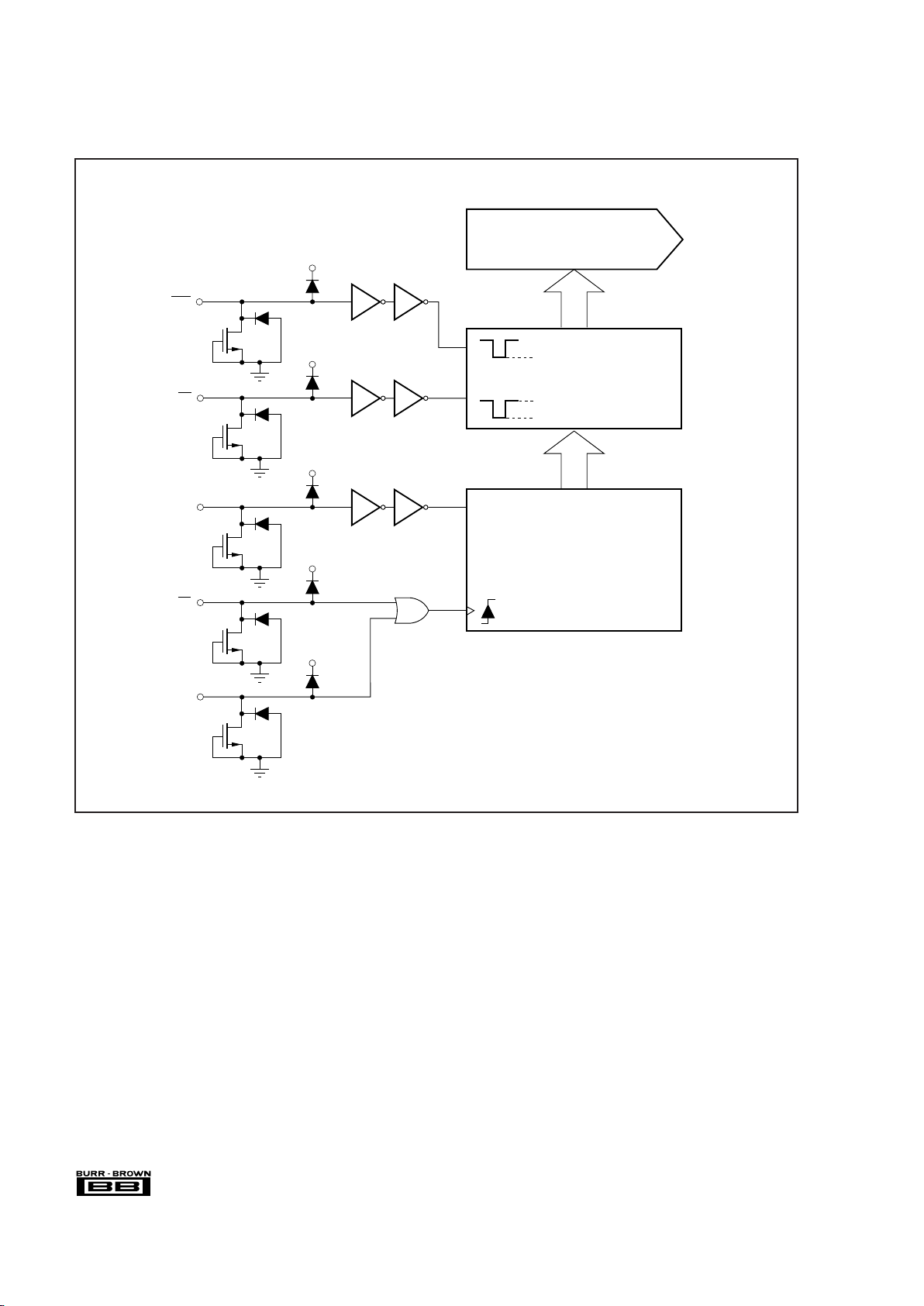
EQUIVALENT INPUT LOGIC
DAC
Register
Serial Shift Register
DAC
Switches
Force to 000
H
Transparent
Latched
Data
12
12
ESD protection
diodes to V
DD
and GND
CLR
LD
SDI
CS
CLK
Page 5

®
5
DAC7611
TIMING DIAGRAMS
LOGIC TRUTH TABLE
SERIAL SHIFT
CS
(1)
CLK
(1)
CLR LD REGISTER DAC REGISTER
H X H H No Change No Change
L L H H No Change No Change
L H H H No Change No Change
L ↑ H H Advanced One Bit No Change
↑ L H H Advanced One Bit No Change
H
(2)
XH↓No Change Changes to Value of
Serial Shift Register
H
(2)
XHL
(3)
No Change Transparent
H X L X No Change Loaded with 000
H
HX↑H No Change Latched with 000
H
↑ Positive Logic Transition; ↓ Negative Logic Transition; X = Don’t Care.
NOTES: (1) CS and CLK are interchangeable. (2) A HIGH value is suggested
in order to avoid to “false clock” from advancing the shift register and changing
the DAC voltage. (3) If data is clocked into the serial register while LD is LOW,
the DAC output voltage will change, reflecting the current value of the serial
shift register.
TIMING SPECIFICATIONS
TA = –40°C to +85°C and VDD = +5V.
SYMBOL DESCRIPTION MIN TYP MAX UNITS
t
CH
Clock Width HIGH 30 ns
t
CL
Clock Width LOW 30 ns
t
LDW
Load Pulse Width 20 ns
t
DS
Data Setup 15 ns
t
DH
Data Hold 15 ns
t
CLRW
Clear Pulse Width 30 ns
t
LD1
Load Setup 15 ns
t
LD2
Load Hold 10 ns
t
CSS
Select 30 ns
t
CSH
Deselect 20 ns
NOTE: All input control signals are specified with t
R
= tF = 5ns (10% to 90%
of +5V) and timed from a voltage level of 1.6V. These parameters are
guaranteed by design and are not subject to production testing.
D11
(MSB) (LSB)
SDI
CLK
CS
LD
D10 D9 D8 D7 D6 D5 D4 D3 D2 D1 D0
t
CSS
t
LD1
t
LD2
t
CSH
LD
FS
ZS
CLR
V
OUT
t
LDW
t
S
t
CLRW
t
S
±1 LSB
Error Band
SDI
CLK
t
CL
t
CH
t
DH
t
DS
Page 6

®
6
DAC7611
TYPICAL PERFORMANCE CURVES
At TA = +25°, and VDD = 5V, unless otherwise specified.
5
4
3
2
1
0
OUTPUT SWING vs LOAD
Output Voltage (V)
Load Resistance (Ω)
10 100 1k 10k 100k
RL tied to +5V
Data = 000
H
RL tied to AGND
Data = FFF
H
BROADBAND NOISE
Noise Voltage (500µV/div)
Time (2ms/div)
Code = FFF
H
BW = 2MHz
4.0
3.2
2.4
1.6
0.8
0
SUPPLY CURRENT vs LOGIC INPUT VOLTAGE
Supply Current (mA)
Logic Voltage (V)
0 0.5 1.0 1.5 2.0 2.5 3.0 3.5 4.0 4.5 5.0
No Load
70
60
50
40
30
20
10
0
POWER SUPPLY REJECTION vs FREQUENCY
PSR (dB)
Frequency (Hz)
10 100 1k 10k 100k 1M
Data = FFF
H
VDD = 5V
±200mV AC
5.0
4.8
4.6
4.4
4.2
4.0
MINIMUM SUPPLY VOLTAGE vs LOAD
V
DD
Minimum (V)
Output Load Current (mA)
0.010 0.100 1.000 10.000
∆VFS = 1 LSB
Data = FFF
H
1k
100
10
1
0.1
0.01
PULL-DOWN VOLTAGE vs OUTPUT SINK CURRENT
Delta V
OUT
(mV)
Current (mA)
0.001 0.01 0.1 1 10 100
85°C (mV)
–40°C
Data = 000
H
25°C
Page 7

®
7
DAC7611
TYPICAL PERFORMANCE CURVES (CONT)
At TA = +25°, and VDD = 5V, unless otherwise specified.
4.0
3.5
3.0
2.5
2.0
1.5
1.0
0.5
0
SUPPLY CURRENT vs TEMPERATURE
Supply Current (mA)
Temperature (°C)
–50 –25 0 25 50 75 100 125
V
LOGIC
= 2.4V
Data = FFF
H
No Load
VDD = 4.75V
VDD = 5.0V
VDD = 5.25V
RISE TIME DETAIL
Output Voltage (1mV/div)
Time (10µs/div)
LD
V
OUT
LARGE-SIGNAL SETTLING TIME
1V/div
Time (20µs/div)
CL = 110pF
R
L
= No Load
LD
V
OUT
80
60
40
20
0
–20
–40
–60
–80
SHORT-CIRCUIT CURRENT vs OUTPUT VOLTAGE
Output Current (mA)
Output Voltage (V)
0 0.5 1.0 1.5 2.0 2.5 3.0 3.5 4.0 4.5 5.0
Positive
Current
Limit
Data = 800
H
Output tied to I
SOURCE
Negative
Current
Limit
MIDSCALE GLITCH PERFORMANCE
V
OUT
(10mV/div)
Time (500ns/div)
LD
V
OUT
7FFH to 800
H
MIDSCALE GLITCH PERFORMANCE
V
OUT
(10mV/div)
Time (500ns/div)
LD
V
OUT
800H to 7FF
H
Page 8

®
8
DAC7611
TYPICAL PERFORMANCE CURVES (CONT)
At TA = +25°, and VDD = 5V, unless otherwise specified.
3
2
1
0
–1
ZERO-SCALE VOLTAGE vs TEMPERATURE
Zero-Scale (mV)
Temperature (°C)
–50 0 25–25 50 75 100 125
FALL TIME DETAIL
Output Voltage (1mV/div)
Time (10µs/div)
LD
V
OUT
10.000
1.000
0.100
0.010
OUTPUT VOLTAGE NOISE vs FREQUENCY
Noise (µV/√Hz)
Frequency (Hz)
10 100 1k 10k 100k
Data = FFF
H
5
4
3
2
1
0
–1
–2
–3
–4
–5
Output Voltage Change (mV)
Hours of Operation at +150°C
LONG-TERM DRIFT ACCELERATED BY BURN-IN
0 400200 600 800 1000 1200
avg
max
min
120 Units
0
10
20
30
40
50
60
–12
–8 –4 0 4 8 12
T.U.E = ΣINL = ZS + FS
Sample Size = 300 Units
T
A
= +25°C
Number of Units
TOTAL UNADJUSTED ERROR HISTOGRAM
4.115
4.110
4.105
4.100
4.095
4.090
4.085
4.080
4.075
FULL-SCALE VOLTAGE vs TEMPERATURE
Full-Scale Output (V)
Temperature (°C)
–50 0 25–25 50 75 100 125
No Load
Sample Size = 300
Avg + 3σ
Avg – 3σ
Avg
Page 9

®
9
DAC7611
TYPICAL PERFORMANCE CURVES (CONT)
At TA = +25°, and VDD = 5V, unless otherwise specified.
LINEARITY ERROR vs DIGITAL CODE
(at +85°C)
Linearity Error (LSBs)
0
2.0
1.5
1.0
0.5
0
–0.5
–1.0
–1.5
–2.0
512 1024 1536 2048 2560 3072 3584 4096
Code
LINEARITY ERROR vs DIGITAL CODE
(at +25°C)
Linearity Error (LSBs)
0
2.0
1.5
1.0
0.5
0
–0.5
–1.0
–1.5
–2.0
512 1024 1536 2048 2560 3072 3584 4096
Code
LINEARITY ERROR vs DIGITAL CODE
(at –40°C)
Linearity Error (LSBs)
0
2.0
1.5
1.0
0.5
0
–0.5
–1.0
–1.5
–2.0
512 1024 1536 2048 2560 3072 3584 4096
Code
Page 10

®
10
DAC7611
clear input (CLR) is provided to simplify start-up or periodic
resets. Table I shows the relationship between input code
and output voltage.
The digital data into the DAC7611 is double-buffered. This
means that new data can be entered into the DAC without
disturbing the old data and the analog output of the converter. At some point after the data has been entered into the
serial shift register, this data can be transferred into the DAC
register. This transfer is accomplished with a HIGH to LOW
transition of the LD pin. However, the LD pin makes the
DAC register transparent. If new data is shifted into the shift
register while LD is LOW, the DAC output voltage will
change as each new bit is entered. To prevent this, LD must
be returned HIGH prior to shifting in new serial data.
At any time, the contents of the DAC register can be set to
000
H
(analog output equals 0V) by taking the CLR input
LOW. The DAC register will remain at this value until CLR
is returned HIGH and LD is taken LOW to allow the
contents of the shift register to be transferred to the DAC
register. If LD is LOW when CLR is taken LOW, the DAC
register will be set to 000
H
and the analog output driven to
0V. When CLR is returned HIGH, the DAC register will be
set to the current value in the serial shift register and the
analog output will respond accordingly.
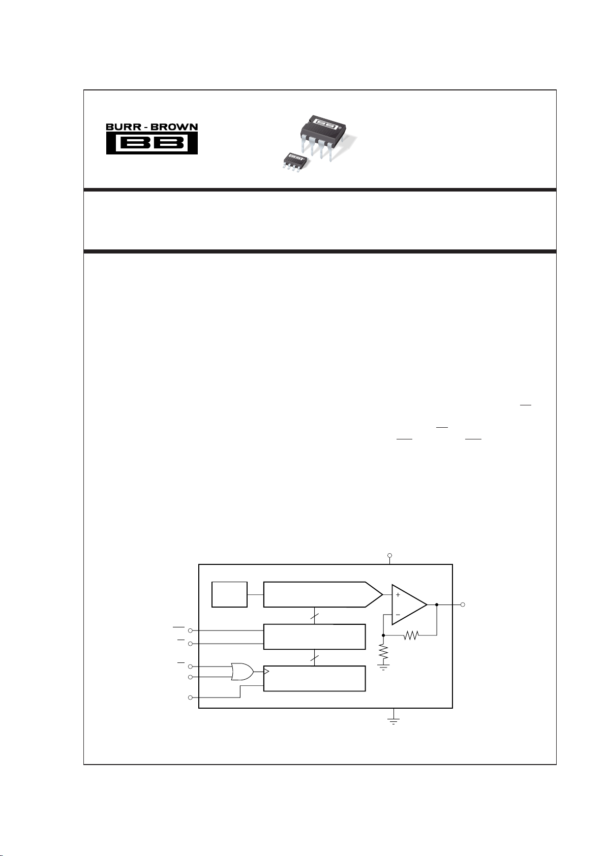
DIGITAL-TO-ANALOG CONVERTER
The internal DAC section is a 12-bit voltage output
device that swings between ground and the internal reference voltage. The DAC is realized by a laser-trimmed
R-2R ladder network which is switched by N-channel
MOSFETs. The DAC output is internally connected to
the rail-to-rail output operational amplifier.
OUTPUT AMPLIFIER
A precision, low-power amplifier buffers the output of the
DAC section and provides additional gain to achieve a 0 to
4.095V range. The amplifier has low offset voltage, low
noise, and a set gain of 1.682V/V (4.095/2.435). See Figure
2 for an equivalent circuit schematic of the analog portion of
the DAC7611.
FIGURE 2. Simplified Schematic of Analog Portion.
OPERATION
The DAC7611 is a 12-bit digital-to-analog converter (DAC)
complete with a serial-to-parallel shift register, DAC register, laser-trimmed 12-bit DAC, on-board reference, and a
rail-to-rail output amplifier. Figure 1 shows the basic operation of the DAC7611.
INTERFACE
Figure 1 shows the basic connection between a
microcontroller and the DAC7611. The interface consists of
a serial clock (CLK), serial data (SDI), and a load strobe
signal (LD). In addition, a chip select (CS) input is available
to enable serial communication when there are multiple
serial devices. The data format is Straight Binary and is
loaded MSB-first into the shift registers. An asynchronous
DAC7611 Full-Scale Range = 4.095V
Least Significant Bit = 1mV
DIGITAL INPUT CODE ANALOG OUTPUT
STRAIGHT BINARY (V) DESCRIPTION
FFF
H
+4.095 Full Scale
801
H
+2.049 Midscale + 1 LSB
800
H
+2.048 Midscale
7FF
H
+2.047 Midscale – 1 LSB
000
H
0 Zero Scale
TABLE I. Digital Input Code and Corresponding Ideal
Analog Output.
FIGURE 1. Basic Operation of the DAC7611.
2R
2R
2R
R
2R
2R
R
R1
R
R2
Output Amplifier
R-2R DAC
Bandgap
Reference
2.435V
Buffer
1
2
3
4
8
7
6
5
V
OUT
GND
CLR
LD
V
DD
CS
CLK
SDI
Serial Clock
Serial Data
Load Strobe
DAC7611
+
0.1µF10µF
From
µC
0V to
+4.095V
+5V
Page 11

®
11
DAC7611
The output amplifier has a 7µs typical settling time to ±1
LSB of the final value. Note that there are differences in the
settling time for negative-going signals versus positivegoing signals.
The rail-to-rail output stage of the amplifier provides the
full-scale range of 0V to 4.095V while operating on a supply
voltage as low as 4.75V. In addition to its ability to drive
resistive loads, the amplifier will remain stable while driving
capacitive loads of up to 500pF. See Figure 3 for an equivalent circuit schematic of the amplifier’s output driver and the
Typical Performance Curves section for more information
regarding settling time, load driving capability, and output
noise.
The DAC7611 power supply should be bypassed as shown
in Figure 1. The bypass capacitors should be placed as close
to the device as possible, with the 0.1uF capacitor taking
priority in this regard. The Power Supply Rejection vs
Frequency graph in the Typical Performance Curves section
shows the PSRR performance of the DAC7611. This should
be taken into account when using switching power supplies
or DC/DC converters.
In addition to offering guaranteed performance with V
DD
in
the 4.75V to 5.25V range, the DAC7611 will operate with
reduced performance down to 4.5V. Operation between
4.5V and 4.75V will result in longer settling time, reduced
performance, and current sourcing capability. Consult the
V
DD
vs Load Current graph in the Typical Performance
Curves section for more information.
APPLICATIONS
POWER AND GROUNDING
The DAC7611 can be used in a wide variety of situations—
from low power, battery operated systems to large-scale
industrial process control systems. In addition, some applications require better performance than others, or are particularly sensitive to one or two specific parameters. This
diversity makes it difficult to define definite rules to follow
concerning the power supply, bypassing, and grounding.
The following discussion must be considered in relation to
the desired performance and needs of the particular system.
A precision analog component requires careful layout, adequate bypassing, and a clean, well-regulated power supply.
As the DAC7611 is a single-supply, +5V component, it will
often be used in conjunction with digital logic,
microcontrollers, microprocessors, and digital signal processors. The more digital logic present in the design and the
higher the switching speed, the more difficult it will be to
achieve good performance.
Because the DAC7611 has a single ground pin, all return
currents, including digital and analog return currents, must
flow through this pin. The GND pin is also the ground
reference point for the internal bandgap reference. Ideally,
GND would be connected directly to an analog ground
plane. This plane would be separate from the ground connection for the digital components until they are connected
at the power entry point of the system (see Figure 4).
The power applied to V
DD
should be well regulated and lownoise. Switching power supplies and DC/DC converters will
often have high-frequency glitches or spikes riding on the
output voltage. In addition, digital components can create
similar high frequency spikes as their internal logic switches
states. This noise can easily couple into the DAC output
voltage through various paths between VDD and V
OUT
.
N-Channel
P-Channel
V
DD
V
OUT
AGND
FIGURE 3. Simplified Driver Section of Output Amplifier.
POWER SUPPLY
A BiCMOS process and careful design of the bipolar and
CMOS sections of the DAC7611 result in a very low power
device. Bipolar transistors are used where tight matching
and low noise are needed to achieve analog accuracy, and
CMOS transistors are used for logic, switching functions
and for other low power stages.
If power consumption is critical, it is important to keep the
logic levels on the digital inputs (SDI, CLK, CS, LD, CLR)
as close as possible to either VDD or ground. This will keep
the CMOS inputs (see “Supply Current vs Logic Input
Voltages” in the Typical Performance Curves) from shunting current between V
DD
and ground. Thus, CMOS logic
levels rather than TTL logic levels, are strongly recommended for driving the DAC7611.
Page 12

®
12
DAC7611
As with the GND connection, VDD should be connected to
a +5V power supply plane or trace that is separate from the
connection for digital logic until they are connected at the
power entry point. In addition, the 10µF and 0.1µF capacitors shown in Figure 4 are strongly recommended and
should be installed as close to V
DD
and ground as possible.
In some situations, additional bypassing may be required
such as a 100µF electrolytic capacitor or even a “Pi” filter
made up of inductors and capacitors—all designed to essentially lowpass filter the +5V supply, removing the high
frequency noise (see Figure 4).
OFFSET ERROR MEASUREMENT
As with most DACs, the DAC7611 can have an offset error
(or zero scale error) which is either negative or positive. If
the error is positive, the output voltage for an input code of
000
H
will be greater than 0V. If the error is negative, the
output voltage is below 0V. However, since the DAC7611 is
a single-supply device and cannot swing below ground, the
output voltage will be 0V, giving the impression that the
offset error is zero.
Since measuring the offset error on a DAC is such a
common task, a method is needed to reliably measure the
offset error of the DAC7611. This can easily be done as
shown in Figure 5. The resistor between V
OUT
and a negative voltage provides the output amplifier some ability to
swing below ground.
FIGURE 4. Suggested Power and Ground Connections for a DAC7611 Sharing a +5V Supply with a Digital System.
FIGURE 5. Offset Error Measurement Circuit.
+
+5V
GND
100µF
Digital Circuits
+5V
GND
+5V
Power
Supply
Other
Analog
Components
V
DD
GND
DAC7611
+
10µF
0.1µF
Optional
1
2
3
4
8
7
6
5
V
OUT
GND
CLR
LD
V
DD
CS
CLK
SDI
DAC7611
+
0.1µF10µF
+5V
R
i
≤ 200µA
–V
 Loading...