

Datasheet DAC7541AKU-1K, DAC7541AKU, DAC7541AKP, DAC7541AJU, DAC7541AJP Datasheet (Burr Brown Corporation)
Page 1
®
DAC7541A
Low Cost 12-Bit CMOS
Four-Quadrant Multiplying
DIGITAL-TO-ANALOG CONVERTER
FEATURES
● FULL FOUR-QUADRANT
MULTIPLICATION
● 12-BIT END-POINT LINEARITY
● DIFFERENTIAL LINEARITY
OVER TEMPERATURE
● MONOTONICITY GUARANTEED OVER
TEMPERATURE
● TTL-/CMOS-COMPATIBLE
● SINGLE +5V TO +15V SUPPLY
● LATCH-UP RESISTANT
● 7521/7541/7541A REPLACEMENT
● PACKAGES: Plastic DIP, Plastic SOIC
● LOW COST
V
REF
±1/2LSB MAX
10kΩ 10kΩ
20kΩ 20kΩ
10kΩ
20kΩ
DESCRIPTION
The Burr-Brown DAC7541A is a low cost 12-bit,
four-quadrant multiplying digital-to-analog converter.
Laser-trimmed thin-film resistors on a monolithic
CMOS circuit provide true 12-bit integral and differential linearity over the full specified temperature
range.
DAC7541A is a direct, improved pin-for-pin replacement for 7521, 7541, and 7541A industry standard
parts. In addition to a standard 18-pin plastic package,
the DAC7541A is also available in a surface-mount
plastic 18-pin SOIC.
10kΩ
20kΩ
20kΩ
20kΩ
SPDT NMOS
Switches
(MSB)
Digital Inputs (DTL-/TTL-/CMOS-compatible)
Logic: A switch is closed to I
International Airport Industrial Park • Mailing Address: PO Box 11400 • Tucson, AZ 85734 • Street Address: 6730 S. Tucson Blvd. • Tucson, AZ 85706
Tel: (520) 746-1111 • Twx: 910-952-1111 • Cable: BBRCORP • Telex: 066-6491 • FAX: (520) 889-1510 • Immediate Product Info: (800) 548-6132
©
1987 Burr-Brown Corporation PDS-639C Printed in U.S.A. September, 1993
for its digital input in a “HIGH” state.
OUT 1
Bit 3Bit 2Bit 1
Bit 11
Bit 12
(LSB)
Switches shown for digital inputs “HIGH”.
10kΩ
I
OUT 2
I
OUT 1
R
FB
Page 2
SPECIFICATIONS
ELECTRICAL
At +25°C, +V
PARAMETER GRADE TA = +25°C
ACCURACY
Resolution All 12 12 Bits
Relative Accuracy J ±1 ±1 LSB max ±1LSB = ±0.024% of FSR.
Differential Non-linearity J ±1 ±1 LSB max All grades guaranteed monotonic to 12 bits,
Gain Error J ±6 ±8 LSB max Measured using internal R
Gain Temperature Coefficient
(∆Gain/∆Temperature) ALL 5 ppm/°C max Typical value is 2ppm/°C.
Output Leakage Current: Out
REFERENCE INPUT
Voltage (Pin 17 to GND) All –10/+10 –10/+10 V min/max
Input Resistance (Pin 17 to GND) All 7-18 7-18 kΩ min/max
DIGITAL INPUTS
V
(Input HIGH Voltage) All 2.4 2.4 V min
IN
V
(Input LOW Voltage) All 0.8 0.8 V max
IL
I
(Input Current) All ±1 ±1 µA max Logic inputs are MOS gates.
IN
C
(Input Capacitance)
IN
POWER SUPPLY REJECTION
∆Gain/∆V
POWER SUPPLY
Range All +5 to +16 +5 to +16 V min to Accuracy is not guaranteed over this range.
V
DD
I
DD
NOTES: (1) Temperature ranges are: = 0°C to + 70°C for JP, KP, JU and KU versions. (2) Guaranteed by design but not production tested.
= +12V or +15V, V
DD
DD
= +10V, V
REF
PIN 1
= V
= 0V, unless otherwise specified.
PIN 2
DAC7541A
MAX
(1)
, T
MIN
UNITS TEST CONDITIONS/COMMENTS
TA = T
K ±1/2 ±1/2 LSB max ±1/2LSB = ±0.012% of FSR.
K ±1/2 ±1/2 LSB max T
MIN
to T
K ±1 ±3 LSB max of leakage current and gain T.C.
Gain error can be trimmed to zero.
(Pin 1) J, K ±5 ±10 nA max All digital inputs = 0V.
1
Out
(Pin 2) J, K ±5 ±10 nA max All digital inputs = VDD.
2
Typical input resistance = 11kΩ.
Typical input resistance temperature coefficient is
–50ppm/°C.
I
typ (25°C) = 1nA
(2)
All 8 8 pF max VIN = 0V
IN
All ±0.01 ±0.02 % per % max VDD = +11.4V to +16V
V max
All 2 2 mA max All digital inputs VIL or VIN.
All 100 500 µA max All digital inputs 0V or V
MAX
.
and includes effect
FB
.
DD
AC PERFORMANCE CHARACTERISTICS
These characteristics are included for design guidance only and are not production tested.
V
= +15V, V
DD
PARAMETER GRADE TA = +25°C
PROPAGATION DELAY
(from Digital Input change to 90% of Out
final Analog Output) All 100 — ns typ Digital Inputs = 0V to V
DIGITAL-TO-ANALOG GLITCH V
IMPULSE All 1000 — nV-s typ 0V. Measured using OPA606 as output amplifier.
MULTIPLYING FEEDTHROUGH
ERROR
(V
to Out1) All 1.0 — mVp-p max V
REF
OUTPUT CURRENT SETTLING TIME
OUTPUT CAPACITANCE
C
OUT 1
C
OUT 2
C
OUT 1
C
OUT 2
NOTE: (1) Temperature ranges are: = 0°C to + 70°C for JP, KP, JU and KU versions.
= +10V except where stated, V
REF
PIN 1
= V
= 0V, output amp is OPA606 except where stated.
PIN 2
DAC7541A
MAX
(1)
, T
MIN
UNITS TEST CONDITIONS/COMMENTS
Load = 100Ω, C
1
= 0V, all digital inputs 0V to VDD or VDD to
REF
= ±10V, 10kHz sine wave.
REF
TA = T
All 0.6 — µs typ To 0.01% of Full Scale Range.
Out
Load = 100Ω, C
All 1.0 — µs max Digital Inputs: 0V to V
1
(Pin 1) All 100 100 pF max Digital Inputs = V
(Pin 2) All 60 60 pF max Digital Inputs = V
(Pin 1) All 70 70 pF max Digital Inputs = V
(Pin 2) All 100 100 pF max Digital Inputs = V
®
DAC7541A
2
IH
IH
IL
IL
= 13pF.
EXT
or VDD to 0V.
DD
= 13pF.
EXT
or VDD to 0V.
DD
Page 3
ABSOLUTE MAXIMUM RATINGS
DAC7541A
1
2
3
4
5
6
7
8
9
18
17
16
15
14
13
12
11
10
I
OUT 1
I
OUT 2
GND
Bit 1 (MSB)
Bit 2
Bit 3
Bit 4
Bit 5
Bit 6
R
FB
V
REF
+VDD
Bit 12
(LSB)
Bit 11
Bit 10
Bit 9
Bit 8
Bit 7
VDD (Pin 16) to Ground ...................................................................... +17V
V
(Pin 17) to Ground ..................................................................... +25V
REF
V
(Pin 18) to Ground..................................................................... ±25V
RPB
Digital Input Voltage (pins 4-15) to Ground...............................–0.4V, V
V
, V
PIN 1
Power Dissipation (any Package):
To +75°C..................................................................................... 450mW
Derates above +75°C ..............................................................–6mW/°C
Lead Temperature (soldering, 10s)................................................ +300°C
Storage Temperature: Plastic Package ......................................... +125°C
NOTE: (1) Stresses above those listed above may cause permanent damage to
the device. This is a stress rating only and functional operation of the device at
these or any other condition above those indicated in the operational sections of
this specification is not implied. Exposure to absolute maximum rating conditions
for extended periods may affect device reliability.
to Ground ............................................................. –0.4V, V
PIN 2
(1)
DD
DD
ELECTROSTATIC
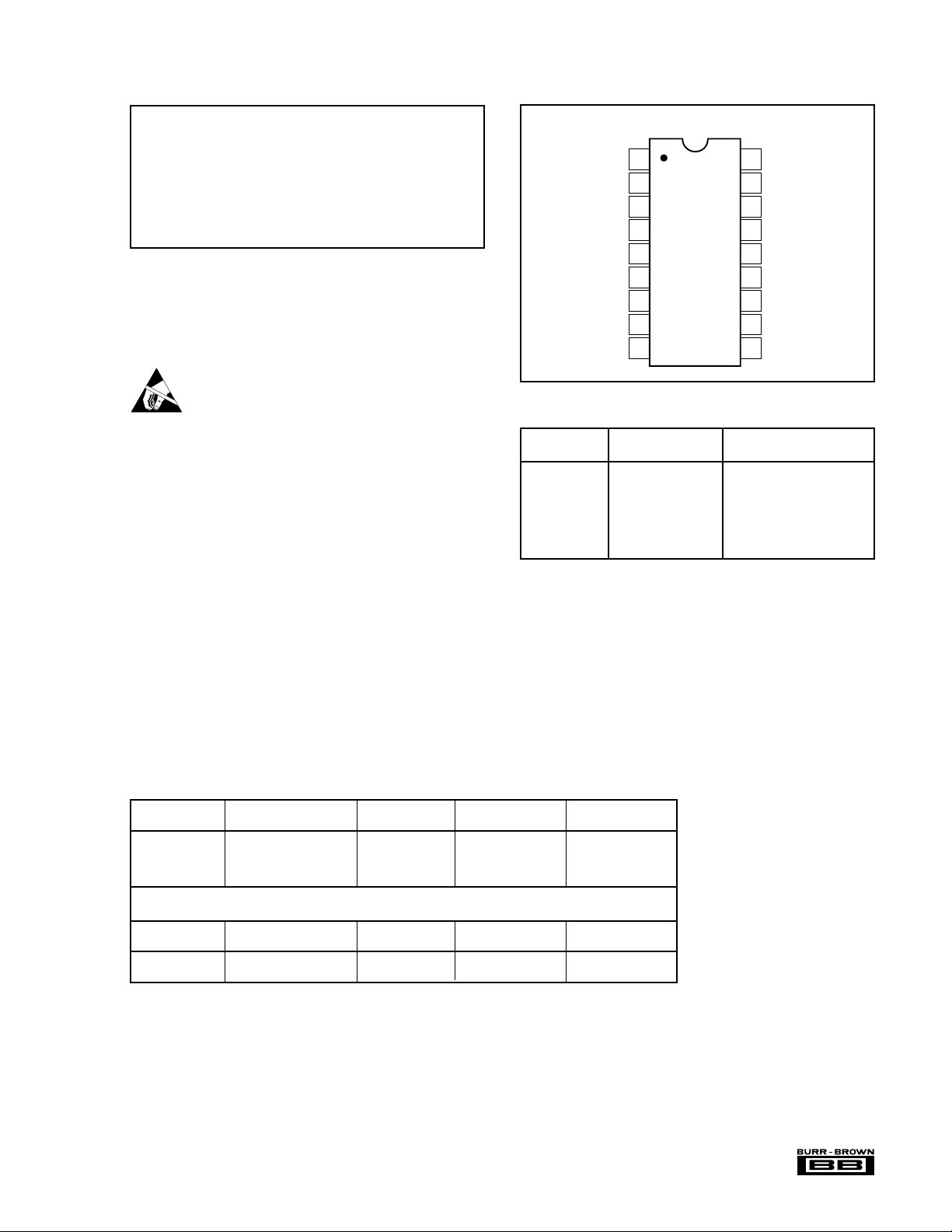
PIN CONNECTIONS
Top View DIP/SOIC
DISCHARGE SENSITIVITY
PACKAGE INFORMATION
The DAC7541A is an ESD (electrostatic discharge) sensitive device. The digital control inputs have a special FET
structure, which turns on when the input exceeds the supply
by 18V, to minimize ESD damage. However, permanent
damage may occur on unconnected devices subject to high
energy electrostatic fields. When not in use, devices must be
stored in conductive foam or shunts. The protective foam
should be discharged to the destination socket before
devices are removed.
MODEL PACKAGE NUMBER
DAC7541JP Plastic DIP 218
DAC7541KP Plastic DIP 218
DAC7541JU Plastic SOIC 219
DAC7541KU Plastic SOIC 219
DAC7541JP-BI Plastic DIP 218
DAC7541KP-BI Plastic DIP 218
NOTE: (1) For detailed drawing and dimension table, please see end of data
sheet, or Appendix D of Burr-Brown IC Data Book.
BURN-IN SCREENING
Burn-in screening is an option available for the models in the
Ordering Information table. Burn-in duration is 160 hours at
the indicated temperature (or equivalent combination of time
and temperature).
All units are tested after burn-in to ensure that grade specifications are met. To order burn-in, add “-BI” to the base
model number.
ORDERING INFORMATION
MODEL PACKAGE RANGE ACCURACY (LSB) GAIN ERROR (LSB)
DAC7541AJP Plastic DIP 0° C to +70°C ±1 ±6
DAC7541AKP Plastic DIP 0°C to +70°C ±1/2 ±1
DAC7541AJU Plastic SOIC 0°C to +70°C ±1 ±6
DAC7541AKU Plastic SOIC 0°C to +70°C ±1/2 ±1
BURN-IN SCREENING OPTION
See text for details.
MODEL PACKAGE RANGE ACCURACY (LSB) (160 Hours)
DAC7541AJP-BI Plastic DIP 0°C to +70°C ±1 +85°C
DAC7541AKP-BI Plastic DIP 0°C to +70°C ±1/2 +85°C
TEMPERATURE RELATIVE
TEMPERATURE RELATIVE BURN-IN TEMP.
PACKAGE DRAWING
(1)
(1)
The information provided herein is believed to be reliable; however, BURR-BROWN assumes no responsibility for inaccuracies or omissions. BURR-BROWN
assumes no responsibility for the use of this information, and all use of such information shall be entirely at the user’s own risk. Prices and specifications are subject
to change without notice. No patent rights or licenses to any of the circuits described herein are implied or granted to any third party. BURR-BROWN does not
authorize or warrant any BURR-BROWN product for use in life support devices and/or systems.
®
3
DAC7541A
Page 4

DIE TOPOLOGY DAC7541A
TYPICAL PERFORMANCE CURVES
TA = +25°C, VDD = +15V, unless otherwise noted.
PAD FUNCTION
1I
2I
3 GND
4 Bit 1 (MSB)
5 Bit 2
6 Bit 3
7 Bit 4
8 Bit 5
9 Bit 6
Substrate Bias: Isolated.
NC: No Connection.
OUT1
OUT2
PAD FUNCTION
10 Bit 7
11 Bit 8
12 Bit 9
13 Bit 10
14 Bit 11
15 Bit 12 (LSB)
16 +V
17 V
18 R
DD
REF
FEEDBACK
MECHANICAL INFORMATION
MILS (0.001") MILLIMETERS
Die Size 104 x 105 ±5 2.64 x 2.67 ±0.13
Die Thickness 20 ±3 0.51 ±0.08
Min. Pad Size 4 x 4 0.10 x 0.10
Metalization Aluminum
3
5/2
2
3/2
1
Gain Error (LSB)
1/2
0
015
3/2
5/4
1
3/4
1/2
Linearity Error (LSB)
1/4
0
015
GAIN ERROR vs SUPPLY VOLTAGE
510
Supply Voltage (V)
LINEARITY vs SUPPLY VOLTAGE
510
Supply Voltage (V)
10
1
0.10
Feedthrough (% FSR)
0.010
0.001
3/2
5/4
1
3/4
1/2
Supply Current (µA)
1/4
0
FEEDTHROUGH ERROR vs FREQUENCY
1k 10k100 100k
SUPPLY CURRENT vs SUPPLY VOLTAGE
015
510
Frequency (Hz)
Supply Voltage (V)
1M
V
= +2.4V
IH
V
= V
IH
DD
®
DAC7541A
4
Page 5

DISCUSSION
Bit 12
(LSB)
10kΩ 10kΩ
20kΩ 20kΩ
10kΩ
20kΩ
20kΩ
I
OUT 2
Bit 3Bit 2Bit 1
(MSB)
V
REF
20kΩ
I
OUT 1
R
FB
Digital Inputs (DTL-/TTL-/CMOS-compatible)
Switches shown for digital inputs “HIGH”.
S
2
S
1
S
3
S
12
OF SPECIFICATIONS
RELATIVE ACCURACY
This term (also known as linearity) describes the transfer
function of analog output to digital input code. The linearity
error describes the deviation from a straight line between
zero and full scale.
DIFFERENTIAL NONLINEARITY
Differential nonlinearity is the deviation from an ideal 1LSB
change in the output, from one adjacent output state to the
next. A differential nonlinearity specification of ±1.0LSB
guarantees monotonicity.
GAIN ERROR
Gain error is the difference in measure of full-scale output
versus the ideal DAC output. The ideal output for the
DAC7541A is –(4095/4096) X (V
adjusted to zero using external trims.
OUTPUT LEAKAGE CURRENT
The measure of current which appears at Out
loaded with all zeros, or at Out
all ones.
). Gain error may be
REF
with the DAC
with the DAC loaded with
2
1
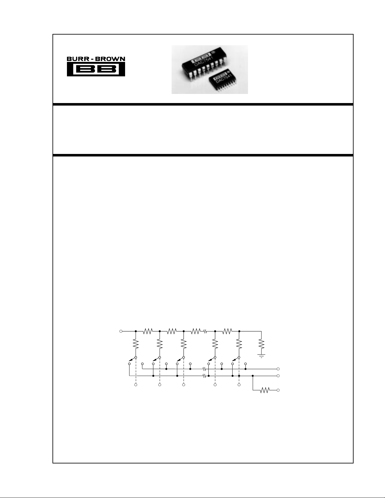
CIRCUIT DESCRIPTION
The DAC7541A is a 12-bit multiplying D/A converter
consisting of a highly stable thin-film R-2R ladder network
and 12 pairs of current steering switches on a monolithic
chip. Most applications require the addition of a voltage or
current reference and an output operational amplifier.
A simplified circuit of the DAC7541A is shown in Figure 1.
The R-2R inverted ladder binarily divides the input currents
that are switched between I
OUT 1
and I
switching allows a constant current to be maintained in each
ladder leg independent of the input code.
The input resistance at V
R
(R
LDR
is the R/2R ladder characteristic resistance and
LDR
is equal to value “R”). Since R
(Figure 1) is always equal to
REF
at the V
IN
the reference terminal can be driven by a reference voltage
or a reference current, AC or DC, of positive or negative
polarity.
bus lines. This
OUT 2
pin is constant,
REF
MULTIPLYING FEEDTHROUGH ERROR
This is the AC error output due to capacitive feedthrough
from V
to Out1 with the DAC loaded with all zeros. This
REF
test is performed at 10kHz.
OUTPUT CURRENT SETTLING TIME
This is the time required for the output to settle to a tolerance
of ±0.5LSB of final value from a change in code of all zeros
to all ones, or all ones to all zeros.
PROPAGATION DELAY
This is the measure of the delay of the internal circuitry and
is measured as the time from a digital code change to the
point at which the output reaches 90% of final value.
DIGITAL-TO-ANALOG GLITCH IMPULSE
This is the measure of the area of the glitch energy measured
in nV-seconds. Key contributions to glitch energy are digital
word-bit timing differences, internal circuitry timing differences, and charge injected from digital logic.
MONOTONICITY
Monotonicity assures that the analog output will increase or
stay the same for increasing digital input codes. The
DAC7541A is guaranteed monotonic to 12 bits.
POWER SUPPLY REJECTION
Power supply rejection is the measure of the sensitivity of
the output (full scale) to a change in the power supply
voltage.
FIGURE 1. Simplified DAC Circuit.
EQUIVALENT CIRCUIT ANALYSIS
Figures 2 and 3 show the equivalent circuits for all digital
inputs low and high, respectively. The reference current is
switched to I
inputs are high. The I
when all inputs are low and I
OUT 2
current source is the combination of
L
OUT 1
surface and junction leakages to the substrate; the
1/4096 current source represents the constant one-bit current
drain through the ladder terminal.
DYNAMIC PERFORMANCE
Output Impedance
The output resistance, as in the case of the output capacitance, is also modulated by the digital input code. The
resistance looking back into the I
terminal may be
OUT 1
anywhere between 10kΩ (the feedback resistor alone when
all digital inputs are low) and 7.5kΩ (the feedback resistor
in parallel with approximately 30kΩ of the R-2R ladder
network resistance when any single bit logic is high). The
static accuracy and dynamic performance will be affected by
this modulation. The gain and phase stability of the output
5
DAC7541A
when
®
Page 6

R
FB
R = 10kΩ
I
OUT 1
I
L
I
REF
R ≈ 10kΩ
V
REF
1/4096 I
L
60pF
90pF
I
OUT 2
I
REF
R ≈ 10kΩ
V
REF
1/4096 I
L
I
L
90pF
55pF
R
R = 10kΩ
I
I
FB
OUT 1
OUT 2
FIGURE 2. DAC7541A Equivalent Circuit (All inputs
LOW).
amplifier, board layout, and power supply decoupling will
all affect the dynamic performance of the DAC7541A. The
use of a compensation capacitor may be required when highspeed operational amplifiers are used. It may be connected
across the amplifier’s feedback resistor to provide the necessary phase compensation to critically dampen the output.
See Figures 4 and 6.
APPLICATIONS
OP AMP CONSIDERATIONS
The input bias current of the op amp flows through the
feedback resistor, creating an error voltage at the output of
the op amp. This will show up as an offset through all codes
of the transfer characteristics. A low bias current op amp
such as the OPA606 is recommended.
Low offset voltage and V
output impedance of the DAC is modulated with the digital
code. This impedance change (approximately 10kΩ to 30kΩ)
is a change in closed-loop gain to the op amp. The result is
that VOS will be multiplied by a factor of one to two
depending on the code. This shows up as a linearity error.
Offset can be adjusted out using Figure 4. Gain may be
adjusted using Figure 5.
drift are also important. The
OS
FIGURE 3. DAC7541A Equivalent Circuit (All inputs
HIGH).
BINARY INPUT ANALOG OUTPUT
MSB LSB
1111 1111 1111 –V
1000 0000 0000 –V
0000 0000 0001 –V
0000 0000 0000 0V
(4095/4096)
REF
(2048/4096)
REF
(1/4096)
REF
TABLE I. Unipolar Codes.
C
phase compensation (10 to 25pF) in Figure 4 may be
1
required for stability when using high speed amplifiers. C
is used to cancel the pole formed by the DAC internal
feedback resistance and output capacitance at Out
in Figure 5 provides full scale trim capability—load the
R
1
DAC register to 1111 1111 1111, adjust R
V
(4095/4096). Alternatively, full scale can be adjusted
REF
by omitting R
and R2 and trimming the reference voltage
1
for V
1
1
.
OUT
= –
magnitude.
BIPOLAR FOUR-QUADRANT OPERATION
Figure 6 shows the connections for bipolar four-quadrant
operation. Offset can be adjusted with the A
to A2 summing
1
resistor, with the input code set to 1000 0000 0000. Gain
may be adjusted by varying the feedback resistor of A2. The
input/output relationship is shown in Table II.
1
UNIPOLAR BINARY OPERATION
(Two-Quadrant Multiplication)
Figure 4 shows the analog circuit connections required for
unipolar binary (two-quadrant multiplication) operation. With
a DC reference voltage or current (positive or negative
polarity) applied at pin 17, the circuit is a unipolar D/A
converter. With an AC reference voltage or current, the
circuit provides two-quadrant multiplication (digitally controlled attenuation). The input/output relationship is shown
in Table I.
®
DAC7541A
BINARY INPUT ANALOG OUTPUT
MSB LSB
1111 1111 1111 +V
1000 0000 0000 0V
0111 1111 1111 –V
0000 0000 0000 –V
TABLE II. Bipolar Codes.
6
(2047/2048)
REF
(1/2048)
REF
(2048/2048)
REF
Page 7

MSB
B
•5•6•7•8•9•10•11•12•13•14B
1
4
16
+15V
17
V
REF
DAC7541A Out
Out
3
12
15
R
F
2
C
18
1
1
1
OPA604
2
V
10kΩ
V
= –V
OUT
–10V ≤ V
OUT
0 ≤ V
OUT ≤
Where: BN = 1 if the BN digital input is HIGH.
B
B
B
B
1
2
3
+ + + • • • +
(
REF
2
4
8
+10V
REF ≤
4095
– V
REF
4096
= 0 if the BN digital input is LOW.
N
Single-Point Ground
+V
CC
FIGURE 4. Basic Connection With Op Amp VOS Adjust: Unipolar (two-quadrant) Multiplying Configuration.
B
4096
12
)
MSB
B
•5•6•7•8•9•10•11•12•13•14B
1
4
16
+15V
17
V
REF
DAC7541A
R1
200Ω
12
15
18
1
2
3
FIGURE 5. Basic Connection With Gain Adjust (allows adjustment up or down).
47Ω
+V
DD
16 18
V
REF
17
DAC7541A
4...15
C
33pF
1
2
1
3
Bits 1-12
OPA604
or
1/2 OPA2604
A
1
10kΩ
R
2
200kΩ
OPA604
10kΩ
+V
CC
5kΩ
20kΩ
20kΩ
A
2
1/2 OPA2604
OPA604
or
V
OUT
FIGURE 6. Bipolar Four-Quadrant Multiplier.
B
B
B
1
2
V
= +V
OUT
(
REF
1
3
+ + + • • • + – 1
2
4
7
B
2048
12
)
®
DAC7541A
Page 8

DIGITALLY CONTROLLED GAIN BLOCK
The DAC7541A may be used in a digitally controlled gain
block as shown in Figure 7. This circuit gives a range of gain
from one (all bits = one) to 4096 (LSB = one). The transfer
function is:
–V
=
V
OUT
B
B
1
+ + + • • • +
(
2
IN
B
3
2
8
4
B
12
4096
)
Bits 1 to 12
V
IN
DAC7541A
11817
16
23
V
DD
All bits off is an illegal state, as division by zero is impossible (no op amp feedback). Also, errors increase as gain
increases, and errors are minimized at major carries (only
one bit on at a time).
V
OPA604
OUT
FIGURE 7. Digitally Programmable Gain Block.
®
DAC7541A
8
 Loading...