

Page 1
查询AD7521JD供应商
DAC1020/DAC1021/DAC1022
10-Bit Binary Multiplying D/A Converter
DAC1220/DAC1222
12-Bit Binary Multiplying D/A Converter
General Description
The DAC1020 and the DAC1220 are, respectively, 10 and
12-bit binary multiplying digital-to-analog converters. A deposited thin film R-2R resistor ladder divides the reference
current and provides the circuit with excellent temperature
tracking characteristics (0.0002%/
ature coefficient maximum). The circuit uses CMOS current
switches and drive circuitry to achieve low power consumption (30 mW max) and low output leakages (200 nA max).
The digital inputs are compatible with DTL/TTL logic levels
as well as full CMOS logic level swings. This part, combined
with an external amplifier and voltage reference, can be
used as a standard D/A converter; however, it is also very
attractive for multiplying applications (such as digitally controlled gain blocks) since its linearity error is essentially independent of the voltage reference. All inputs are protected
from damage due to static discharge by diode clamps to V
and ground.
This part is available with 10-bit (0.05%), 9-bit (0.10%), and
8-bit (0.20%) non-linearity guaranteed over temperature
C linearity error temper-
§
(note 1 of electrical characteristics). The DAC1020,
DAC1021 and DAC1022 are direct replacements for the 10bit resolution AD7520 and AD7530 and equivalent to the
AD7533 family. The DAC1220 and DAC1222 are direct replacements for the 12-bit resolution AD7521 and AD7531
family.
Features
Y
Linearity specified with zero and full-scale adjust only
Y
Non-linearity guaranteed over temperature
Y
Integrated thin film on CMOS structure
Y
10-bit or 12-bit resolution
Y
Low power dissipation 10 mW@15V typ
Y
Accepts variable or fixed referenceb25VsV
a
Y
4-quadrant multiplying capability
Y
Interfaces directly with DTL, TTL and CMOS
Y
Fast settling timeÐ500 ns typ
Y
Low feedthrough errorÐ(/2 LSB@100 kHz typ
May 1996
s
25V
REF
DAC1020/DAC1021/DAC1022 10-Bit Binary Multiplying D/A Converter
DAC1220/DAC1222 12-Bit Binary Multiplying D/A Converter
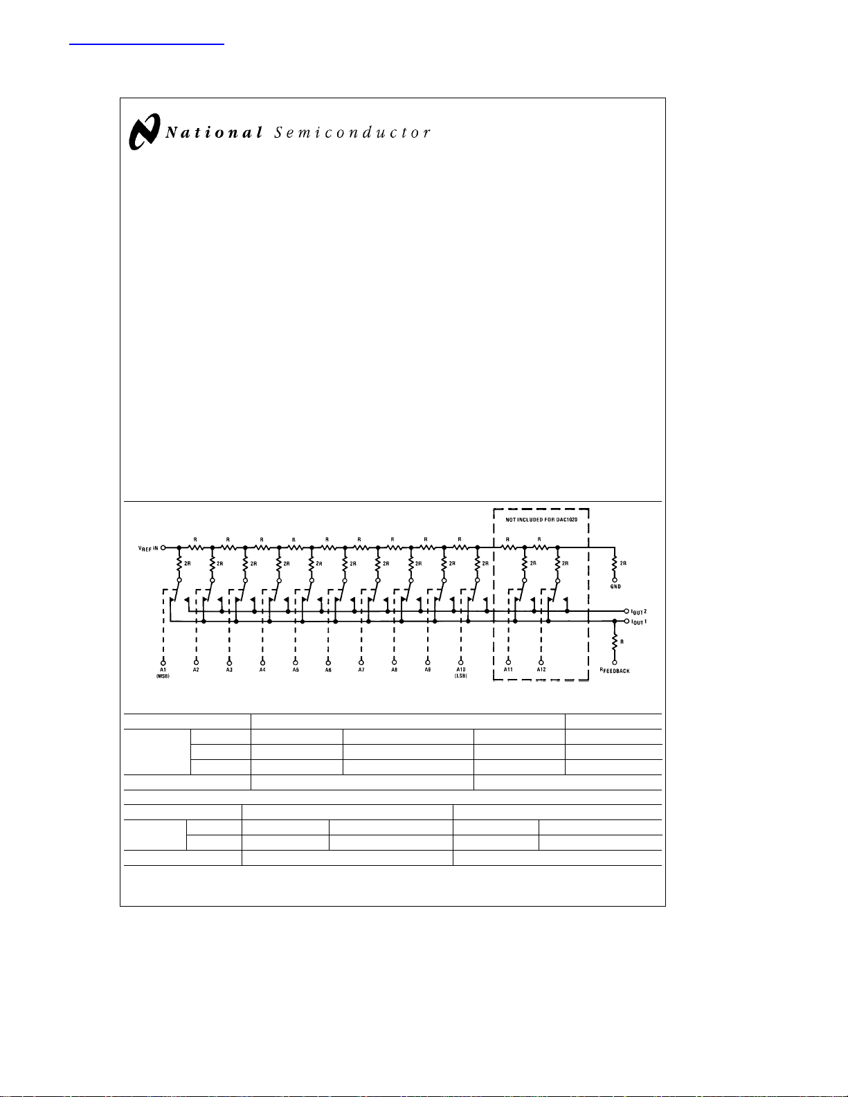
Equivalent Circuit Note. Switches shown in digital high state
Ordering Information
Temperature Range 0§Cto70§C
Non-
Linearity
Package Outline N16A V20A
Temperature Range 0§Cto70§C
Non-
Linearity
Package Outline N18A J18A
Note. Devices may be ordered by either part number.
C
1996 National Semiconductor Corporation RRD-B30M96/Printed in U. S. A.
0.05% DAC1020LCN AD7520LN,AD7530LN DAC1020LCV DAC1020LIV
0.10% DAC1021LCN AD7520KN,AD7530KN
0.20% DAC1022LCN AD7520JN,AD7530JN
0.05% DAC1220LCN AD7521LN,AD7531LN DAC1220LCJ AD7521LD,AD7531LD
0.20% DAC1222LCN AD7521JN,AD7531JN DAC1222LCJ AD7521JD,AD7531JD
TL/H/5689
10-BIT D/A CONVERTERS
12-BIT D/A CONVERTERS
b
40§Ctoa85§C
TL/H/5689– 1
b
40§Cto85§C
http://www.national.com
Page 2
Absolute Maximum Ratings (Note 5)
If Military/Aerospace specified devices are required,
please contact the National Semiconductor Sales
Office/Distributors for availability and specifications.
a
V
to Gnd 17V
V
to Gnd
REF
Digital Input Voltage Range V
DC Voltage at Pin 1 or Pin 2 (Note 3)
Storage Temperature Range
b
b
65§Ctoa150§C
g
a
to Gnd
100 mV to V
25V
a
Operating Ratings
Temperature (T
DAC1020LIV, DAC1220LCJ,
DAC1222LCJ
DAC1020LCN, DAC1020LCV,
DAC1021LCN 0
DAC1022LCN, DAC1220LCN 0
DAC1222LCN 0
)
A
Min Max Units
b
40a85
a
a
a
§
70
§
70
§
70
§
C
C
C
C
Lead Temperature (Soldering, 10 sec.)
Dual-In-Line Package (plastic) 260
Dual-In-Line Package (ceramic) 300
C
§
C
§
ESD Susceptibility (Note 4) 800V
a
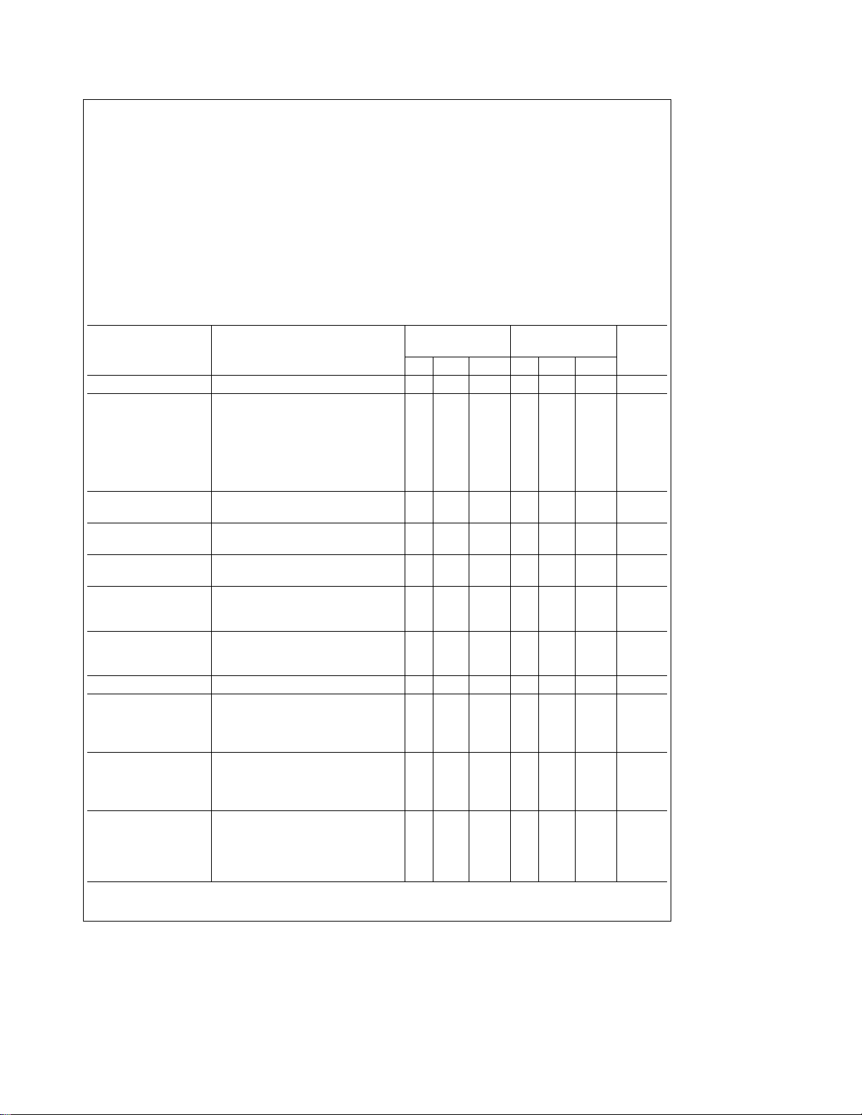
Electrical Characteristics (V
e
15V, V
Parameter Conditions DAC1022 Units
REF
e
10.000V, T
e
25§C unless otherwise specified)
A
DAC1020, DAC1021,
DAC1220, DAC1222
Min Typ Max Min Typ Max
Resolution 10 12 Bits
k
Linearity Error T
k
T
T
MIN
b
10VkV
(Note 1) End Point Adjustment Only
,
A
MAX
k
a
10V,
REF
(See Linearity Error in Definition of Terms)
10-Bit Parts DAC1020, DAC1220 0.05 0.05 % FSR
9-Bit Parts DAC1021 0.10 0.10 % FSR
8-Bit Parts DAC1022, DAC1222 0.20 0.20 % FSR
k
T
A
s
T
A
a
s
a
10V, 0.0002 0.0002 % FS/§C
REF
s
a
10V, 0.3 1.0 0.3 1.0 % FS
REF
k
T
, 0.001 0.001 % FS/§C
MAX
s
T
MAX
s
16V, (Note 2),
Linearity Error Tempco
b
10VsV
(Notes 1 and 2)
Full-Scale Error
b
10VsV
(Notes 1 and 2)
Full-Scale Error Tempco T
Output Leakage Current T
I
OUT 1
I
OUT 2
MIN
(Note 2)
MIN
All Digital Inputs Low 200 200 nA
All Digital Inputs High 200 200 nA
Power Supply Sensitivity All Digital Inputs High, 0.005 0.005 % FS/V
14VsV
(Figure 2)
V
Input Resistance 10 15 20 10 15 20 kX
REF
Full-Scale Current Settling R
Time FS
e
100X from 0 to 99. 95%
L
All Digital Inputs Switched 500 500 ns
Simultaneously
V
Feedthrough All Digital Inputs Low, 10 10 mVp-p
REF
e
V
20 Vp-p@100 kHz
REF
J Package (Note 4) 6 9 6 9 mVp-p
N Package 2 5 2 5 mVp-p
Output Capacitance
I
OUT 1
I
OUT 2
All Digital Inputs Low 40 40 pF
All Digital Inputs High 200 200 pF
All Digital Inputs Low 200 200 pF
All Digital Inputs High 40 40 pF
http://www.national.com 2
Page 3
a
Electrical Characteristics (V
e
15V, V
Parameter Conditions DAC1022 Units
e
10.000V, T
REF
DAC1020, DAC1021,
e
25§C unless otherwise specified) (Continued)
A
DAC1220, DAC1222
Min Typ Max Min Typ Max
Digital Input
Low Threshold T
High Threshold T
Digital Input Current T
(Figure 1)
k
k
T
MIN
MIN
MIN
Digital Input High 1 100 1 100 mA
Digital Input Low
T
A
MAX
k
k
T
T
A
MAX
s
s
T
T
A
MAX
2.4 2.4 V
b
50
0.8 0.8 V
b
200
b
b
50
200 mA
Supply Current All Digital Inputs High 0.2 1.6 0.2 1.6 mA
All Digital Inputs Low 0.6 2 0.6 2 mA
Operating Power Supply
(Figures 1 and 2)
5 15 5 15 V
Range
e
Note 1: V
linearity error. For instance, if the linearity error at 25
however, that the linearity error is specified over the device full temperature range which is a more stringent specification since
temperature coefficient.
Note 2: Using internal feedback resistor as shown in
Note 3: Both I
0.005% linearity error will be introduced.
Note 4: Human body model, 100 pF discharged through a 1.5 kX resistor.
Note 5: Absolute Maximum Ratings indicate limits beyond which damage to the device may occur. DC and AC electrical specifications do not apply when operating
the device beyond its specified operating conditions.
Note 6: The maximum power dissipation must be derated at elevated temperatures and is dictated by T
allowable power dissipation at any temperature is P
device, T
120
§
g
10V and V
REF
and I
OUT 1
e
125§C, and the typical junction-to-ambient thermal resistance of the J18 package when board mounted is 85§C/W. For the N18 package, iJAis
JMAX
C/W, for the N16 this number is 125§C/W, and for the V20 this number is 95§C/W.
e
g
1V. A linearity error temperature coefficient of 0.0002% FS for a 45§C rise only guarantees 0.009% maximum change in
REF
must go to ground or the virtual ground of an operational amplifier. If V
OUT 2
C is 0.045% FS it could increase to 0.054% at 70§C and the DAC will be no longer a 10-bit part. Note,
§
Figure 3
e
D
.
b
(T
TA)/iJAor the number given in the Absolute Maximum Ratings, whichever is lower. For this
JMAX
e
10V, every millivolt offset between I
REF
, iJA, and the ambient temepature, TA. The maximum
JMAX
it includes
the linearity error
or I
OUT 1
OUT 2
,
Typical Performance Characteristics
FIGURE 1. Digital Input Threshold vs
Ambient Temperature
FIGURE 2. Gain Error Variation vs V
http://www.national.com3
a
TL/H/5689– 2
Page 4
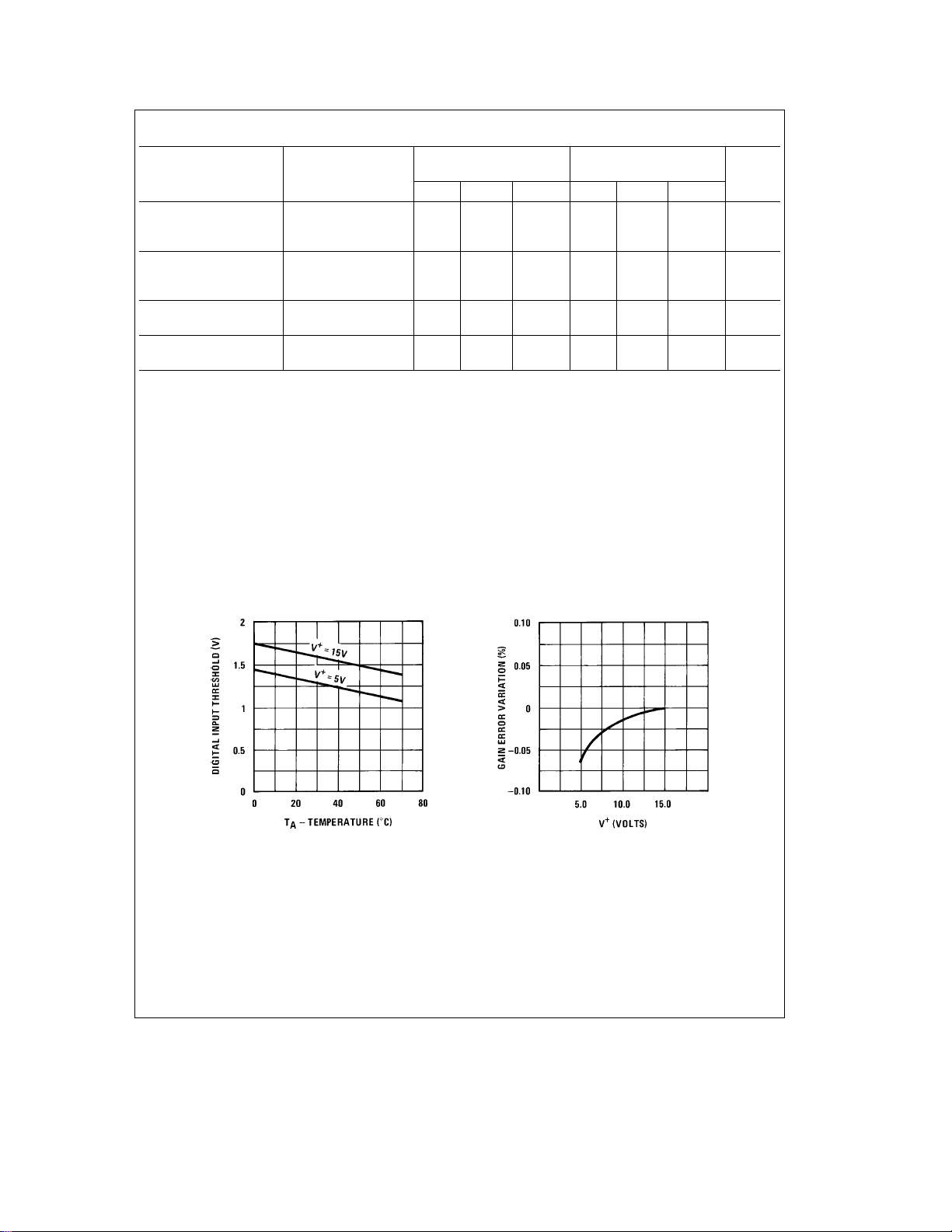
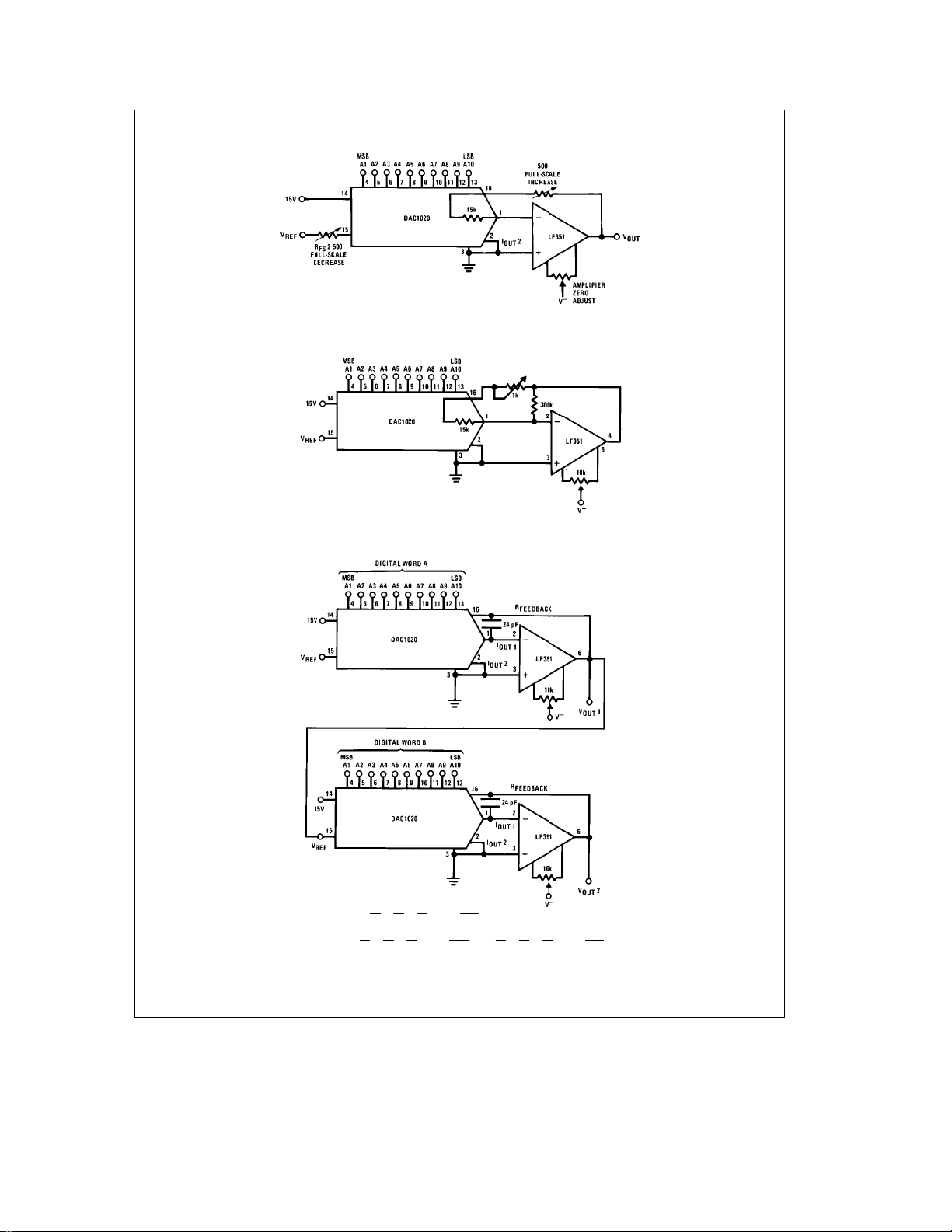
Typical Applications
The following applications are also valid for 12-bit systems
using the DAC1220 and 2 additional digital inputs.
Operational Amplifier Bias Current (
The op amp bias current, Ib, flows through the 15k internal
feedback resistor. BI-FET op amps have low I
fore, the 15k
c
Iberror they introduce is negligible; they are
strongly recommended for the DAC1020 applications.
V
Considerations
OS
The output impedance, R
the digital input code which causes a modulation of the op-
OUT
erational amplifier output offset. It is therefore recommended to adjust the op amp V
digital inputs are high; R
is high, and R
OUT
OS.ROUT
OUT
approaches infinity if all inputs are low.
SELECTING AND COMPENSATING THE OPERATIONAL AMPLIFIER
Op Amp Family C
LF357 10 pF 2.4k 25k V
LF356 22 pF
LF351 24 pF
LM741 0
Figure 3
)
and, there-
b
, of the DAC is modulated by
isE15k if more than 4
isE45k if a single digital input
F
R
i
%
%
%
Operational Amplifier V
OS
Adjust (
Figure 3
Connect all digital inputs, A1 –A10, to ground and adjust the
potentiometer to bring the op amp V
mV from ground potential. If V
V
adjustment is required. It is helpful to increase the reso-
OS
lution of the V
resistor between the inverting input of the op amp to
ground. After V
Full-Scale Adjust (
adjust procedure by connectinga1kX
OS
has been adjusted, remove the 1 kX.
OS
Figure 4
)
OUT
is less than 10V, a finer
REF
Switch high all the digital inputs, A1 –A10, and measure the
op amp output voltage. Use a 500X potentiometer, as
shown, to bring
1023/1024.
PV
25k V
10k V
10k V
W
a
a
b
b
V
to a voltage equal to V
ll
ll
OUT
Circuit Settling Circuit Small
Time, t
s
1.5 ms1M
3 ms 0.5M
4 ms 0.5M
40 ms 200 kHz
)
pin to withing1
REF
Signal BW
c
V
OUT
b
10VsV
s
0
V
where A
eb
OUT
A1
V
REF
2
#
s
10V
REF
1023
s
b
V
1024
e
1 if the ANdigital input is high
N
e
A
0 if the ANdigital input is low
N
FIGURE 3. Basic Connection: Unipolar or 2-Quadrant Multiplying
Configuration (Digital Attenuator)
http://www.national.com 4
A2
A3
a
a
4
REF
A10
a
###
8
1024
J
TL/H/5689– 3
Page 5
Typical Applications (Continued)
FIGURE 5. Alternate Full-Scale Adjust: (Allows Increasing or Decreasing the Gain)
FIGURE 4. Full-Scale Adjust
A1
A2
A3
V
OUT 1
V
OUT2
where V
eb
V
REF
#
A1
e
V
REF
2
#
can be an AC signal
REF
a
a
2
4
A2
A3
a
a
4
8
A10
a
###
8
1024
A10
a
###
1024
Jc#
FIGURE 6. Precision Analog-to-Digital Multiplier
J
B1
B2
B3
a
a
2
4
B10
a
###
8
1024
J
TL/H/5689– 4
http://www.national.com5
Page 6

Typical Applications (Continued)
A1
eb
V
V
OUT
REF
where: ANea1ifANinput is high
eb
AN
A2
a
2
4
#
1ifANinput is low
A10
a
a
1024
b
###
FIGURE 7. Bipolar 4-Quadrant Multiplying Configuration
Operational Amplifiers V
OS
Adjust (
a) Switch all the digital inputs high; adjust the V
ometer of op amp B to bring its output to a value equal
b
to
(V
/1024) (V).
REF
b) Switch the MSB high and the remaining digital inputs
low. Adjust the V
its output value to withina1mVfrom ground potential.
For V
mentioned in the previous application.
REF
k
potentiometer of op amp A, to bring
OS
10V, a finer adjust is necessary, as already
1
1024
J
Figure 7
TL/H/5689– 5
)
potenti-
OS
COMPLEMENTARY OFFSET BINARY
(BIPOLAR) OPERATION
DIGITAL INPUT V
0000000000
0000000001 V
0111111111 V
1000000000 0
1000000001
1111111111
REF
b
b
V
REF
V
REF
REF
OUT
a
V
REF
c
1022/1024
c
2/1024
c
2/1024
(1022/1024)
Note that:
V
a
I
#
#
I
OUT 1
OUT 2
By doubling the output range we get half the
e
REF
R
LADDER
1023
c
1024
#
J
resolution
The 10M resistor, adds a 1 LSB ‘‘thump’’, to
#
allow full offset binary operation where the output reaches zero for the half-scale code. If
symmetrical output excursions are required,
omit the 10M resistor.
Gain Adjust (Full-Scale Adjust)
Assuming that the external 10k resistors are matched to
better than 0.1%, the gain adjust of the circuit is the same
with the one previously discussed.
TRUE OFFSET BINARY OPERATION
DIGITAL INPUT V
1111111111V
1000000000 0
0000000000
e
t
1.8 ms
s
use LM336 for a voltage reference
REF
OUT
c
1022/1024
b
V
REF
FIGURE 8. Bipolar Configuration with a Single Op Amp
http://www.national.com 6
R4e(2A
#
R3
Example: V
#
Then R4
R3
b
A
R2
R1
V
2V, V
V
e
,
b
b
A
1
V
V
OUT(PEAK)
b
e
OUT
V
REF
(swing)
,Re20k
j
g
10V: A
b
b
1) R,
V
a
R1llR2eR; A
e
REF
e
9R, R1e0.8 R2. If R1e0.2R then R2e0.25R,
e
0.64R
FIGURE 9. Bipolar Configuration with
Increased Output Swing
V
b
e
5V
TL/H/5689– 6
Page 7

Typical Applications (Continued)
e
V
OUT
A1
A2
a
2
#
where: V
By connecting the DAC in the feedback loop of an opera-
#
tional amplifier a linear digitally control gain block can be
realized
Note that with all digital inputs low, the gain of the amplifier
#
is infinity, that is, the op amp will saturate. In other words, we
cannot divide the V
FIGURE 10. Analog-to-Digital Divider (or Digitally Gain Controlled Amplifier)
can be an AC signal
REF
b
V
REF
A3
a
4
A10
a
...
8
1024
J
by zero!
REF
A1
A2
a
2
e
V
V
OUT
REF
4
A1
A2
a
2
4
%
FIGURE 11. Digitally controlled Amplifier-Attenuator
A10
a
a
...
1024
or V
OUT
A10
a
a
...
1024
–
where: 0sNs1023
e
N
0 for A
e
N
1 for A10e1, A1– A9e0
.
.
.
e
N
1023 for A
1023bN
e
V
REF
#
e
all zeros
N
e
N
N
all 1’s
TL/H/5689– 7
J
http://www.national.com7
Page 8

Typical Applications (Continued)
f
CLK
Output frequency
#
Output voltage rangee0Vb10V peak
#
THDk0.2%
#
Excellent amplitude and frequency stability with temperature
#
Low pass filter shown has a 1 kHz corner (for output frequencies below 10 Hz,
#
filter corner should be reduced)
Any periodic function can be implemented by modifying the contents of the look
#
up table ROM
No start up problems
#
FIGURE 12. Precision Low Frequency Sine Wave Oscillator Using Sine Look-Up ROM
http://www.national.com 8
e
512
;f
MAX
j
TL/H/5689– 8
2 kHz
Page 9

Typical Applications (Continued)
MM74C00 Ð NAND gates
MM74C32 Ð OR gates
MM74C74 Ð D flip-flop
MM74C193 Ð Binary up/
down counters
Binary up/down counter digitally ‘‘ramps’’ the DAC
#
output
Can stop counting at any desired 10-bit input code
#
Senses up or down count overflow and automatically
#
reverses direction of count
FIGURE 13. A Useful Digital Input Code Generator for DAC Attenuator or Amplifier Circuits
TL/H/5689– 9
http://www.national.com9
Page 10

Definition of Terms
Resolution: Resolution is defined as the reciprocal of the
number of discrete steps in the D/A output. It is directly
related to the number of switches or bits within the D/A. For
example, the DAC1020 has 2
DAC1220 has 2
12
or 4096 steps. Therefore, the DAC1020
has 10-bit resolution, while the DAC1220 has 12-bit resolution.
Linearity Error: Linearity error is the maximum deviation
from
a straight line passing through the endpoints of the
D/A transfer characteristic.
for zero (see V
scale. Linearity error is a design parameter intrinsic to the
adjust in typical applications) and full-
OS
device and cannot be externally adjusted.
10
or 1024 steps while the
It is measured after calibrating
Power Supply Sensitivity: Power supply sensitivity is a
measure of the effect of power supply changes on the D/A
full-scale output.
Settling Time: Full-scale settling time requires a zero to fullscale or full-scale to zero output change. Settling time is the
time required from a code transition until the D/A output
reaches within
g
(/2 LSB of final output value.
Full-Scale Error: Full-scale error is a measure of the output
error between an ideal D/A and the actual device output.
Ideally, for the DAC1020 full-scale is V
e
V
10V and unipolar operation, V
REF
e
10.0000VÐ9.8 mVe9.9902V. Full-scale error is ad-
LE
justable to zero as shown in
Figure 5
b
1 LSB. For
REF
FULL-SCA-
.
ab1b2
TL/H/5689– 10
(a) End point test after zero and full-scale adjust.
The DAC has 1 LSB linearity error.
Note. (a), (b1) and (b2) above illustrate the difference between ‘‘end point’’ National’s linearity test (a) and ‘‘best straight line’’ test. Note that both devices in (a) and
(b2) meet the
g
(/2 LSB linearity error specification but the end point test is a more ‘‘real life’’ way of characterizing the DAC.
(b) By shifting the full-scale calibration on of the DAC of
Figure (b1)
test and meet the
we could pass the ‘‘best straight line’’ (b2)
g
(/2 linearity error specification.
Connection Diagrams
DAC102X
Dual-In-Line Package
TL/H/5689– 13
DAC1020
PLCC Package
DAC122X
Dual-In-Line Package
TL/H/5689– 12
TL/H/5689– 11
http://www.national.com 10
Page 11

http://www.national.com11
Page 12

Physical Dimensions inches (millimeters) unless otherwise noted
Cavity Dual-In-Line Package (J)
Order Number DAC1220LCJ or DAC1222LCJ
NS Package Number J18A
Order Number DAC1020LCN, DAC1021LCN or DAC1022LCN
http://www.national.com 12
Molded Dual-In-Line Package (N)
NS Package Number N16A
Page 13

Physical Dimensions inches (millimeters) unless otherwise noted (Continued)
Order Number DAC1220LCN, DAC1221LCN or DAC1222LCN
Molded Dual-In-Line Package (N)
NS Package Number N18A
http://www.national.com13
Page 14

Physical Dimensions inches (millimeters) unless otherwise noted (Continued)
Molded Plastic Leaded Chip Carrier (V)
Order Number DAC1020LCV or DAC1020LIV
NS Package Number V20A
DAC1220/DAC1222 12-Bit Binary Multiplying D/A Converter
LIFE SUPPORT POLICY
DAC1020/DAC1021/DAC1022 10-Bit Binary Multiplying D/A Converter
NATIONAL’S PRODUCTS ARE NOT AUTHORIZED FOR USE AS CRITICAL COMPONENTS IN LIFE SUPPORT
DEVICES OR SYSTEMS WITHOUT THE EXPRESS WRITTEN APPROVAL OF THE PRESIDENT OF NATIONAL
SEMICONDUCTOR CORPORATION. As used herein:
1. Life support devices or systems are devices or 2. A critical component is any component of a life
systems which, (a) are intended for surgical implant support device or system whose failure to perform can
into the body, or (b) support or sustain life, and whose be reasonably expected to cause the failure of the life
failure to perform, when properly used in accordance support device or system, or to affect its safety or
with instructions for use provided in the labeling, can effectiveness.
be reasonably expected to result in a significant injury
to the user.
National Semiconductor National Semiconductor National Semiconductor National Semiconductor
Corporation Europe Hong Kong Ltd. Japan Ltd.
1111 West Bardin Road Fax:
Arlington, TX 76017 Email: europe.support@nsc.com Ocean Centre, 5 Canton Rd. Fax: 81-043-299-2408
Tel: 1(800) 272-9959 Deutsch Tel:
Fax: 1(800) 737-7018 English Tel:
http://www.national.com
National does not assume any responsibility for use of any circuitry described, no circuit patent licenses are implied and National reserves the right at any time without notice to change said circuitry and specifications.
Fran3ais Tel:
Italiano Tel:a49 (0) 180-534 16 80 Fax: (852) 2736-9960
a
49 (0) 180-530 85 86 13th Floor, Straight Block, Tel: 81-043-299-2308
a
49 (0) 180-530 85 85 Tsimshatsui, Kowloon
a
49 (0) 180-532 78 32 Hong Kong
a
49 (0) 180-532 93 58 Tel: (852) 2737-1600
 Loading...