

Page 1
10-Bit High Speed Multiplying D/A Converter
a
(Universal Digital Logic Interface)
FEATURES
Fast Settling: 85 ns
Low Full-Scale Drift: 10 ppm/8C
Nonlinearity to 0.05% Max Over Temperature Range
Complementary Current Outputs: 0 mA to 4 mA␣
Wide Range Multiplying Capability: 1 MHz Bandwidth
Wide Power Supply Range: +5, –7.5 Min to 618 V Max
Direct Interface to TTL, CMOS, ECL, PMOS, NMOS
Availability in Die Form␣
GENERAL DESCRIPTION
The DAC10 series of 10-bit monolithic multiplying digital-toanalog converters provide high speed performance and full-scale
accuracy.
Advanced circuit design achieves 85 ns settling times with very
low “glitch” energy and low power consumption. Direct interface to all popular logic families with full noise immunity is
provided by the high swing, adjustable threshold logic inputs.
DAC10*
All DAC10 series models guarantee full 10-bit monotonicity,
and nonlinearities as tight as +0.05% over the entire operating
temperature range are available. Device performance is essentially unchanged over the ± 18 V power supply range, with
85 mW power consumption attainable at lower supplies.
A highly stable, unique trim method is used, which selectively
shorts Zener diodes, to provide 1/2 LSB full-scale accuracy
without the need for laser trimming.
Single-chip reliability, coupled with low cost and outstanding
flexibility, make the DAC10 device an ideal building block for
A/D converters, Data Acquisition systems, CRT displays, programmable test equipment and other applications where low
power consumption, input/output versatility and long-term
stability are required.
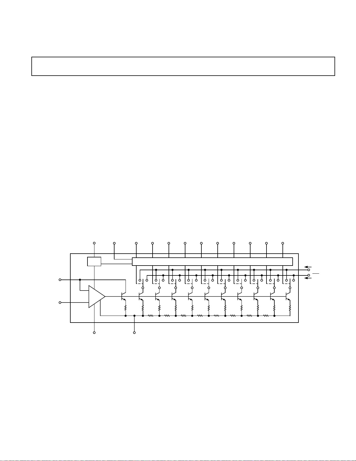
SIMPLIFIED SCHEMATIC
V+
16
(+)
V
REF
V
REF
17
(–)
COMP V–
V
LC
15 1 5 6 7 8 9 10 11 12 13 14
BIAS NETWORK
CURRENT SWITCHES
REFERENCE
AMPLIFIER
18 3
MSB
B
B
B
B
B
B
B
1
2
3
4
5
6
B
7
8
LSB
B
B
9
10
4
I
OUT
I
OUT
2
*Protected by Patent Nos. 4,055,770, 4,056,740 and 4,092,639.
REV. D
Information furnished by Analog Devices is believed to be accurate and
reliable. However, no responsibility is assumed by Analog Devices for its
use, nor for any infringements of patents or other rights of third parties
which may result from its use. No license is granted by implication or
otherwise under any patent or patent rights of Analog Devices.
One Technology Way, P.O. Box 9106, Norwood, MA 02062-9106, U.S.A.
Tel: 781/329-4700 World Wide Web Site: http://www.analog.com
Fax: 781/326-8703 © Analog Devices, Inc., 1998
Page 2
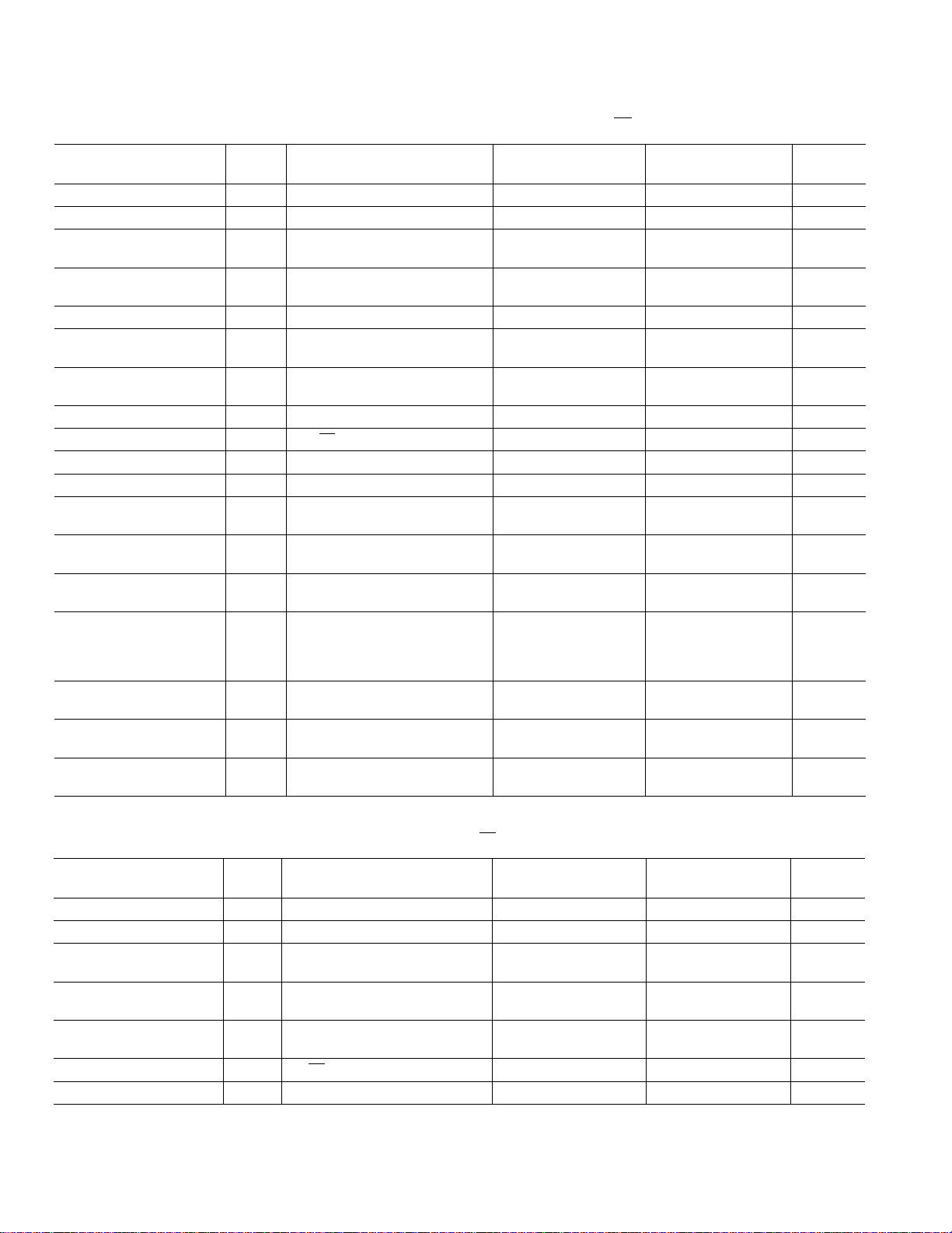
DAC10–SPECIFICATIONS
(@ VS = 615 V; I
ELECTRICAL CHARACTERISTICS
Parameter Symbol Conditions Min Typ Max Min Typ Max Units
MONOTONICITY 10 10 Bits
NONLINEARITY NL 0.3 0.5 0.6 1 LSB
DIFFERENTIAL
NONLINEARITY DNL 0.3 1 0.7 LSB
SETTLING TIME t
OUTPUT CAPACITANCE C
PROPAGATION DELAY t
t
S
O
PLH
PHL
OUTPUT VOLTAGE Full-Scale Current Change –5.5 –5.5 V
COMPLIANCE V
OC
GAIN TEMPCO TCI
FULL-SCALE SYMMETRY I
ZERO-SCALE CURRENT I
FULL-SCALE CURRENT I
FSS
ZS
FR
REFERENCE INPUT
SLEW RATE DI/dt 6 6 mA/µs
REFERENCE BIAS
CURRENT I
B
POWER SUPPLY PPS/
SENSITIVITY PPS/FS– –18 V ≤ V– ≤ –10 V 0.0012 0.01 0.0012 0.01 %∆IFS/%∆V
POWER SUPPLY CURRENT I+ V
I– –9 –15 –9 –15 mA
I+ V
I– –5.9 –9 –5.9 –9 mA
POWER DISSIPATION P
LOGIC INPUT LEVELS V
LOGIC INPUT CURRENTS I
D
P
D
IL
V
IH
IL
I
IH
All Bits Switched ON or OFF
Settle to 0.05% of FS (See Note) 85 135 85 150 ns
All Bits Switched RL = 5 kΩ 50 50 ns
<1 LSB +10 +10 V
(See Note) ±10 ±25 ±10 ±50 ppm/°C
FS
IFR–I
(See Note) 3.960 3.996 4.032 3.920 3.996 4.072 mA
+ 4.5 V ≤ V+ ≤ –18 V 0.001 0.01 0.001 0.01 %∆IFS/%∆V
FS
S
S
VS = ±15 V; I
VS = +5 V; –7.5 V; I
VLC = 0 0.8 0.8 V
VLC = 0 2 2 V
VLC = 0; VIN = 0.8 V –10 –5 –10 –5 µA
VIN = 2.0 V 0.001 10 0.001 10 µA
Output characteristics apply to both I
RL = 0 kΩ 50 50 ns
FR
= ±15 V; I
= +5 V; –7.5 V; I
= 2 mA 2.3 4 2.3 4 mA
REF
REF
= 2 mA 231 285 231 285 mW
REF
REF
= 2 mA; 08C ≤ TA ≤ +708C for DAC10F and G, unless otherwise noted.
REF
OUT
and I
OUT
.)
DAC10F DAC10G
18 18 pF
0.1 4 0.1 4 µA
0.01 0.5 0.01 0.5 µA
–1 –3 –1 –3 µA
= 1 mA 1.8 4 1.8 4 mA
= 1 mA 85 88 85 88 mW
ELECTRICAL CHARACTERISTICS
(@ VS = 615 V; I
apply to both I
= 2 mA; TA = +258C, unless otherwise noted. Output characteristics
REF
OUT
and I
OUT
.)
DAC10F DAC10G
Parameter Symbol Conditions Min Typ Max Min Typ Max Units
MONOTONICITY 10 10 Bits
NONLINEARITY NL 0.3 0.5 0.6 1 LSB
DIFFERENTIAL
NONLINEARITY DNL 0.3 1 0.7 LSB
OUTPUT VOLTAGE
COMPLIANCE V
FULL-SCALE CURRENT I
OC
FS
Full-Scale Current Change, <1 LSB –5 –6/+18 +10 –5 –6/+15 +10 V
V
= 10.000 V,
REF
R14 = R15 = 5.000 kΩ 3.978 3.996 4.014 3.956 3.996 4.036 mA
FULL-SCALE SYMMETRY I
ZERO-SCALE CURRENT I
NOTE: Guaranteed by design.
FSS
ZS
IFR–I
FR
0.1 4 0.1 0.4 µA
0.01 0.5 0.01 0.5 µA
–2–
REV. D
Page 3
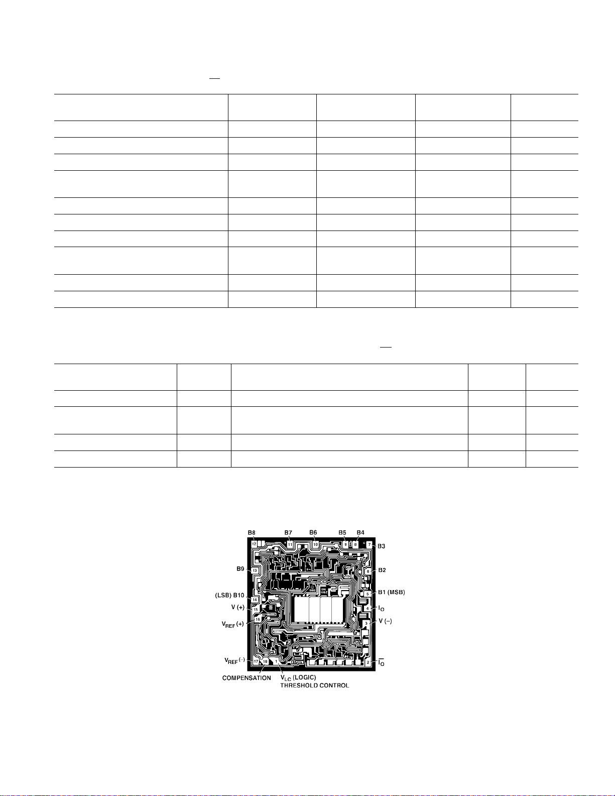
DAC10
WAFER TEST LIMITS
(@ VS = 615 V, I
I
and I
OUT
OUT
= 2 mA, TA = +258C, unless otherwise noted. Output characteristics refer to both
REF
).
DAC10N
Parameter Symbol Conditions Limit Units
RESOLUTION 10 Bits min
MONOTONICITY 10 Bits min
NONLINEARITY NL ±0.5 LSB max
OUTPUT VOLTAGE COMPLIANCE V
OC
True 1 LSB +10 V max
–5 V min
OUTPUT CURRENT RANGE I
ZERO-SCALE CURRENT I
LOGIC INPUT “1” V
LOGIC INPUT “0” V
ZS
IH
IL
±3.996 mA ±18 µA max
FS
All Bits OFF 0.5 µA max
IIN = 100 nA 2 V min
VLC @ Ground 0.8 V max
I
= –100 µA
IN
POSITIVE SUPPLY CURRENT I+ V+ = 15 V 4 mA max
NEGATIVE SUPPLY CURRENT I– V+ = –15 V –15 mA max
NOTE: Electrical tests are performed at wafer probe to the limits shown. Due to variations in assembly methods and normal yield loss, yield after packaging is not
guaranteed for standard produce dice.
TYPICAL ELECTRICAL CHARACTERISTICS
(@ VS = 615 V, I
refer to both I
= 2 mA, unless otherwise noted. Output characteristics
REF
OUT
and I
OUT
).
DAC10F
Parameter Symbol Conditions Typ Units
SETTLING TIME t
S
To ±1/2 LSB When Output Is Switched from 0 to FS 85 ns
GAIN TEMPERATURE
COEFFICIENT (TC) V
Tempco Excluded ±10 ppm FS/°C
REF
OUTPUT CAPACITANCE 18 pF
OUTPUT RESISTANCE 10 MΩ
DICE CHARACTERISTICS
DIE SIZE 0.091 3 0.087 inch, 7,917 sq. mils
(2.311 3 2.210 mm, 5.107 sq. mm)
–3–REV. D
Page 4
DAC10
ABSOLUTE MAXIMUM RATINGS
1
Operating Temperature
DAC10FX, GX, GS, GP . . . . . . . . . . . . . . . . 0°C to +70°C
Junction Temperature (T
) . . . . . . . . . . . . . –65°C to +150°C
J
Storage Temperature . . . . . . . . . . . . . . . . . . –65°C to +150°C
Lead Temperature (Soldering, 60 sec) . . . . . . . . . . . +300°C
V+ Supply to V– Supply . . . . . . . . . . . . . . . . . . . . . . . . . 36 V
Logic Inputs . . . . . . . . . . . . . . . . . . . . . . V– to V– plus 36 V
V
␣ . . . . . . . . . . . . . . . . . . . . . . . . . . . . . . . . . . . . . V– to V+
LC
Analog Current Outputs . . . . . . . . . . . . . . . . +18 V to –18 V
Reference Inputs (V
Reference Input Differential Voltage (V
Reference Input Current (I
Package Type u
to V17) . . . . . . . . . . . . . . . . . V– to V+
16
) . . . . . . . . . . . . . . . . . . 2.5 mA
16
to V
16
2
JA
) . . . . ±18 V
17
u
JC
Units
18-Lead Hermetic DIP (X) 48 15 °C/W
18-Lead SOIC (S) 89 28 °C/W
18-Lead Plastic DIP (P) 74 33 °C/W
NOTES
1
Absolute maximum ratings apply to both DICE and packaged parts, unless
otherwise noted.
2
θJA is specified for worst case mounting conditions, i.e., θJA is specified for device
in socket for Cerdip packages.
ORDERING GUIDE
INL Temperature Package Package
Model (LSB) Range Description Options
DAC10FX 0.5 0°C to +70°C Cerdip Q-18
DAC10GX 1 0°C to +70°C Cerdip Q-18
DAC10GS 1 0°C to +70°C SOIC R-18
DAC10GP 1 0°C to +70°C Plastic DIP N-18
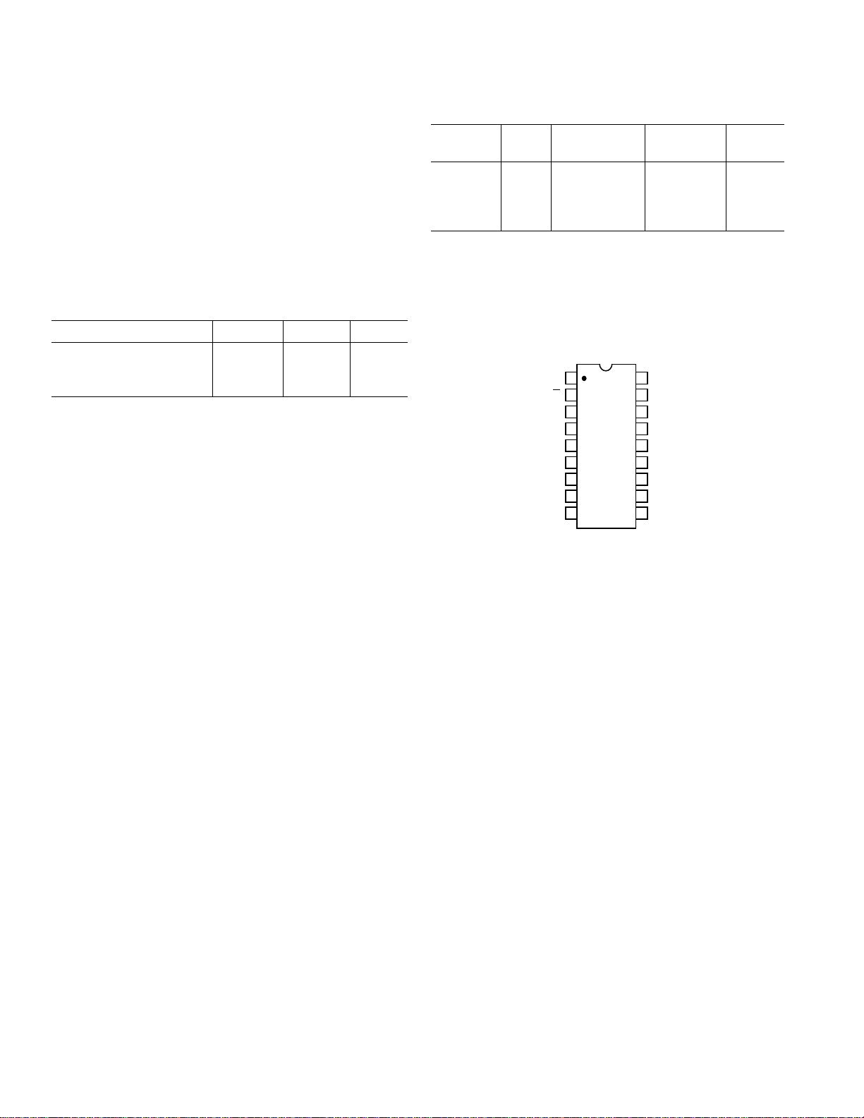
PIN CONNECTIONS
18-Lead Hermetic DIP
18-Lead Plastic DIP
18-Lead SOIC
V
V–
(MSB) B1
B2
B3
B4
B5
LC
I
O
I
O
1
2
3
4
DAC10
5
TOP VIEW
(Not to Scale)
6
7
8
9
18
COMP
17
V
16
V
15
V+
14
B10 (LSB)
13
B9
12
B8
11
B7
10
B6
REF
REF
(–)
(+)
–4–
REV. D
Page 5
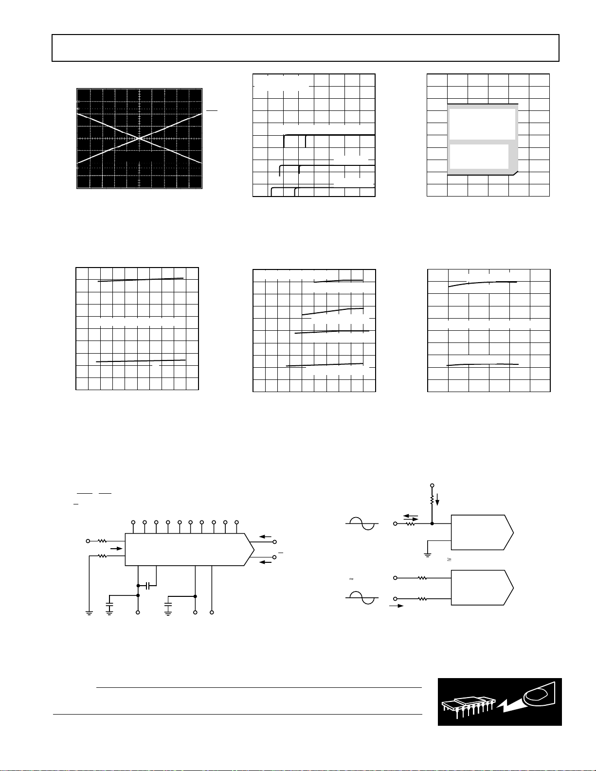
Typical Performance Characteristics–DAC10
DAC10
DAC10
16
17
16
17
V
IN
V
IN
I
IN
R
REF
R17
(OPTIONAL)
R
IN
I
REF
+V
REF
R
REF
R
REF
R17
+V
REF
I
REF
PEAK NEGATIVE SWING OF I
IN
+V
REF
MUST BE ABOVE PEAK POSITIVE SWING OF V
IN
HIGH INPUT
IMPEDANCE
0mA
1.0mA
I
= 2mA
2.0mA
(0000000000) (11111111111)
REF
Figure 1. True and Complementary
Output Operations
10
9
8
7
6
ALL BITS "HIGH" OR "LOW"
5
4
3
2
POWER SUPPLY CURRENT – mA
1
0
4681012141618
02 20
V+, POSITIVE POWER SUPPLY – V
I–
I+
DC
Figure 4. Power Supply Current
vs. V+
8.0
TA = T
TO T
MIN
7.2
ALL BITS ON
6.4
I
OUT
I
OUT
5.6
4.8
4.0
3.2
2.4
OUTPUT CURRENT – mA
1.6
0.8
0
–14 –10 18–6 –2 2 6 10 14
MAX
V– = –15V, V– = –10V
OUTPUT VOLTAGE – Volts
Figure 2. Output Current vs. Output
Voltage (Output Voltage Compliance)
10
BITS MAY BE HIGH OR LOW
9
8
7
6
5
4
3
2
POWER SUPPLY CURRENT – mA
1
0
0 –20
–4 –8 –12 –16
V–, NEGATIVE POWER SUPPLY – V
I – WITH I
I – WITH I
I – WITH I
I – WITH I
REF
REF
Figure 5. Power Supply Current
vs. V–
I
I
I
REF
REF
REF
REF
REF
= 2mA
= 1mA
= 0.2mA
= 2mA
= 1mA
= 0.2mA
= 0.2mA
DC
+28
+24
+20
+16
+12
+8
+4
0
–4
OUTPUT VOLTAGE – Volts
–8
–12
SHADED AREA INDICATES
PERMISSABLE OUTPUT
VOLTAGE RANGE
FOR V– = –15V
# 2.0mA
I
REF
FOR OTHER V– OR I
SEE OUTPUT CURRENT
vs. OUTPUT VOLTAGE
CURVE
0
–50
+50 +100 +150
TEMPERATURE – 8C
REF
Figure 3. Output Voltage Compliance
vs. Temperature
10
9
8
7
6
5
4
3
2
POWER SUPPLY CURRENT – mA
1
0
V– = –15V
I
= 2.0mA
REF
ALL BITS MAY BE "HIGH" OR "LOW"
V+ = +15V
0 +50 +100 +150
–50
TEMPERATURE – 8C
I–
I+
Figure 6. Power Supply Current vs.
Temperature
BASIC CONNECTIONS
+V
1023
REF
IFR =
R
REF
+ IO = IFR FOR ALL
I
O
LOGIC STATES
+V
REF
CAUTION
ESD (electrostatic discharge) sensitive device. Electrostatic charges as high as 4000 V readily
accumulate on the human body and test equipment and can discharge without detection.
REV. D
3
3
2
1024
R
REF
(R16)
I
REF
R17
Figure 7. Basic Positive Reference Operation
MSB
B
B
1
5 6
16
17
0.1mF
V–
B
2B3
7 8
318
C
C
4
DAC10
COMP
0.01mF
LSB
B
B
B
B
B
5
6
7
9
10
11
15
V+
B
8
9
10
12
13
14
1
FOR FIXED REFERENCE,
TTL OPERATION,
TYPICAL VALUES ARE:
= +10.000V
V
REF
R
= 5.000kV
REF
R15 = R
V
CC = 0.01mF
LC
V
= 0V (GROUND)
LC
4
2
REF
I
O
I
O
Figure 8. Accommodating Bipolar References
WARNING!
ESD SENSITIVE DEVICE
–5–
Page 6
DAC10
LOW T.C.
V
REF
R
REF
16
DAC10
17
NOTE: R
CURRENT CANCELLATION
SETS IFS; R17 IS FOR BIAS
REF
REF
R17
–V
REF
3
2
R
REF
–V
I
FS
4
I
O
2
I
O
+10V
10kV
POT
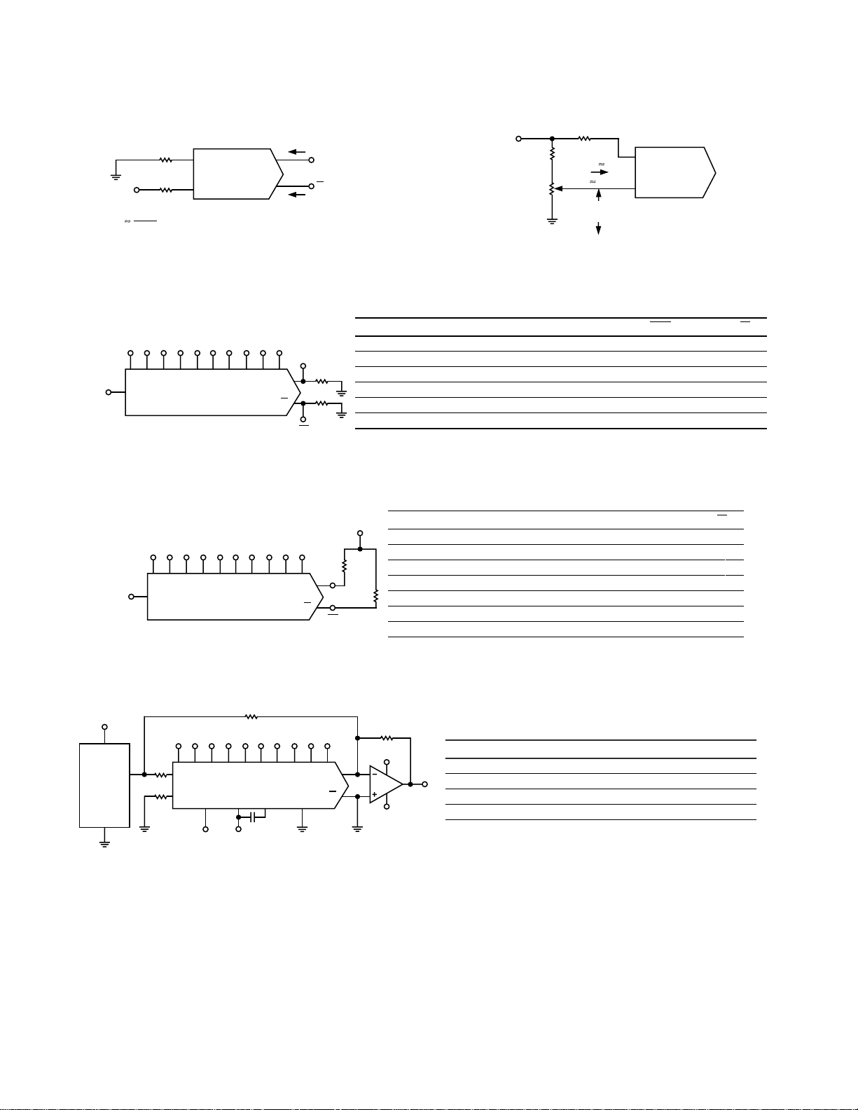
Figure 9. Basic Negative Reference Operation Figure 10. Recommended Full-Scale Adjustment Circuit
4.5kV
39kV
I
(+) 2mA
REF
1V
APPROXIMATELY
5kV
16
DAC10
17
I
REF
2.000mA
MSB
B1B2B3B4B5B6B7B8B9B
=
16
DAC10
MSB
B1B2B3B4B5B6B7B8B9B
=
I
2.000mA
REF01
REF (+)
+15V
V
IN
16
MSB
2
V
O
B1B2B3B4B5B6B7B8B9B
5.000
kV
6
5kV
GND
4
V+
DAC10
5kV
DAC10
V–
LSB
10
E
O
1.25kV
4
I
O
1.25kV
I
O
2
E
O
FULL RANGE
HALF-SCALE +LSB
HALF-SCALE
HALF-SCALE –LSB
HALF-SCALE +LSB
ZERO SCALE +LSB
B1B2B3B4B5B6B7B8B9B
1111111 111
1000000 010
1000000 000
0111111 111
0000000 010
0000000 000
Figure 11. Basic Unipolar Negative Operation
LSB
10
I
O
I
O
+5V
POSITIVE FULL RANGE
POSITIVE FULL RANGE –LSB
2.5kV
E
O
4
2.5kV
2
E
O
ZERO-SCALE +LSB
ZERO-SCALE
ZERO-SCALE –LSB
NEGATIVE FULL-SCALE +LSB
NEGATIVE FULL-SCALE
Figure 12. Basic Bipolar Output Operation
LSB
10
I
O
I
C
C
O
V
LC
2.5kV
+15V
4
2
–15V
POSITIVE FULL RANGE
ZERO-SCALE
E
O
NEGATIVE FULL-SCALE +LSB
NEGATIVE FULL-SCALE
I
mA
10
O
3.996
2.004
2.000
1.996
0.004
0.000
B1B2B3B4B5B6B7B8B9B
1111111 111
1111111 101
1000000 010
1000000 000
1111111 111
0000000 010
0000000 000
B1B2B3B4B5B6B7B8B9B
1111111 111
1000000 000
0000000 010
0000000 000
mA
I
O
0.000
1.992
1.996
2.000
3.992
3.996
10
–4.990
–4.980
–0.010
0.000
+0.010
+4.990
+5.000 –4.990
E
O
E
O
–4.995
–2.505
–2.500
–2.495
–0.005
0.000
10
E
O
+5.000
+4.990
+0.020
+0.010
0.000
–4.980
+4.990
0.00
–4.990
–5.000
E
O
–0.000
–2.490
–2.495
–2.500
–4.990
–4.995
E
O
Figure 13. Offset Binary Operation
–6–
REV. D
Page 7
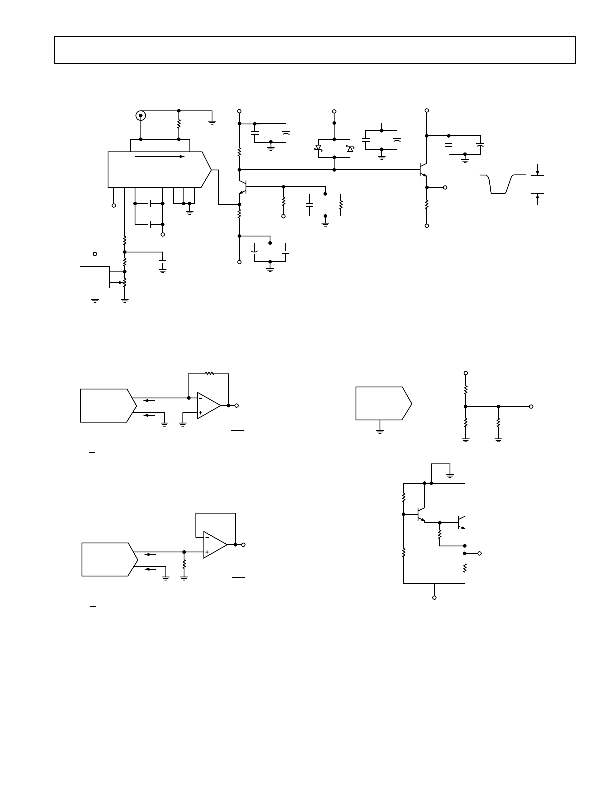
Figure 14. Settling Time Measurement
51
V
2.5kV
2.5kV
10kV
1MV
1/4W, 5%
CARBON
2kV
4kV
1kV
499kV
1/4W, 5% CARBON
0.01mF
1mF
0.01mF
0.1mF10mF
4.7mF
0.01mF
1mF
0.01mF 4.7mF
0.1mF10mF
+15V
V
L
0.500V 60.001V
+15V
–15V
V
O
–15V
+15V
15 16 18
3
17 1 2
5
14
4
2
6
5
4
REF-01
–15V
–15V
175mV
2N918
2N918
LOW-TO-HIGH SETTLING V
L
= 16.500V 60.001V
HIGH-TO-LOW SETTLING V
L
= 0.500V 60.001V
1/2 LSB SETTLING = 7.8mV
NOTES:
1. CASE OF 2N918s MUST BE GROUNDED.
2. RESISTORS ARE 1/4W MF, 1% UNLESS OTHERWISE SPECIFIED.
3. USE FET PROBE (7A11 SCOPE PLUGIN).
D.U.T.
IN5711
DAC10
R
L
I
4
O
DAC10
FOR COMPLEMENTARY OUTPUT (OPERATION AS A NEGATIVE
LOGIC DAC), CONNECT INVERTING INPUT OF OP AMP TO
IO (PIN 2); CONNECT IO (PIN 4) TO GROUND.
I
O
2
E
OOP01
0 TO +IFR 3 R
1023
I
=
3 2 3 I
FR
1024
L
REF
V
TH
DAC10
TTL
= +1.4V
V
LC
1
ECL
+15V
9.1kV
6.2kV 0.1mF
= VLC +1.4V
V
TH
+15V CMOS
= +7.6V
V
TH
Figure 15. Positive Low Impedance Output Operation
13kV
2N3904
"A"
E
I
4
O
DAC10
FOR COMPLEMENTARY OUTPUT (OPERATION AS A NEGATIVE
LOGIC DAC), CONNECT NOINVERTING INPUT OF OP AMP TO
PIN 2); CONNECT IO (PIN 4) TO GROUND.
I
O
Figure 16. Negative Low Impedance Output Operation Figure 17. Interfacing with Various Logic Families
REV. D
I
O
2
OP15
R
0 TO –IFR 3 R
L
I
FR
O
1023
=
3 2 3 I
1024
L
REF
–7–
39kV
–5.2V
3kV
2N3904
TO PIN 1
6.2kV
V
LC
V
LC
Page 8
DAC10
APPLICATIONS
+V
REF
OPTIONAL RESISTOR
R
REF
R
IN
0V
TYPICAL VALUES:
R
= 1kV
IN
+VIN = 2V
R
EQ
1
1
1
+
=
+
R
R
P
IN
REQ = 800V
R
P
1
R
REF
FOR OFFSET INPUTS
16
DAC10
17
NO CAP
R
L
4
R
L
2
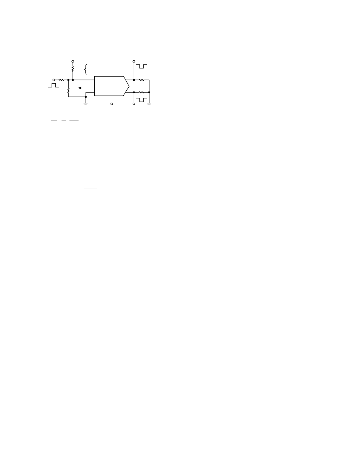
Figure 18. Pulsed Reference Operation
Reference Amplifier Setup
The DAC10 is a multiplying D/A converter in which the output
current is the product of a digital number and the input reference current. The reference current may be fixed or may vary
from nearly zero to 2 mA. The full-scale output current is a
linear function of the reference current and is given by:
1023
I
where I
=
FR
equals current flowing into Pin 16.
REF
1024
×2 × I
REF
In positive reference applications, an external positive reference
voltage forces current through R16 into the V
(+) terminal
REF
(Pin 16) of the reference amplifier. Alternatively, a negative
reference may be applied to V
(–) at Pin 17; reference current
REF
flows from ground through R16 into V(+) as in the positive
reference case. This negative reference connection has the advantage of a very high impedance presented at Pin 17. R17
(nominally equal to R16) is used to cancel bias current errors;
R17 may be eliminated with only a minor increase in error.
Bipolar references may be accommodated by offsetting V
REF
or
Pin 17. The negative common-mode range of the reference
amplifier is given by: V
– = V– plus (I
CM
× 2 kΩ) plus 2 V.
REF
The positive common-mode range is V+ less 1.8 V.
When a dc reference is used, a reference bypass capacitor is
recommended. A 5 V TTL logic supply is not recommended as
a reference. If a regulated power supply is used as a reference,
R16 should be split into two resistors with the junction bypassed
to ground with a 0.1 µF capacitor.
For most applications, the tight relationship between I
I
will eliminate the need for trimming I
FS
. If required, full-
REF
REF
and
scale trimming may be accomplished by adjusting the value of
R16, or by using a potentiometer for R16. An improved method
of full-scale trimming that eliminates potentiometer TC effect is
shown in the Recommended Full-Scale Adjustment circuit.
The reference amplifier must be compensated by using a capacitor from Pin 18 to V–. For fixed reference operation, a 0.01 µF
capacitor is recommended. For variable reference applications,
see section entitled Reference Amplifier Compensation for Multiplying Applications.
Multiplying Operation
The DAC10 provides excellent multiplying performance with an
extremely linear relationship between I
and I
FS
over a range
REF
of 4 mA to 4 µA. Monotonic operation is maintained over a
typical range of I
from 100 µA to 2 mA.
REF
Reference Amplifier Compensation for Multiplying Applications
AC reference applications will require the reference amplifier to
be compensated using a capacitor from Pin 18 to V–. The value
of this capacitor depends on the impedance presented to Pin 16
for R16 values of 1.0 kΩ, 2.5 kΩ and 5.0 kΩ, minimum values
of C
are 15 pF, 37 pF and 75 pF. Larger values of R16 require
C
proportionately increased values of C
for proper phase margin.
C
For fastest response to a pulse, low values of R16 enabling small
C
values should be used. If Pin 16 is driven by a high imped-
C
ance such as a transistor current source, none of the above values will suffice and the amplifier must be heavily compensated,
which will decrease overall bandwidth and slew rate. For R16 =
1kΩ and C
enabling a transition from I
= 15 pF, the reference amplifier slews at 4 mA/µs
C
= 0 to I
REF
= 2 mA in 500 ns.
REF
Operation with pulse inputs to the reference amplifier may be
accommodated by an alternate compensation scheme. This
technique provides lowest full-scale transition times. An internal
clamp allows quick recovery of the reference amplifier from a
cutoff (I
= 0) condition. Full-scale transition (0 mA to 2 mA)
REF
occurs in 120 ns when the equivalent impedance at Pin 16 is
200 Ω and C
µs, which is relatively independent of R
= 0. This yields a reference slew rate of 16 mA/
C
and VIN values.
IN
LOGIC INPUTS
The DAC10 design incorporates a unique logic input circuit
that enables direct interface to all popular logic families and
provides maximum noise immunity. This feature is made possible by the large input swing capability, 2 µA logic input current
and completely adjustable logic threshold voltage. For V– = –15 V,
the logic inputs may swing between –5 and +18 V. This enables
direct interface with +15 V CMOS logic, even when the DAC10
is powered from a +5 V supply. Minimum input logic swing and
minimum logic threshold voltage are given by: V– plus (l
REF
×
2kΩ) plus 3 V. The logic threshold may be adjusted over a wide
range by placing an appropriate voltage at the logic threshold
control Pin (Pin 1, V
relationship between V
with V
nominally 1.4 V above VLC. For TTL interface, simply
TH
ground Pin 1. When interfacing ECL, an I
). The appropriate graph shows the
LC
and VTH over the temperature range,
LC
= 1 mA is recom-
REF
mended. For interfacing other logic families, see Figure 17. For
general setup of the logic control circuit, it should be noted that
Pin 1 will sink 1.1 mA typical; external circuitry should be designed to accommodate this current.
Fastest settling times are obtained when Pin 1 sees a low impedance. If Pin 1 is connected to a 1 kΩ divider, for example, it
should be bypassed to ground by a 0.01 µF capacitor.
–8–
REV. D
Page 9

DAC10
ANALOG OUTPUT CURRENTS
Both true and complemented output sink currents are provided
where
I
O+IO
when a “1” is applied to each logic input. As the binary count
. Current appears at the “true” output
= I
FS
increases, the sink current at Pin 4 increases proportionally, in
the fashion of a “positive logic” D/A converter. When a “0” is
applied to any input bit, that current is turned off at Pin 4 and
turned on at Pin 2. A decreasing logic count increases
a negative or inverted logic D/A converter. Both outputs may be
I
O
as in
used simultaneously. If one of the outputs is not required, it
must still be connected to ground or to a point capable of sourcing I
. DO NOT LEAVE AN UNUSED OUTPUT PIN OPEN.
FS
Both outputs have an extremely wide voltage compliance enabling fast direct current-to-voltage conversion through a resistor tied to ground or other voltage source. Positive compliance
is 36 V above V– and is independent of the positive supply.
Negative compliance is +10 V above V–.
The dual outputs enable double the usual peak-to-peak load
swing when driving loads in quasi-differential fashion. This
feature is especially useful in cable driving, CRT deflection and
in other balanced applications such as driving center-tapped
coils and transformers.
POWER SUPPLIES
The DAC10 operates over a wide range of power supply voltages from a total supply of 9 V to 36 V. When operating with V–
supplies of –10 V or less, I
≤ 1 mA is recommended. Low
REF
reference current operation decreases power consumption and
increases negative compliance, reference amplifier negative
common-mode range, negative logic input range and negative
logic threshold range; consult the various figures for guidance.
For example, operation at –9 V with I
= 2 mA is not recom-
REF
mended because negative output compliance would be reduced
to near zero. Operation from lower supplies is possible, however
at least 8 V total must be applied to ensure turn-on of the internal bias network.
Symmetrical supplies are not required, as the DAC10 is quite
insensitive to variations in supply voltage. Battery operation is
feasible as no ground connection is required; however, an artificial ground may be used to ensure that logic swings, etc., remain
within acceptable limits.
TEMPERATURE PERFORMANCE
The nonlinearity and monotonicity specifications of the DAC10
are guaranteed to apply over the entire rated operating temperature range. Full-scale output current drift is tight, typically
+10 ppm/°C, with zero-scale output current and drift essentially
negligible compared to 1/2 LSB.
The temperature coefficient of the reference resistor, R14,
should match and track that of the output resistor for minimum
overall full-scale drift. Settling times of the DAC10 decrease
approximately 10% at –55°C; an increase of about 15% is typical at +125°C.
SETTLING TIME
The DAC10 is capable of extremely fast settling times; typically
85 ns at I
= 2 mA. Judicious circuit design and careful board
REF
layout must be employed to obtain full performance potential
during testing and application. The logic switch design enables
propagation delays of only 35 ns for each of the 10 bits. Settling
time to within 1/2 LSB of the LSB is therefore 35 ns, with each
progressively larger bit taking successively longer. The MSB
settles in 85 ns, thus determining the overall settling time of
130 ns. Settling to 8-bit accuracy requires about 60 ns to 78 ns.
The output capacitance of the DAC10, including the package, is
approximately 18 pF; therefore, the output RC time constant
dominates settling time if R
> 500 Ω.
L
Settling time and propagation delay are relatively insensitive to
logic input amplitude and rise and fall times, due to the high
gain of the logic switches. Settling time also remains essentially
constant for I
for lower I
values down to 1 mA, with gradual increases
REF
values. The principal advantage of higher I
REF
REF
values lies in the ability to attain a given output level with lower
load resistors, thus reducing the output RC time constant.
Measurement of settling time requires the ability to accurately
resolve ±2 µA; therefore, a 4 kΩ load is needed to provide ad-
equate drive for most oscilloscopes. The settling time fixture of
schematic titled “Settling Time Measurement” uses a cascode
design to permit driving a 4 kΩ load with less than 5 pF of para-
sitic capacitance at the measurement node. At I
values of less
REF
than 1 mA, excessive RC damping of the output is difficult to
prevent while maintaining adequate sensitivity. However, the
major carry from 0111111111 to 1000000000 provides an accurate indicator of settling time. This code change does not require the normal 6.2 time constants to settle to within ± 0.2% of
the final value, and thus settling times may be observed at lower
values of I
REF
.
DAC10 switching transients or “glitches” are very low and may
be further reduced by small capacitive loads at the output with a
minor sacrifice in settling time.
Fastest operation can be obtained by using short leads, minimizing output capacitance and load resistor values, and by adequate
bypassing at the supply, reference and V
terminals. Supplies
LC
do not require large electrolytic bypass capacitors as the supply
current drain is independent of input logic states; 0.1 µF capaci-
tors at the supply pins provide full transient protection.
REV. D
–9–
Page 10
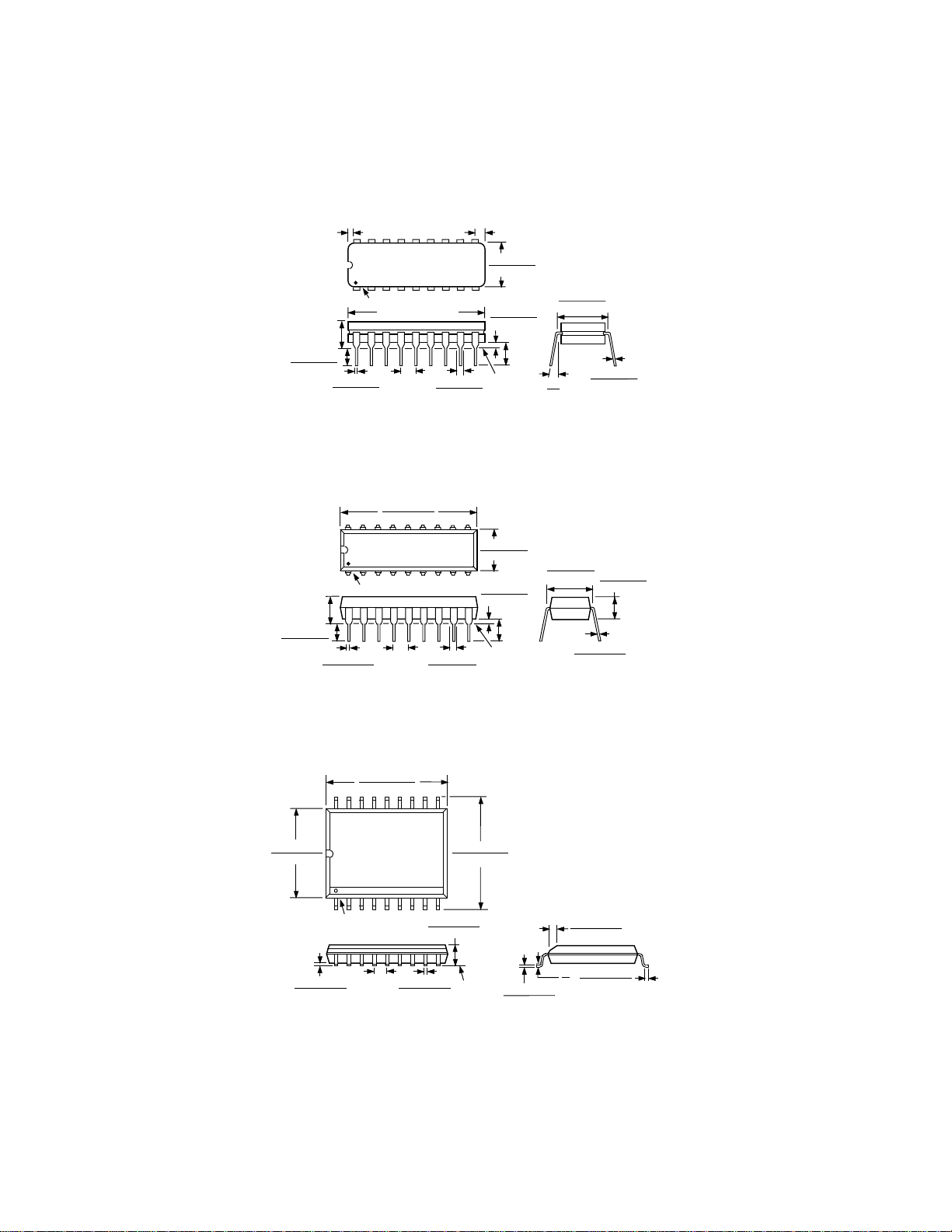
DAC10
OUTLINE DIMENSIONS
Dimensions shown in inches and (mm).
18-Lead Cerdip
(Q-18)
0.200 (5.08)
0.200 (5.08)
0.125 (3.18)
0.210
(5.33)
MAX
0.160 (4.06)
0.115 (2.93)
0.005 (0.13) MIN
18
1
PIN 1
MAX
0.023 (0.58)
0.014 (0.36)
0.960 (24.38) MAX
0.100
(2.54)
BSC
0.098 (2.49) MAX
10
9
0.070 (1.78)
0.030 (0.76)
0.310 (7.87)
0.220 (5.59)
0.060 (1.52)
0.015 (0.38)
SEATING
PLANE
18-Lead Plastic DIP
(N-18)
0.925 (23.49)
0.845 (21.47)
18
19
PIN 1
0.022 (0.558)
0.014 (0.356)
0.100
(2.54)
BSC
10
0.070 (1.77)
0.045 (1.15)
0.280 (7.11)
0.240 (6.10)
0.060 (1.52)
0.015 (0.38)
SEATING
PLANE
0.150
(3.81)
MIN
0.130
(3.30)
MIN
0.320 (8.13)
0.290 (7.37)
15°
0°
0.325 (8.25)
0.300 (7.62)
0.015 (0.381)
0.008 (0.204)
C3134–0–5/98
0.015 (0.38)
0.008 (0.20)
0.195 (4.95)
0.115 (2.93)
0.2992 (7.60)
0.2914 (7.40)
0.0118 (0.30)
0.0040 (0.10)
18-Lead Wide Body SOL
0.4625 (11.75)
0.4469 (11.35)
18 10
PIN 1
0.0500
(1.27)
BSC
0.1043 (2.65)
0.0926 (2.35)
0.0192 (0.49)
0.0138 (0.35)
(R-18)
0.4193 (10.65)
0.3937 (10.00)
91
SEATING
PLANE
0.0125 (0.32)
0.0091 (0.23)
0.0291 (0.74)
0.0098 (0.25)
0.0500 (1.27)
8°
0°
0.0157 (0.40)
x 45°
PRINTED IN U.S.A.
–10–
REV. D
 Loading...