

Page 1
March 2002
DAC0830/DAC0832
8-Bit µP Compatible, Double-Buffered D to A Converters
DAC0830/DAC0832 8-Bit µP Compatible, Double-Buffered D to A Converters
General Description
The DAC0830 is an advanced CMOS/Si-Cr 8-bit multiplying
DAC designed to interface directly with the 8080, 8048,
8085, Z80
silicon-chromium R-2R resistor ladder network divides the
reference current and provides the circuit with excellent
temperature tracking characteristics (0.05% of Full Scale
Range maximum linearity error over temperature). The circuit uses CMOS current switches and control logic to
achieve low power consumption and low output leakage
current errors. Special circuitry provides TTL logic input voltage level compatibility.
Double buffering allows these DACs to output a voltage
corresponding to one digital word while holding the next
digital word. This permits the simultaneous updating of any
number of DACs.
The DAC0830 series are the 8-bit members of a family of
microprocessor-compatible DACs (MICRO-DAC
®
, andother popular microprocessors.Adeposited
™
).
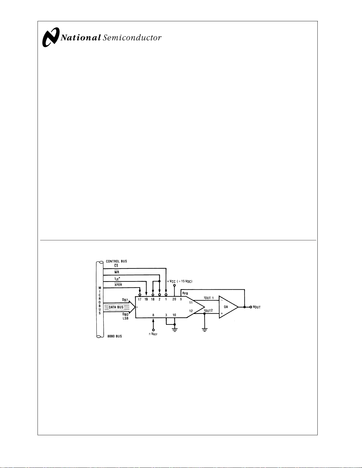
Typical Application
Features
n Double-buffered, single-buffered or flow-through digital
data inputs
n Easy interchange and pin-compatible with 12-bit
DAC1230 series
n Direct interface to all popular microprocessors
n Linearity specified with zero and full scale adjust
only—NOT BEST STRAIGHT LINE FIT.
n Works with
n Can be used in the voltage switching mode
n Logic inputs which meet TTL voltage level specs (1.4V
logic threshold)
n Operates “STAND ALONE” (without µP) if desired
n Available in 20-pin small-outline or molded chip carrier
package
±
10V reference-full 4-quadrant multiplication
Key Specifications
n Current settling time: 1 µs
n Resolution: 8 bits
n Linearity: 8, 9, or 10 bits (guaranteed over temp.)
n Gain Tempco: 0.0002% FS/˚C
n Low power dissipation: 20 mW
n Single power supply: 5 to 15 V
DC
00560801
BI-FET™and MICRO-DAC™are trademarks of National Semiconductor Corporation.
®
Z80
is a registered trademark of Zilog Corporation.
© 2002 National Semiconductor Corporation DS005608 www.national.com
Page 2
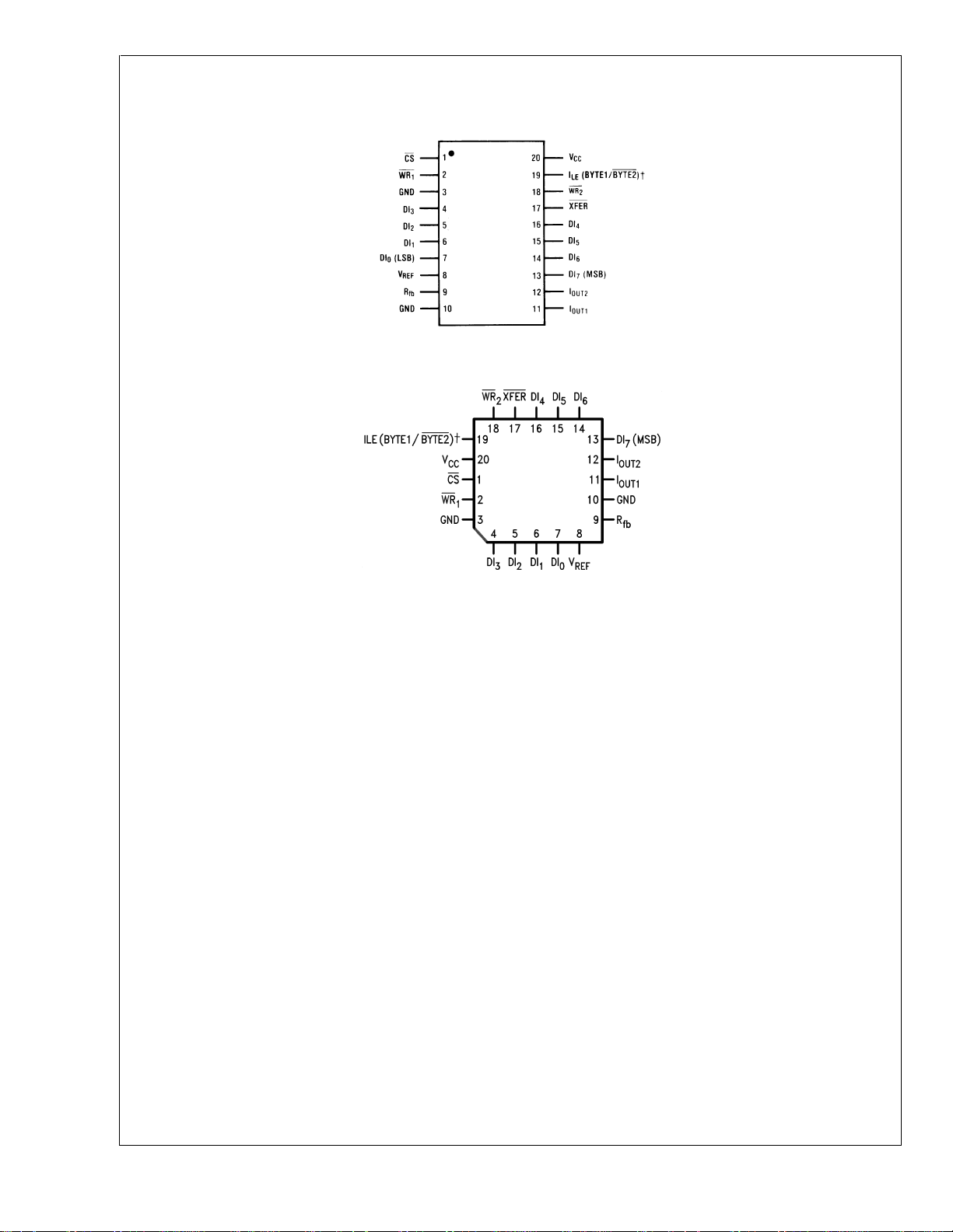
Connection Diagrams (Top Views)
DAC0830/DAC0832
Dual-In-Line and
Small-Outline Packages
00560821
Molded Chip Carrier Package
00560822
www.national.com 2
Page 3
DAC0830/DAC0832
Absolute Maximum Ratings (Notes 1,
2)
If Military/Aerospace specified devices are required,
please contact the National Semiconductor Sales Office/
Distributors for availability and specifications.
Supply Voltage (V
Voltage at Any Digital Input VCCto GND
Voltage at V
REF
Storage Temperature Range −65˚C to +150˚C
Package Dissipation
at T
=25˚C (Note 3) 500 mW
A
DC Voltage Applied to
I
or I
OUT1
OUT2
ESD Susceptability (Note 4) 800V
Lead Temperature (Soldering, 10 sec.)
)17V
CC
Input
(Note 4) −100 mV to V
±
DC
25V
CC
Dual-In-Line Package (plastic) 260˚C
Dual-In-Line Package (ceramic) 300˚C
Surface Mount Package
Vapor Phase (60 sec.) 215˚C
Infrared (15 sec.) 220˚C
Operating Conditions
Temperature Range T
Part numbers with “LCN” suffix 0˚C to +70˚C
Part numbers with “LCWM” suffix 0˚C to +70˚C
Part numbers with “LCV” suffix 0˚C to +70˚C
Part numbers with “LCJ” suffix −40˚C to +85˚C
Part numbers with “LJ” suffix −55˚C to +125˚C
Voltage at Any Digital Input V
MIN≤TA≤TMAX
CC
to GND
Electrical Characteristics
V
=10.000 VDCunless otherwise noted. Boldface limits apply over temperature, T
REF
T
=25˚C.
A
Parameter Conditions
See
Note
V
= 4.75 V
CC
VCC= 15.75 V
Typ
(Note 12)
MIN≤TA≤TMAX
DC
DC
Tested
Limit
(Note 5)
CONVERTER CHARACTERISTICS
Resolution 8 8 8 bits
Linearity Error Max Zero and full scale adjusted 4, 8
REF
≤+10V
−10V≤V
DAC0830LJ & LCJ 0.05 0.05 % FSR
DAC0832LJ & LCJ 0.2 0.2 % FSR
DAC0830LCN, LCWM &
0.05 0.05 % FSR
LCV
DAC0831LCN 0.1 0.1 % FSR
DAC0832LCN, LCWM &
0.2 0.2 % FSR
LCV
Differential Nonlinearity Zero and full scale adjusted 4, 8
Max −10V≤V
REF
≤+10V
DAC0830LJ & LCJ 0.1 0.1 % FSR
DAC0832LJ & LCJ 0.4 0.4 % FSR
DAC0830LCN, LCWM &
0.1 0.1 % FSR
LCV
DAC0831LCN 0.2 0.2 % FSR
DAC0832LCN, LCWM &
0.4 0.4 % FSR
LCV
Monotonicity −10V≤V
≤+10V LCN, LCWM &
LJ & LCJ 4 88bits
REF
8 8 bits
LCV
Gain Error Max Using Internal R
−10V≤V
REF
≤+10V
Gain Error Tempco Max Using internal R
fb
fb
7
±
0.2
0.0002 0.0006 %
±
1
. For all other limits
VCC=5V
V
to 15 V
CC
DC
=12V
±
5%
±
DC
Design
Limit
(Note 6)
±
1 %FS
±
DC
5%
5%
Limit
Units
www.national.com3
Page 4
Electrical Characteristics (Continued)
V
=10.000 VDCunless otherwise noted. Boldface limits apply over temperature, T
REF
T
=25˚C.
A
DAC0830/DAC0832
Parameter Conditions
See
Note
V
= 4.75 V
CC
VCC= 15.75 V
Typ
(Note 12)
MIN≤TA≤TMAX
DC
DC
Tested
Limit
(Note 5)
CONVERTER CHARACTERISTICS
Power Supply Rejection All digital inputs latched high
=14.5V to 15.5V 0.0002 0.0025 %
V
CC
11.5V to 12.5V 0.0006 FSR/V
4.5V to 5.5V 0.013 0.015
Reference Max 15 20 20 kΩ
Input Min 15 10 10 kΩ
Output Feedthrough
Error
Output
I
Leakage
Current Max
I
OUT1
OUT2
V
=20 Vp-p, f=100 kHz
REF
All data inputs latched low
3 mVp-p
All data inputs LJ & LCJ 10 100 100 nA
latched low LCN, LCWM &
50 100
LCV
All data inputs LJ & LCJ 100 100 nA
latched high LCN, LCWM &
50 100
LCV
Output I
Capacitance I
OUT1
OUT2
I
OUT1
I
OUT2
All data inputs 45 pF
latched low 115
All data inputs 130 pF
latched
30
high
DIGITAL AND DC CHARACTERISTICS
Digital Input Max Logic Low LJ: 4.75V 0.6
Voltages LJ: 15.75V 0.8
LCJ: 4.75V 0.7 V
LCJ: 15.75V 0.8
LCN, LCWM, LCV 0.95 0.8
Min Logic High LJ & LCJ 2.0 2.0 V
LCN, LCWM, LCV 1.9 2.0
Digital Input Max Digital inputs
<
0.8V
Currents LJ & LCJ −50 −200 −200 µA
LCN, LCWM, LCV −160 −200 µA
Digital inputs
>
2.0V
LJ & LCJ 0.1 +10 +10 µA
LCN, LCWM, LCV +8 +10
Supply Current Max LJ & LCJ 1.2 3.5 3.5 mA
Drain LCN, LCWM, LCV 1.7 2.0
. For all other limits
VCC=5V
V
to 15 V
CC
DC
=12V
±
5%
±
DC
Design
Limit
(Note 6)
±
DC
5%
5%
Limit
Units
FS/˚C
DC
DC
www.national.com 4
Page 5

Electrical Characteristics
V
=10.000 VDCunless otherwise noted. Boldface limits apply over temperature, T
REF
T
A
=25˚C.
MIN≤TA≤TMAX
VCC=12
Symbol Parameter Conditions
See
Note
=15.75 V
V
CC
Typ
(Note 12)
DC
Tested
Limit
(Note 5)
±
5% to 15
V
DC
±
5%
V
DC
Design Limit
(Note 6)
V
Typ
(Note 12)
AC CHARACTERISTICS
t
s
Current Setting VIL=0V,
=5V
V
IH
1.0 1.0 µs
Time
t
W
Write and XFER VIL=0V,
=5V
V
IH
11 100 250 375 600
Pulse Width Min 9 320 320 900 900
t
DS
Data Setup Time VIL=0V,
=5V
V
IH
100 250 375 600
9
Min 320 320 900 900
t
DH
Data Hold Time VIL=0V,
=5V
V
IH
9
30 50
Min 30 50
t
CS
Control Setup
Time
VIL=0V,
=5V
V
IH
110 250 600 900
9
Min 320 320 1100 1100
t
CH
Control Hold Time VIL=0V,
=5V
V
IH
90
0
10 0
Min 00
Note 1: Absolute Maximum Ratings indicate limits beyond which damage to the device may occur.DC and AC electrical specifications do not apply when operating
the device beyond its specified operating conditions.
Note 2: All voltages are measured with respect to GND, unless otherwise specified.
Note 3: The maximum power dissipation must be derated at elevated temperatures and is dictated by T
allowable power dissipation at any temperature is P
= 125˚C (plastic) or 150˚C (ceramic), and the typical junction-to-ambient thermal resistance of the J package when board mounted is 80˚C/W. For the N
T
JMAX
package, this number increases to 100˚C/W and for the V package this number is 120˚C/W.
Note 4: For current switching applications, both I
by approximately V
Note 5: Tested limits are guaranteed to National’s AOQL (Average Outgoing Quality Level).
Note 6: Guaranteed, but not 100% production tested. These limits are not used to calculate outgoing quality levels.
Note 7: Guaranteed at V
Note 8: The unit “FSR” stands for “Full Scale Range.” “Linearity Error” and “Power Supply Rejection” specs are based on this unit to eliminate dependence on a
particular V
that after performing a zero and full scale adjustment (see Sections 2.5 and 2.6), the plot of the 256 analog voltage outputs will each be within 0.05%xV
straight line which passes through zero and full scale.
Note 9: Boldface tested limits apply to the LJ and LCJ suffix parts only.
Note 10: A 100nA leakage current with R
Note 11: The entire write pulse must occur within the valid data interval for the specified t
Note 12: Typicals are at 25˚C and represent most likely parametric norm.
Note 13: Human body model, 100 pF discharged through a 1.5 kΩ resistor.
OS÷VREF
value and to indicate the true performance of the part. The “Linearity Error” specification of the DAC0830 is “0.05% of FSR (MAX)”. This guarantees
REF
. For example, if V
=±10 VDCand V
REF
fb
=(T
D
and I
OUT1
=10Vthena1mVoffset, VOS,onI
REF
=±1VDC.
REF
=20k and V
REF
)/θJAor the number given in theAbsolute Maximum Ratings, whichever is lower. For this device,
JMAX−TA
must go to ground or the “Virtual Ground” of an operational amplifier.The linearity error is degraded
OUT2
=10V corresponds to a zero error of (100x10−9x20x103)x100/10 which is 0.02% of FS.
or I
OUT1
W,tDS,tDH
, θJA, and the ambient temperature, TA. The maximum
JMAX
will introduce an additional 0.01% linearity error.
OUT2
, and tSto apply.
. For all other limits
=4.75 V
CC
Tested
Limit
(Note 5)
DC
VCC=5
V
DC
±
5%
Design
Limit
(Note 6)
0
REF
DAC0830/DAC0832
Limit
Units
ns
of a
www.national.com5
Page 6
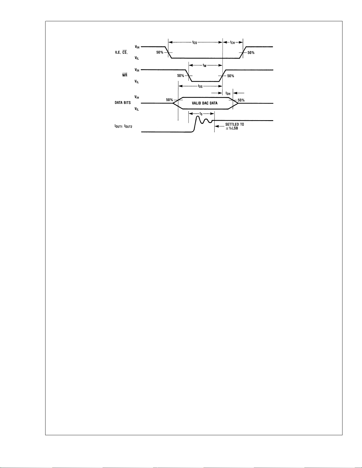
Switching Waveform
DAC0830/DAC0832
00560802
www.national.com 6
Page 7
Definition of Package Pinouts
Control Signals
(All control signals level actuated)
CS:
Chip Select (active low). The CS in combination
with ILE will enable WR1.
ILE: Input Latch Enable (active high). The ILE in com-
bination with CS enables WR
WR1: Write 1. The active low WR1is used to load the
digital input data bits (DI) into the input latch. The
data in the input latch is latched when WR
To update the input latch–CS and WR1must be low
while ILE is high.
WR
: Write 2 (active low). This signal, in combination with
2
XFER, causes the 8-bit data which is available in the
input latch to transfer to the DAC register.
XFER:
Transfer control signal (active low). The XFER will
enable WR2.
Other Pin Functions
DI
-DI7: Digital Inputs. DI0is the least significant bit (LSB)
0
and DI
I
: DAC Current Output 1. I
OUT1
is the most significant bit (MSB).
7
digital code of all 1’s in the DAC register, and is
zero for all 0’s in DAC register.
I
: DAC Current Output 2. I
OUT2
I
OUT1
,orI
OUT1+IOUT2
fixed reference voltage).
R
: Feedback Resistor. The feedback resistor is pro-
fb
vided on the IC chip for use as the shunt feedback
.
1
is high.
1
is a maximum for a
OUT1
is a constant minus
OUT2
= constant (I full scale for a
resistor for the external op amp which is used to
provide an output voltage for the DAC. This on-chip
resistor should always be used (not an external
resistor) since it matches the resistors which are
used in the on-chip R-2R ladder and tracks these
resistors over temperature.
: Reference Voltage Input. This input connects an
V
REF
external precision voltage source to the internal
R-2R ladder. V
can be selected over the range
REF
of +10 to −10V.This is also theanalog voltage input
for a 4-quadrant multiplying DAC application.
V
: Digital Supply Voltage. This is the power supply
CC
pin for the part. V
Operation is optimum for +15V
can be from +5 to +15VDC.
CC
DC
GND: The pin 10 voltage must be at the same ground
potential as I
applications. Any difference of potential (V
OUT1
and I
for current switching
OUT2
pin
OS
10) will result in a linearity change of
For example, if V
I
and I
OUT1
OUT2
Pin 3 can be offset
= 10V and pin 10 is 9mV offset from
REF
the linearity change will be 0.03%.
±
100mV with no linearity change, but the
logic input threshold will shift.
DAC0830/DAC0832
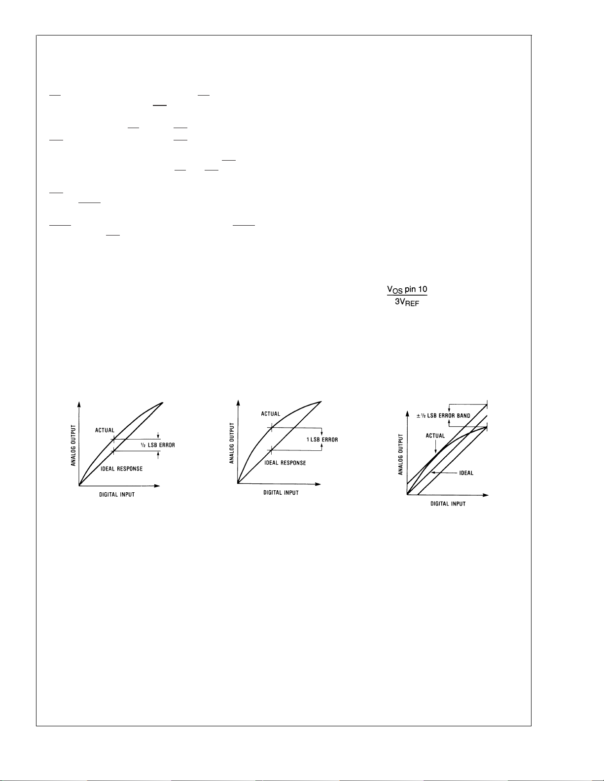
Linearity Error
a) End point test afterzero and fs
00560823
adj.
b) Best straight line
Definition of Terms
Resolution: Resolution is directly related to the number of
switches or bits within the DAC. For example, the DAC0830
8
has 2
or 256 steps and therefore has 8-bit resolution.
Linearity Error: Linearity Error is the maximum deviation
from a
straight line passing through the endpoints of the
DAC transfer characteristic
zero and full-scale. Linearity error is a parameter intrinsic to
the device and cannot be externally adjusted.
National’s linearity “end point test” (a) and the “best straight
line” test (b,c) used by other suppliers are illustrated above.
The “end point test’’ greatly simplifies the adjustment procedure by eliminating the need for multiple iterations of checking the linearity and then adjusting full scale until the linearity
is met. The “end point test’’ guarantees that linearity is met
. It is measured after adjusting for
00560824
00560825
c) Shifting fs adj. to pass
best straight line test
after a single full scale adjust. (One adjustment vs. multiple
iterations of the adjustment.) The “end point test’’ uses a
standard zero and F.S. adjustment procedure and is a much
more stringent test for DAC linearity.
Power Supply Sensitivity: Power supply sensitivity is a
measure of the effect of power supply changes on the DAC
full-scale output.
Settling Time: Settling time is the time required from a code
transition until the DAC output reaches within
1
±
⁄2LSB of the
final output value. Full-scale settling time requires a zero to
full-scale or full-scale to zero output change.
Full Scale Error: Full scale error is a measure of the output
error between an ideal DAC and the actual device output.
www.national.com7
Page 8
Definition of Terms (Continued)
Ideally, for the DAC0830 series, full scale is V
For V
10,0000V–39mV 9.961V. Full-scale error is adjustable to
zero.
Differential Nonlinearity: The difference between any two
consecutive codes in the transfer curve from the theoretical
DAC0830/DAC0832
1 LSB to differential nonlinearity.
= 10V and unipolar operation, V
REF
−1LSB.
REF
FULL-SCALE
Monotonic: If the output of a DAC increases for increasing
digital input code, then the DAC is monotonic. An 8-bit DAC
which is monotonic to 8 bits simply means that increasing
=
digital input codes will produce an increasing analog output.
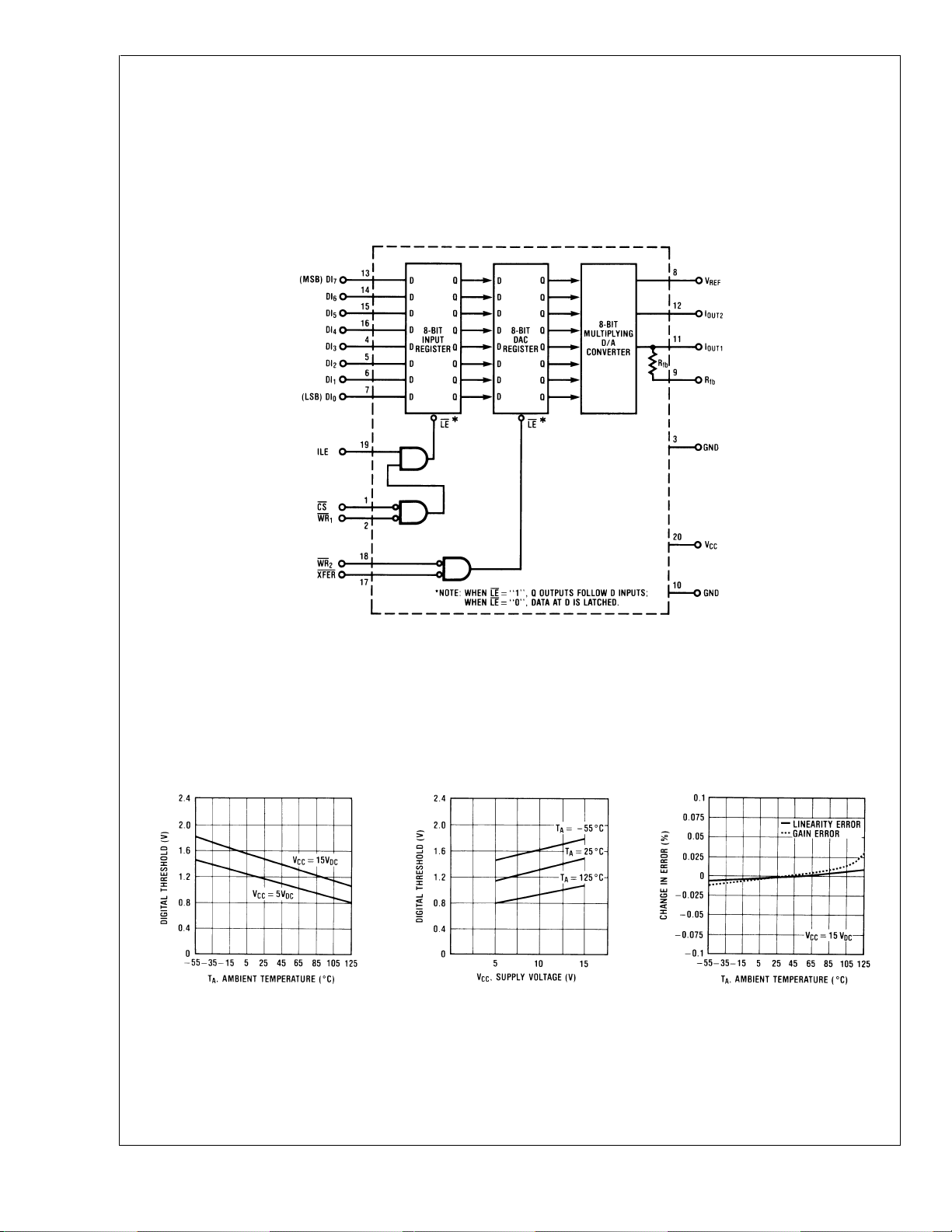
Typical Performance Characteristics
Digital Input Threshold
vs. Temperature
00560826
FIGURE 1. DAC0830 Functional Diagram
Digital Input Threshold
vs. V
CC
00560827
00560804
Gain and Linearity Error
Variation vs. Temperature
00560828
www.national.com 8
Page 9
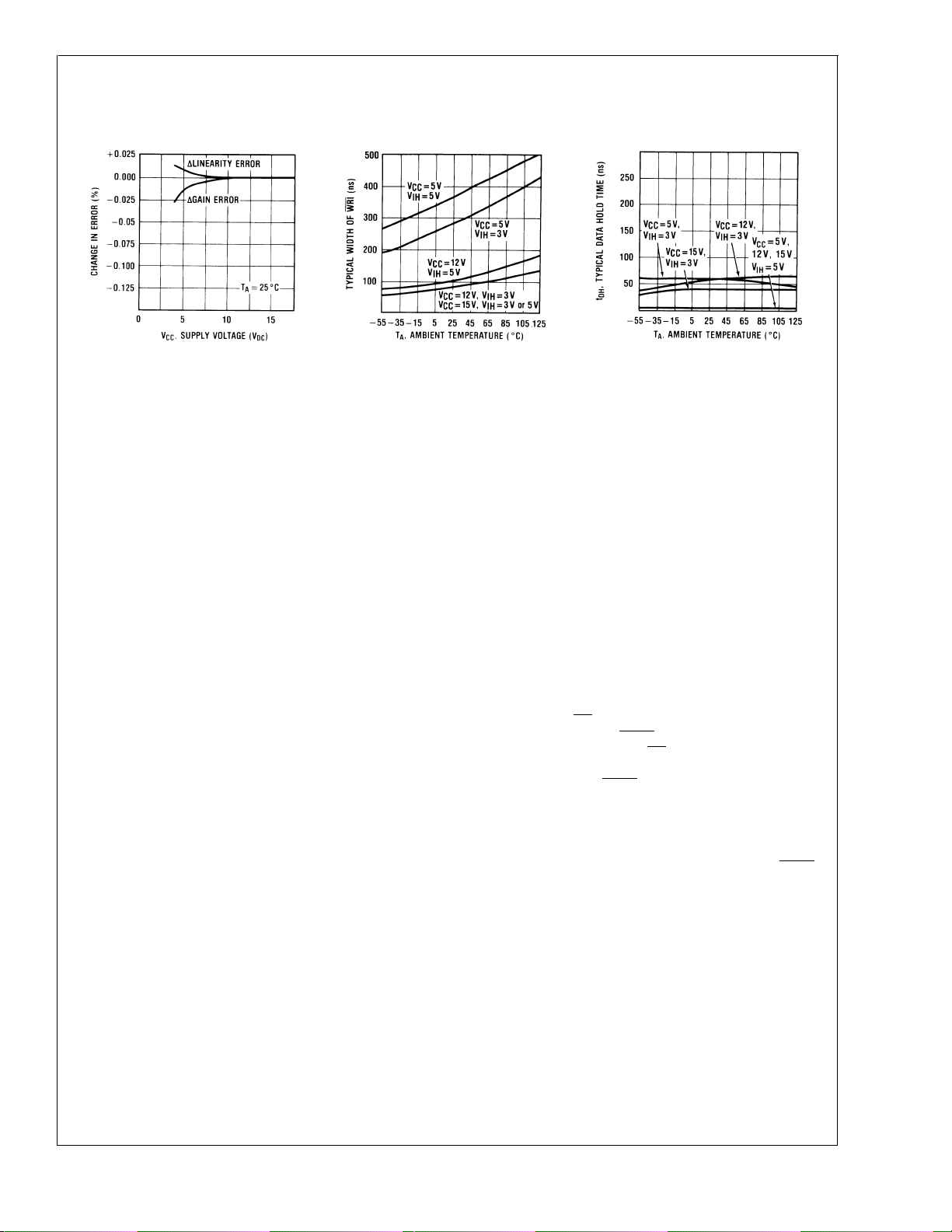
Typical Performance Characteristics (Continued)
DAC0830/DAC0832
Gain and Linearity Error
Write Pulse Width
Variation vs. Supply Voltage
00560829 00560830 00560831
DAC0830 Series Application Hints
These DAC’s are the industry’s first microprocessor compatible, double-buffered 8-bit multiplying D to A converters.
Double-buffering allows the utmost application flexibility from
a digital control point of view. This 20-pin device is also pin
for pin compatible (with one exception) with the DAC1230, a
12-bit MICRO-DAC. In the event that a system’s analog
output resolution and accuracy must be upgraded, substituting the DAC1230 can be easily accomplished. By tying
address bit A
(double precision) which automatically increments the address for the second byte write (starting with A
used. This allows either an 8-bit or the 12-bit part to be used
with no hardware or software changes. For the simplest 8-bit
application, this pin should be tied to V
uses in section 1.1).
Analog signal control versatility is provided by a precision
R-2R ladder network which allows full 4-quadrant multiplication of a wide range bipolar reference voltage by an applied
digital word.
1.0 DIGITAL CONSIDERATIONS
A most unique characteristic of these DAC’s is that the 8-bit
digital input byte is double-buffered. This means that the
data must transferthrough two independently controlled 8-bit
latching registers before being applied to the R-2R ladder
network to change the analog output. The addition of a
second register allows two useful control features. First, any
DAC in a system can simultaneously hold the current DAC
data in one register (DAC register) and the next data word in
the second register (input register) to allow fast updating of
the DAC output on demand. Second, and probably more
important, double-buffering allows any number of DAC’s in a
system to be updated to their new analog output levels
simultaneously via a common strobe signal.
to the ILE pin, a two-byte µP write instruction
0
=“1”) can be
0
(also see other
CC
Data Hold Time
The timing requirements and logic level convention of the
register control signals have been designed to minimize or
eliminate external interfacing logic when applied to most
popular microprocessors and development systems. It is
easy to think of these converters as 8-bit “write-only”
memory locations that provide an analog output quantity. All
inputs to these DAC’s meet TTL voltage level specs and can
also be driven directly with high voltage CMOS logic in
non-microprocessor based systems. To prevent damage to
the chip from static discharge, all unused digital inputs
should be tied to V
or ground. If any of the digital inputs
CC
are inadvertantly left floating, the DAC interprets the pin as a
logic “1”.
1.1 Double-Buffered Operation
Updating the analog output of these DAC’s in a
double-buffered manner is basically a two step or double
write operation. In a microprocessor system two unique
system addresses must be decoded, one for the input latch
controlled by the CS pin and a second for the DAC latch
which is controlled by the XFER line. If more than one DAC
is being driven,
Figure 2
, the CS line of each DAC would
typically be decoded individually, but all of the converters
could share a common XFER address to allow simultaneous
updating of any number of DAC’s. The timing for this operation is shown,
Figure 3
.
It is important to note that the analog outputs that will change
after a simultaneous transfer are those from the DAC’s
whose input register had been modified prior to the XFER
command.
www.national.com9
Page 10

DAC0830 Series Application Hints (Continued)
DAC0830/DAC0832
*
TIE TO LOGIC 1 IF NOT NEEDED (SEE SEC. 1.1).
FIGURE 2. Controlling Mutiple DACs
The ILE pin is an active high chip select which can be
decoded from the address bus as a qualifier for the normal
CS signal generated during a write operation. This can be
used to provide a higher degree of decoding unique control
signals for a particular DAC, and thereby create a more
efficient addressing scheme.
Another useful application of the ILE pin of each DAC in a
multiple DAC system is to tie these inputs together and use
this as a control line that can effectively “freeze” the outputs
of all the DAC’s at their present value. Pulling this line low
latches the input register and prevents new data from being
00560835
00560836
FIGURE 3.
written to the DAC. This can be particularly useful in multiprocessing systems to allow a processor other than the one
controlling the DAC’s to take over control of the data busand
control lines. If this second system were to use the same
addresses as those decoded for DAC control (but for a
different purpose) the ILE function would prevent the DAC’s
from being erroneously altered.
In a “Stand-Alone” system the control signals are generated
by discrete logic. In this case double-buffering can be controlled by simply taking CS and XFER to a logic “0”, ILE to a
logic “1” and pulling WR1low to load data to the input latch.
www.national.com 10
Page 11

DAC0830 Series Application Hints
(Continued)
DAC0830/DAC0832
Pulling WR
low will then update the analog output. A logic
2
“1” on either of these lines will prevent the changing of the
analog output.
ILE=LOGIC “1”; WR2 and XFER GROUNDED
1.2 Single-Buffered Operation
In a microprocessor controlled system where maximum data
throughput to the DAC is of primary concern, or when only
one DAC of several needs to be updated at a time, a
single-buffered configuration can be used. One of the two
internal registers allows the data to flow through and the
other register will serve as the data latch.
Digital signal feedthrough (see Section 1.5) is minimized if
the input register is used as the data latch. Timing for this
mode is shown in
Figure 4
.
Single-buffering in a “stand-alone” system is achieved by
strobing WR
low to update the DAC with CS, WR2and
1
XFER grounded and ILE tied high.
1.3 Flow-Through Operation
Though primarily designed to provide microprocessor interface compatibility, the MICRO-DAC’s can easily be configured to allow the analog output to continuously reflect the
state of an applied digital input. This is most useful in applications where the DAC is used in a continuous feedback
control loop and is driven by a binary up-down counter, or in
function generation circuits where a ROM is continuously
providing DAC data.
Simply grounding CS, WR
,WR2, and XFER and tying ILE
1
high allows both internal registers to follow the applied digital
inputs (flow-through) and directly affect the DAC analog
output.
1.4 Control Signal Timing
When interfacing these MICRO-DAC to any microprocessor,
there are two important time relationships that must be considered to insure proper operation. The first is the minimum
WR strobe pulse width which is specified as 900 ns for all
valid operating conditions of supply voltage and ambient
temperature, but typically a pulse width of only 180ns is
adequate if V
=15VDC. A second consideration is that the
CC
guaranteed minimum data hold time of 50ns should be met
FIGURE 4.
00560807
or erroneous data can be latched. This hold time is defined
as the length of time data must be held valid on the digital
after
inputs
a qualified (via CS) WR strobe makes a low to
high transition to latch the applied data.
If the controlling device or system does not inherently meet
these timing specs the DAC can be treated as a slow
memory or peripheral and utilize a technique to extend the
write strobe. A simple extension of the write time, by adding
a wait state, can simultaneously hold the write strobe active
and data valid on the bus to satisfy the minimum WR pulsewidth. If this does not provide a sufficient data hold time at
the end of the write cycle, a negative edge triggered
one-shot can be included between the system write strobe
and the WR pin of the DAC. This is illustrated in
Figure 5
for
an exemplary system which provides a 250ns WR strobe
time with a data hold time of less than 10ns.
The proper data set-up time prior to the latching edge (LO to
HI transition) of the WR strobe, is insured if the WR pulsewidth is within spec and the data is valid on the bus for the
duration of the DAC WR strobe.
1.5 Digital Signal Feedthrough
When data is latched in the internal registers, but the digital
inputs are changing state, a narrow spikeof current may flow
out of the current output terminals. This spike is caused by
the rapid switching of internal logic gates that areresponding
to the input changes.
There are several recommendations to minimize this effect.
When latching data in the DAC, always use the input register
as the latch. Second, reducing the V
supply for the DAC
CC
from +15V to +5V offers a factor of 5 improvement in the
magnitude of the feedthrough, but at the expense of internal
logic switching speed. Finally, increasing C
(
Figure 8
C
)toa
value consistent with the actual circuit bandwidth requirements can provide a substantial damping effect on any
output spikes.
www.national.com11
Page 12

DAC0830 Series Application Hints (Continued)
DAC0830/DAC0832
00560808
FIGURE 5. Accommodating a High Speed System
2.0 ANALOG CONSIDERATIONS
The fundamental purpose of any D to A converter is to
provide an accurate analog output quantity which is representative of the applied digital word. In the case of the
DAC0830, the output, I
, is a current directly proportional
OUT1
to the product of the applied reference voltage and the digital
input word. For application versatility, a second output,
I
, is provided as a current directly proportional to the
OUT2
complement of the digital input. Basically:
where the digital input is the decimal (base 10) equivalent of
the applied 8-bit binary word (0 to 255), V
is the voltage
REF
at pin 8 and 15 kΩ is the nominal value of the internal
resistance, R, of the R-2R ladder network (discussed in
Section 2.1).
Several factors external to the DAC itself must be considered to maintain analog accuracy and are covered in subsequent sections.
2.1 The Current Switching R-2R Ladder
The analog circuitry,
Figure 6
, consists of a silicon-chromium
(SiCr or Si-chrome) thin film R-2R ladder which is deposited
on the surface oxide of the monolithic chip. As a result, there
are no parasitic diode problems with the ladder (as there
may be with diffused resistors) so the reference voltage,
V
, can range −10V to +10V even if VCCfor the device is
REF
5V
.
DC
The digital input code to the DACsimply controls the position
of the SPDT current switches and steers the available ladder
current to either I
OUT1
or I
input level (“1” or “0”) respectively, as shown in
as determined by the logic
OUT2
Figure 6
. The
MOS switches operate in the current mode with a small
voltage drop across them and can therefore switch currents
of either polarity. This is the basis for the 4-quadrant multiplying feature of this DAC.
2.2 Basic Unipolar Output Voltage
To maintain linearity of output current with changes in the
applied digital code, it is important that the voltages at both
of the current output pins be as near ground potential (0V
as possible. With V
either I
OUT1
or I
=+10V every millivolt appearing at
REF
will cause a 0.01% linearity error. In
OUT2
DC
most applications this output current is converted to a voltage by using an op amp as shown in
Figure 7
.
The inverting inputof the op amp isa “virtual ground” created
by the feedback from its output through the internal 15 kΩ
resistor, R
. All of the output current (determined by the
fb
digital input and the reference voltage) will flow through R
to the output of the amplifier. Two-quadrant operation can be
obtained by reversing the polarity of V
thus causing I
REF
OUT1
to flow into the DAC and be sourced from the output of the
amplifier. The output voltage, in either case, is always equal
to I
OUT1xRfb
and is the opposite polarity of the reference
voltage.
The reference can be either a stable DC voltage source or
an AC signal anywhere in the range from −10V to +10V. The
DAC can be thought of as a digitally controlled attenuator:
the output voltage is always less than or equal to the applied
reference voltage. The V
terminal of the device presents
REF
a nominal impedance of 15 kΩ to ground to external circuitry.
)
fb
www.national.com 12
Page 13

DAC0830 Series Application Hints
(Continued)
DAC0830/DAC0832
Always use the internal R
resistor to create an output
fb
voltage since this resistor matches (and tracks with temperature) the value of the resistors used to generate the output
current (I
OUT1
).
00560837
FIGURE 6.
00560838
2.3 Op Amp Considerations
The op amp used in
Figure 7
should have offset voltage
nulling capability (See Section 2.5).
The selected op amp should have as low a value of input
bias current as possible. The product of the bias current
times the feedback resistance creates an output voltage
error which can be significant in low reference voltage applications. BI-FET
™
op amps are highly recommended for use
with these DACs because of their very low input current.
Transient response and settling time of the op amp are
important in fast data throughput applications. The largest
stability problem is the feedback pole created by the feedback resistance, R
, and the output capacitance of the DAC.
fb
This appears from the op amp output to the (−) input and
includes the stray capacitance at this node. Addition of a
lead capacitance, C
C
in
Figure 8
, greatly reduces overshoot
and ringing at the output for a step change in DAC output
current.
Finally, the output voltage swing of the amplifier must be
greater than V
to allow reaching the full scale output
REF
voltage. Depending on the loading on the output of the
amplifier and the available op amp supply voltages (only
±
12
volts in many development systems), a reference voltage
less than 10 volts may be necessary to obtain the full analog
output voltage range.
FIGURE 7.
2.4 Bipolar Output Voltage with a Fixed Reference
The addition of a secondop amp to the previous circuitry can
be used to generate a bipolar output voltage from a fixed
reference voltage. This, in effect, gives sign significance to
the MSB of the digital input word and allows two-quadrant
multiplication of the reference voltage. The polarity of the
reference can also be reversed to realize full 4-quadrant
multiplication:
shown in
±
Figure 9
V
x±Digital Code=±V
REF
.
. This circuit is
OUT
This configuration features several improvements over existing circuits for bipolar outputs with other multiplying DACs.
Only the offset voltage of amplifier 1 has to be nulled to
preserve linearity of the DAC. The offset voltage error of the
second op amp (although a constant output voltage error)
has no effect on linearity. It should be nulled only if absolute
output accuracy is required. Finally, the values of the resistors around the second amplifier do not have to match the
internal DAC resistors, they need only to match and temperature track each other. A thin film 4-resistor network
available from Beckman Instruments, Inc. (part no.
694-3-R10K-D) is ideally suited for this application. These
resistors are matched to 0.1% and exhibit only 5 ppm/˚C
resistance tracking temperature coefficient. Two of the four
available 10 kΩ resistors can be paralleled to form R in
Figure 9
and the other two can be used independently as the
resistances labeled 2R.
www.national.com13
Page 14

DAC0830 Series Application Hints
(Continued)
2.5 Zero Adjustment
For accurate conversions, the input offset voltage of the
output amplifier mustalways be nulled.Amplifier offset errors
create an overall degradation of DAC linearity.
DAC0830/DAC0832
The fundamental purpose of zeroing is to make the voltage
appearing at the DAC outputs as near 0V
DC
OP Amp C
LF356 22 pF 4 µs
LF351 22 pF 5 µs
LF357
*2.4 kΩ RESISTOR ADDED FROM−INPUT TO GROUND TO
INSURE STABILITY
as possible.
*
This is accomplished for the typical DAC — op amp connection (
resistor, and adjusting the V
op amp until the output reads zero volts. This is done, of
course, with an applied digital code of all zeros if I
driving the op amp (all one’s for I
is then removed and the converter is zero adjusted.
t
s
(O to Full Scale)
C
10 pF 2 µs
FIGURE 8.
Figure 7
) by shorting out Rfb, the amplifier feedback
nulling potentiometer of the
OS
OUT1
00560839
). The short around R
OUT2
is
fb
www.national.com 14
Page 15

DAC0830 Series Application Hints (Continued)
DAC0830/DAC0832
00560840
Input Code IDEAL V
MSB LSB +V
11111111
11000000
10000000
01111111
00111111
00000000
*THESE RESISTORS ARE AVAILABLE FROM BECKMAN INSTRUMENTS, INC. AS THEIR PART NO. 694-3-R10K-D
2.6 Full-Scale Adjustment
In the case where the matching of R
R-2R ladder (typically
±
0.2%) is insufficient for full-scale
accuracy in a particular application, the V
to the R value of the
fb
voltage can be
REF
adjusted or an external resistor and potentiometer can be
added as shown in
Figure 10
to provide a full-scale adjust-
ment.
The temperature coefficients of the resistors used for this
adjustment are of an important concern. To prevent degradation of the gain error temperature coefficient by the external resistors, their temperature coefficients ideally would
have to match that of the internal DAC resistors, which is a
highly impractical constraint. For the values shown in
10
, if the resistor and the potentiometer each had a tempera-
ture coefficient of
±
100 ppm/˚C maximum, the overall gain
Figure
REF
FIGURE 9.
OUT
−V
REF
error temperature coefficent would be degraded a maximum
of 0.0025%/˚C for an adjustment pot setting of less than 3%
.
of R
fb
2.7 Using the DAC0830 in a Voltage Switching Configuration
The R-2R ladder can also be operated as a voltage switching network. In this mode the ladder is used in an inverted
manner from the standard current switching configuration.
The reference voltage is connected to one of the current
output terminals (I
for true binary digital control, I
OUT1
OUT2
for complementary binary) and the output voltage is taken
from the normal V
voltage in the range from 0V to 255/256 V
of the applied digital code as shown in
pin. The converter output is now a
REF
as a function
REF
Figure 11
.
is
www.national.com15
Page 16

DAC0830 Series Application Hints (Continued)
DAC0830/DAC0832
FIGURE 10. Adding Full-Scale Adjustment
00560811
FIGURE 11. Voltage Mode Switching
This configuration offers several useful application advantages. Since the output is a voltage, an external op amp is
not necessarily required but the output impedance of the
DAC is fairly high (equal to the specified reference input
resistance of 10 kΩ to 20 kΩ) so an op amp may be used for
buffering purposes. Some of the advantages of this mode
are illustrated in
Figures 12, 13, 14, 15
.
There are two important things to keep in mind when using
this DAC in the voltage switching mode. The applied reference voltage must be positive since there are internal parasitic diodes from ground to the I
OUT1
and I
OUT2
terminals
which would turn on if the applied reference went negative.
There is also a dependence of conversion linearity and gain
error on the voltage difference between V
and the voltage
CC
applied to the normal current output terminals. This is a
result of the voltage drive requirements of the ladder
switches. Toensure that all 8 switches turn on sufficiently (so
as not to add significant resistance to any leg of the ladder
and thereby introduce additional linearity and gain errors) it
is recommended that the applied reference voltage be kept
less than +5V
V
. These restrictions ensure less than 0.1% linearity and
REF
gain error change.
fects of bringing V
and VCCbe at least 9V more positive than
DC
Figures 16, 17, 18
and VCCcloser together as well as
REF
characterize the ef-
typical temperature performance of this voltage switching
configuration.
00560812
Voltage switching mode eliminates output signal inver-
•
sion and therefore a need for a negative power supply.
Zero code output voltage is limited by the low level output
•
saturation voltage of the op amp. The 2 kΩ pull-down
resistor helps to reduce this voltage.
VOSof the op amp has no effect on DAC linearity.
•
00560841
www.national.com 16
FIGURE 12. Single Supply DAC
Page 17

DAC0830 Series Application Hints (Continued)
DAC0830/DAC0832
00560842
FIGURE 13. Obtaining a Bipolar Output from a Fixed Reference with a Single Op Amp
00560860
FIGURE 14. Bipolar Output with Increased Output Voltage Swing
www.national.com17
Page 18

DAC0830 Series Application Hints (Continued)
DAC0830/DAC0832
00560814
Gain and Linearity Error
Variation vs. Supply Voltage
Note: For these curves, V
pin 12 (I
OUT2
) grounded.
FIGURE 15. Single Supply DAC with Level Shift and Span- Adjustable Output
Gain and Linearity Error
Variation vs. Reference Voltage
is the voltage applied to pin 11 (I
REF
00560832
OUT1
) with
FIGURE 17.
FIGURE 16.
00560833
www.national.com 18
Page 19

DAC0830 Series Application Hints
(Continued)
Gain and Linearity Error
Variation vs. Temperature
00560834
FIGURE 18.
2.8 Miscellaneous Application Hints
These converters are CMOS products and reasonable care
should be exercised in handlingthem to prevent catastrophic
failures due to static discharge.
Conversion accuracy is only as good as the applied reference voltage so providing a stable source over time and
temperature changes is an important factor to consider.
A “good” ground is most desirable. A single point ground
distribution technique for analog signals and supply returns
keeps other devices in a system from affecting the output of
the DACs.
During power-up supply voltage sequencing, the −15V (or
−12V) supply of the op amp may appear first. This will cause
the output of the op amp to bias near the negative supply
potential. No harm is done to the DAC, however, as the
on-chip 15 kΩ feedback resistor sufficiently limits the current
flow from I
when this lead is internally clamped to one
OUT1
diode drop below ground.
Careful circuit construction with minimization of lead lengths
around the analog circuitry, is a primary concern. Good high
frequency supply decoupling will aid in preventing inadvertant noise from appearing on the analog output.
Overall noise reduction and reference stability is of particular
concern when using the higher accuracy versions, the
DAC0830 and DAC0831, or their advantages are wasted.
3.0 GENERAL APPLICATION IDEAS
The connections for the control pins of the digital input
registers are purposely omitted. Any of the control formats
discussed in Section 1 of the accompanying text will work
with any of the circuits shown.The method used depends on
the overall system provisions and requirements.
The digital input code is referred to as D and represents the
decimal equivalent value of the 8-bit binary input, for example:
Binary Input D
Pin 13 Pin 7 Decimal
MSB LSB Equivalent
11111111 255
10000000 128
00010000 16
00000010 2
00000000 0
DAC0830/DAC0832
www.national.com19
Page 20

Applications
DAC0830/DAC0832
DAC Controlled Amplifier (Volume Control)
00560843
www.national.com 20
Page 21

Applications (Continued)
DAC0830/DAC0832
Capacitance Multiplier
00560844
www.national.com21
Page 22

Applications (Continued)
DAC0830/DAC0832
Variable f
, Variable QO, Constant BW Bandpass Filter
O
00560817
www.national.com 22
Page 23

Applications (Continued)
DAC0830/DAC0832
DAC Controlled Function Generator
00560818
www.national.com23
Page 24

Applications (Continued)
DAC0830/DAC0832
Two Terminal Floating 4 to 20 mA Current Loop Controller
00560819
DAC0830 linearly controls the current flow from the input terminal to the output terminal to be 4 mA (for D=0) to 19.94 mA (for
•
D=255).
Circuit operates with a terminal voltage differential of 16V to 55V.
•
P2adjusts the magnitude of the output current and P1adjusts the zero to full scale range of output current.
•
Digital inputs can be supplied from a processor using opto isolators on each input or the DAC latches can flow-through
•
(connect control lines to pins 3 and 10 of the DAC) and the input data can be set by SPST toggle switches to ground (pins 3
and 10).
DAC Controlled Exponential Time Response
Output responds exponentially to input changes and automatically stops when V
•
www.national.com 24
00560820
OUT=VIN
Page 25

Applications (Continued)
Output time constant is directly proportional to the DAC input code and capacitor C
•
Input voltage must be positive (See section 2.7)
•
Ordering Information
Temperature Range 0˚C to +70˚ −40˚C to +85˚C −55˚C to +125˚C
Non
Linearity 0.1% FSR DAC0831LCN
Package Outline N20A—Molded
0.05%
FSR
0.2% FSR DAC0832LCN DAC0832LCWM DAC0832LCV DAC0832LCJ DAC0832LJ
DAC0830LCN DAC0830LCWM DAC0830LCV DAC0830LCJ DAC0830LJ
M20B Small Outline V20A Chip Carrier J20A—Ceramic DIP
DIP
DAC0830/DAC0832
www.national.com25
Page 26

Physical Dimensions inches (millimeters) unless otherwise noted
DAC0830/DAC0832
Ceramic Dual-In-Line Package (J)
Order Number DAC0830LCJ,
DAC0830LJ, DAC0832LJ or DAC0832LCJ
NS Package Number J20A
www.national.com 26
Page 27

Physical Dimensions inches (millimeters) unless otherwise noted (Continued)
DAC0830/DAC0832
Molded Small Outline Package (M)
Order Number DAC0830LCWM
or DAC0832LCWM
NS Package Number M20B
Molded Dual-In-Line Package (N)
Order Number DAC0830LCN,
or DAC0832LCN
NS Package Number N20A
www.national.com27
Page 28

Physical Dimensions inches (millimeters) unless otherwise noted (Continued)
Molded Chip Carrier (V)
Order Number DAC0830LCV
or DAC0832LCV
NS Package Number V20A
LIFE SUPPORT POLICY
NATIONAL’S PRODUCTS ARE NOT AUTHORIZED FOR USE AS CRITICAL COMPONENTS IN LIFE SUPPORT
DEVICES OR SYSTEMS WITHOUT THE EXPRESS WRITTEN APPROVAL OF THE PRESIDENT AND GENERAL
DAC0830/DAC0832 8-Bit µP Compatible, Double-Buffered D to A Converters
COUNSEL OF NATIONAL SEMICONDUCTOR CORPORATION. As used herein:
1. Life support devices or systems are devices or
systems which, (a) are intended for surgical implant
into the body, or (b) support or sustain life, and
whose failure to perform when properly used in
accordance with instructions for use provided in the
2. A critical component is any component of a life
support device or system whose failure to perform
can be reasonably expected to cause the failure of
the life support device or system, or to affect its
safety or effectiveness.
labeling, can be reasonably expected to result in a
significant injury to the user.
National Semiconductor
Corporation
Americas
Email: support@nsc.com
www.national.com
National does not assume any responsibility for use of any circuitry described, no circuit patent licenses are implied and National reserves the right at any time without notice to change said circuitry and specifications.
National Semiconductor
Europe
Fax: +49 (0) 180-530 85 86
Email: europe.support@nsc.com
Deutsch Tel: +49 (0) 69 9508 6208
English Tel: +44 (0) 870 24 0 2171
Français Tel: +33 (0) 1 41 91 8790
National Semiconductor
Asia Pacific Customer
Response Group
Tel: 65-2544466
Fax: 65-2504466
Email: ap.support@nsc.com
National Semiconductor
Japan Ltd.
Tel: 81-3-5639-7560
Fax: 81-3-5639-7507
 Loading...