

Page 1
DAC0808
8-Bit D/A Converter
General Description
The DAC0808 is an 8-bit monolithic digital-to-analog converter (DAC) featuring a full scale output current settling time
of 150 ns while dissipating only 33 mW with
±
5V supplies.
No reference current (I
REF
) trimming is required for most ap-
plications since the full scale output current is typically
±
1
LSB of 255 I
REF
/256. Relative accuracies of better than
±
0.19%assure 8-bit monotonicity and linearity while zero
level output current of less than 4 µA provides 8-bit zero accuracy for I
REF
≥2 mA. The power supply currents of the
DAC0808 is independent of bit codes, and exhibits essentially constant device characteristics over the entire supply
voltage range.
The DAC0808 will interface directly with popular TTL, DTLor
CMOS logic levels, and is a direct replacement for the
MC1508/MC1408. For higher speed applications, see
DAC0800 data sheet.
Features
n Relative accuracy:±0.19%error maximum
n Full scale current match:
±
1 LSB typ
n Fast settling time: 150 ns typ
n Noninverting digital inputs are TTL and CMOS
compatible
n High speed multiplying input slew rate: 8 mA/µs
n Power supply voltage range:
±
4.5V to±18V
n Low power consumption: 33 mW
@
±
5V
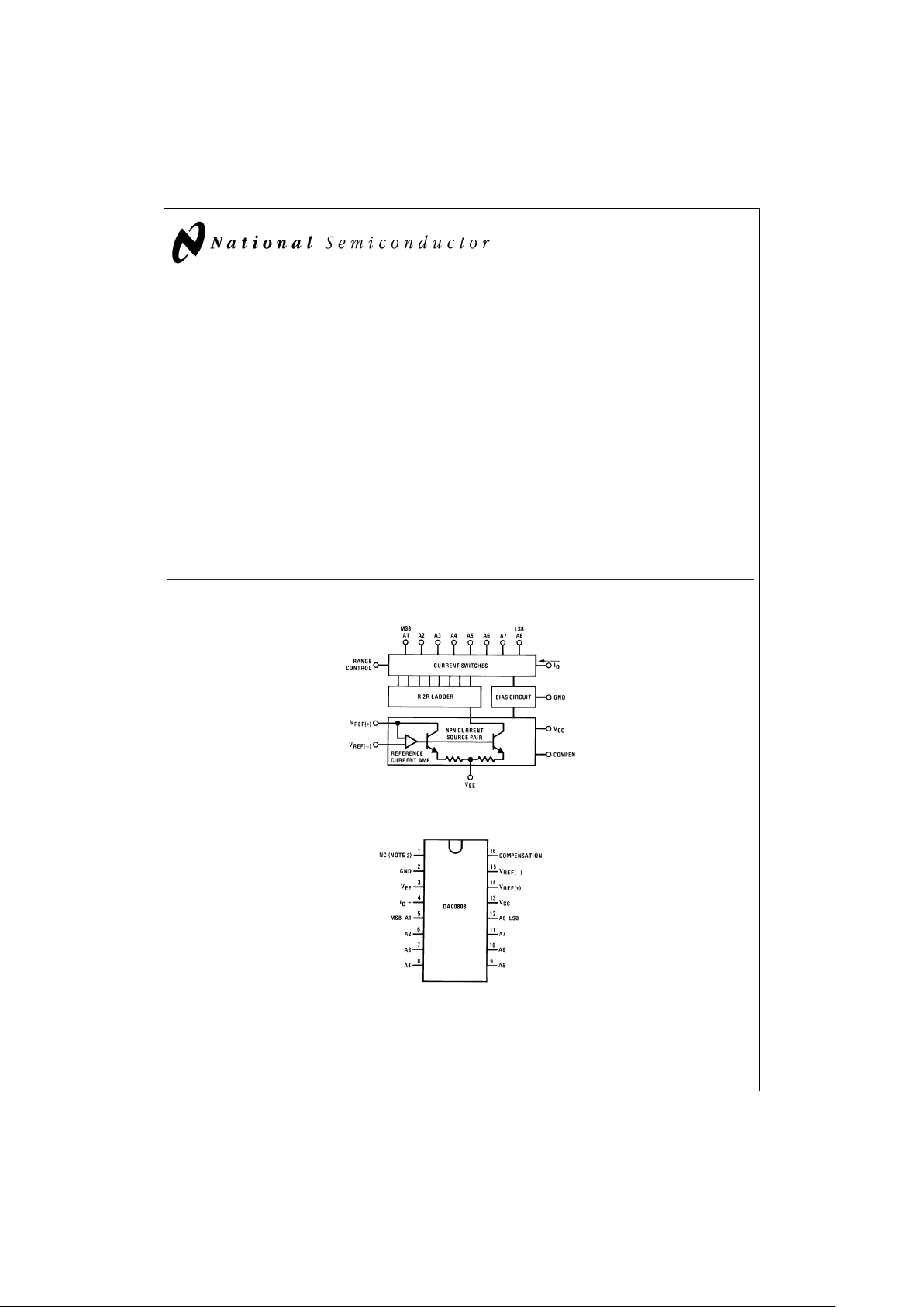
Block and Connection Diagrams
DS005687-1
Dual-In-Line Package
DS005687-2
Top View
Order Number DAC0808
See NS Package M16A or N16A
May 1999
DAC0808 8-Bit D/A Converter
© 1999 National Semiconductor Corporation DS005687 www.national.com
Page 2
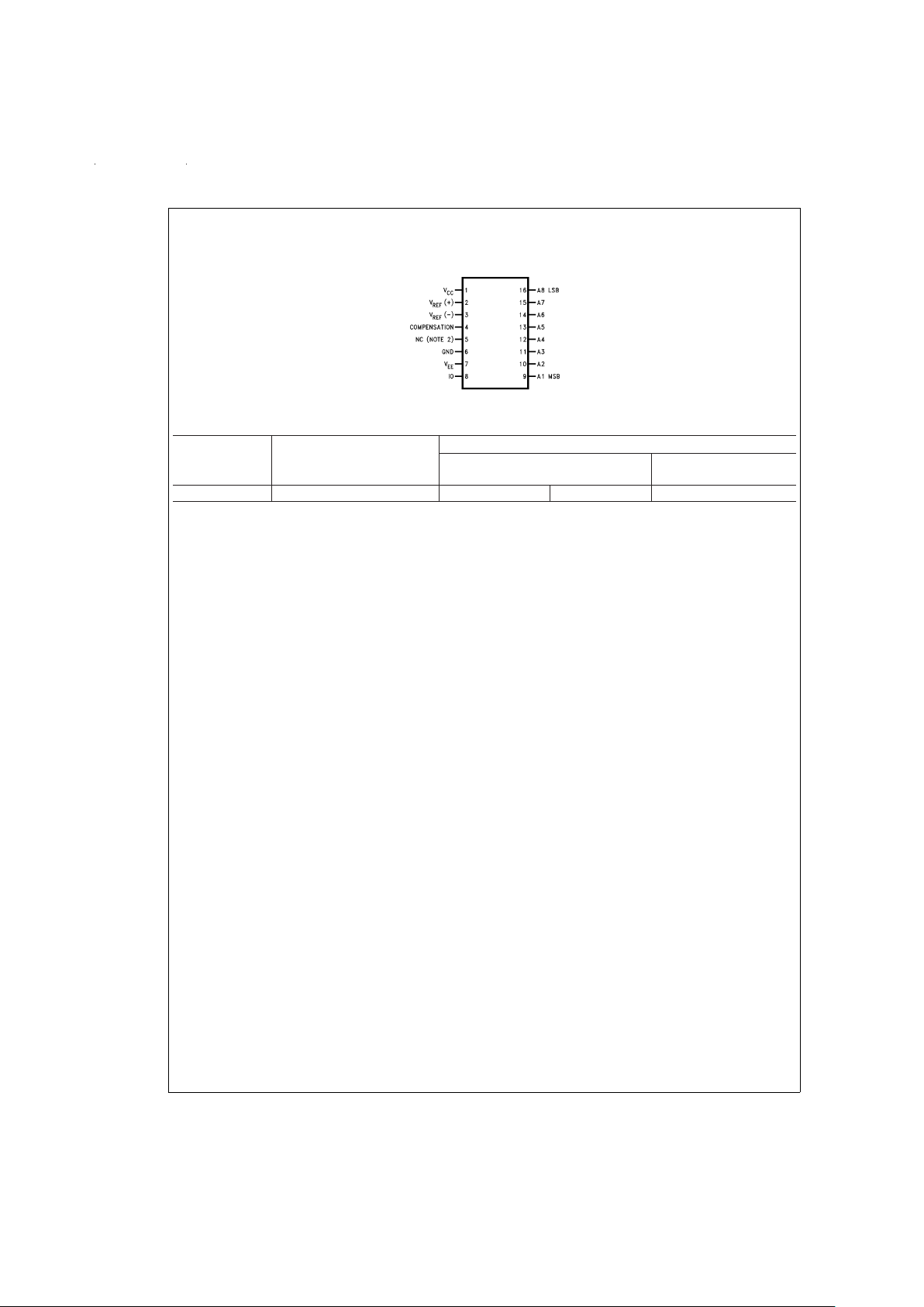
Block and Connection Diagrams (Continued)
Ordering Information
ACCURACY OPERATING
TEMPERATURE RANGE N PACKAGE (N16A)
(Note 1)
SO PACKAGE
(M16A)
8-bit 0˚C≤T
A
≤+75˚C DAC0808LCN MC1408P8 DAC0808LCM
Note 1: Devices may be ordered by using either order number.
Small-Outline Package
DS005687-13
www.national.com 2
Page 3

Absolute Maximum Ratings (Note 2)
If Military/Aerospace specified devices are required,
please contact the National Semiconductor Sales Office/
Distributors for availability and specifications.
Power Supply Voltage
V
CC
+18 V
DC
V
EE
−18 V
DC
Digital Input Voltage, V5–V12 −10 VDCto +18 V
DC
Applied Output Voltage, V
O
−11 VDCto +18 V
DC
Reference Current, I
14
5mA
Reference Amplifier Inputs, V14, V15 V
CC,VEE
Power Dissipation (Note 4) 1000 mW
ESD Susceptibility (Note 5) TBD
Storage Temperature Range −65˚C to +150˚C
Lead Temp. (Soldering, 10 seconds)
Dual-In-Line Package (Plastic) 260˚C
Dual-In-Line Package (Ceramic) 300˚C
Surface Mount Package
Vapor Phase (60 seconds) 215˚C
Infrared (15 seconds) 220˚C
Operating Ratings
Temperature Range T
MIN
≤ TA≤ T
MAX
DAC0808 0 ≤TA≤ +75˚C
Electrical Characteristics
(V
CC
=
5V, V
EE
=
−15 V
DC,VREF
/R14=2 mA, and all digital inputs at high logic level unless otherwise noted.)
Symbol Parameter Conditions Min Typ Max Units
E
r
Relative Accuracy (Error Relative (
Figure 4
)
%
to Full Scale I
O
)
DAC0808LC (LM1408-8)
±
0.19
%
Settling Time to Within
1
⁄2LSB T
A
=
25˚C (Note 7), 150 ns
(Includes t
PLH
)(
Figure 5
)
t
PLH,tPHL
Propagation Delay Time T
A
=
25˚C, (
Figure 5
) 30 100 ns
TCI
O
Output Full Scale Current Drift
±
20 ppm/˚C
MSB Digital Input Logic Levels (
Figure 3
)
V
IH
High Level, Logic “1” 2 V
DC
V
IL
Low Level, Logic “0” 0.8 V
DC
MSB Digital Input Current (
Figure 3
)
High Level V
IH
=
5V 0 0.040 mA
Low Level V
IL
=
0.8V −0.003 −0.8 mA
I
15
Reference Input Bias Current (
Figure 3
)−1−3µA
Output Current Range (
Figure 3
)
V
EE
=
−5V 0 2.0 2.1 mA
V
EE
=
−15V, T
A
=
25˚C 0 2.0 4.2 mA
I
O
Output Current V
REF
=
2.000V,
R14=1000Ω,
(
Figure 3
) 1.9 1.99 2.1 mA
Output Current, All Bits Low (
Figure 3
)04µA
Output Voltage Compliance (Note 3) E
r
≤ 0.19%,T
A
=
25˚C
V
EE
=
−5V, I
REF
=
1 mA −0.55, +0.4 V
DC
VEEBelow −10V −5.0, +0.4 V
DC
SRI
REF
Reference Current Slew Rate (
Figure 6
) 4 8 mA/µs
Output Current Power Supply −5V ≤ V
EE
≤ −16.5V 0.05 2.7 µA/V
Sensitivity
Power Supply Current (All Bits (
Figure 3
)
Low)
I
CC
2.3 22 mA
I
EE
−4.3 −13 mA
Power Supply Voltage Range T
A
=
25˚C, (
Figure 3
)
V
CC
4.5 5.0 5.5 V
DC
V
EE
−4.5 −15 −16.5 V
DC
Power Dissipation
www.national.com3
Page 4
Electrical Characteristics (Continued)
(V
CC
=
5V, V
EE
=
−15 V
DC,VREF
/R14=2 mA, and all digital inputs at high logic level unless otherwise noted.)
Symbol Parameter Conditions Min Typ Max Units
All Bits Low V
CC
=
5V, V
EE
=
−5V 33 170 mW
V
CC
=
5V, V
EE
=
−15V 106 305 mW
All Bits High V
CC
=
15V, V
EE
=
−5V 90 mW
V
CC
=
15V, V
EE
=
−15V 160 mW
Note 2: Absolute Maximum Ratings indicate limits beyond which damage to the device may occur. DC and AC electrical specifications do not apply when operating
the device beyond its specified operating conditions.
Note 3: Range control is not required.
Note 4: The maximum power dissipation must be derated at elevated temperatures and is dictated by T
JMAX
, θJA, and the ambient temperature, TA. The maximum
allowable power dissipation at any temperature is P
D
=
(T
JMAX−TA
)/θJAor the number given in the Absolute Maixmum Ratings, whichever is lower. For this device,
T
JMAX
=
125˚C, and the typical junction-to-ambient thermal resistance of the dual-in-line J package when the board mounted is 100˚C/W. For the dual-in-line N pack-
age, this number increases to 175˚C/W and for the small outline M package this number is 100˚C/W.
Note 5: Human body model, 100 pF discharged through a 1.5 kΩ resistor.
Note 6: All current switches are tested to guarantee at least 50%of rated current.
Note 7: All bits switched.
Note 8: Pin-out numbers for the DAL080X represent the dual-in-line package. The small outline package pinout differs from the dual-in-line package.
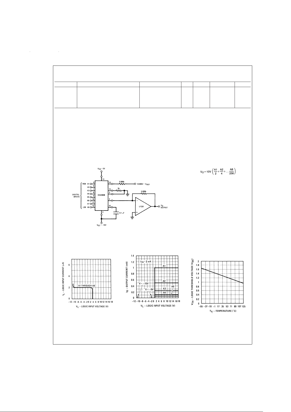
Typical Application
Typical Performance Characteristics
V
CC
=
5V, V
EE
=
−15V, T
A
=
25˚C, unless otherwise noted
DS005687-3
DS005687-23
FIGURE 1. +10V Output Digital to Analog Converter (Note 8)
Logic Input Current vs
Input Voltage
DS005687-14
Bit Transfer Characteristics
DS005687-15
Logic Threshold Voltage vs
Temperature
DS005687-16
www.national.com 4
Page 5
Typical Performance Characteristics V
CC
=
5V, V
EE
=
−15V, T
A
=
25˚C, unless otherwise
noted (Continued)
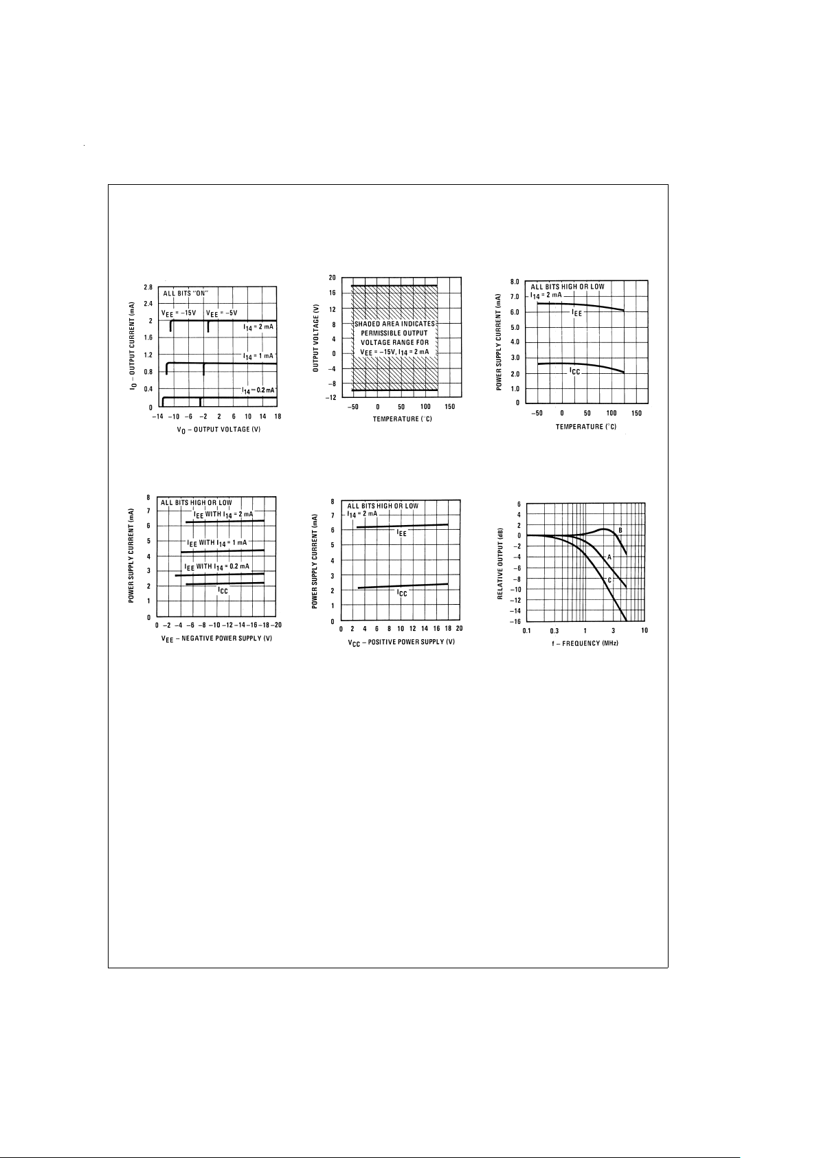
Unless otherwise specified: R14=R15=1kΩ,C=15 pF, pin 16 to V
EE;RL
=
50Ω, pin 4 to ground.
Curve A: Large Signal Bandwidth Method of
Figure 7
,V
REF
=
2 Vp-p offset 1V above ground.
Curve B: Small Signal Bandwidth Method of
Figure 7
,R
L
=
250Ω,V
REF
=
50 mVp-p offset 200 mV above ground.
Curve C: Large and Small Signal Bandwidth Method of
Figure 9
(no op amp, R
L
=
50Ω), R
S
=
50Ω,V
REF
=
2V,V
S
=
100 mVp-p
centered at 0V.
Output Current vs Output
Voltage (Output Voltage
Compliance)
DS005687-17
Output Voltage Compliance
vs Temperature
DS005687-18
Typical Power Supply
Current vs Temperature
DS005687-19
Typical Power Supply
Current vs V
EE
DS005687-20
Typical Power Supply
Current vs V
CC
DS005687-21
Reference Input
Frequency Response
DS005687-22
www.national.com5
Page 6
DS005687-4
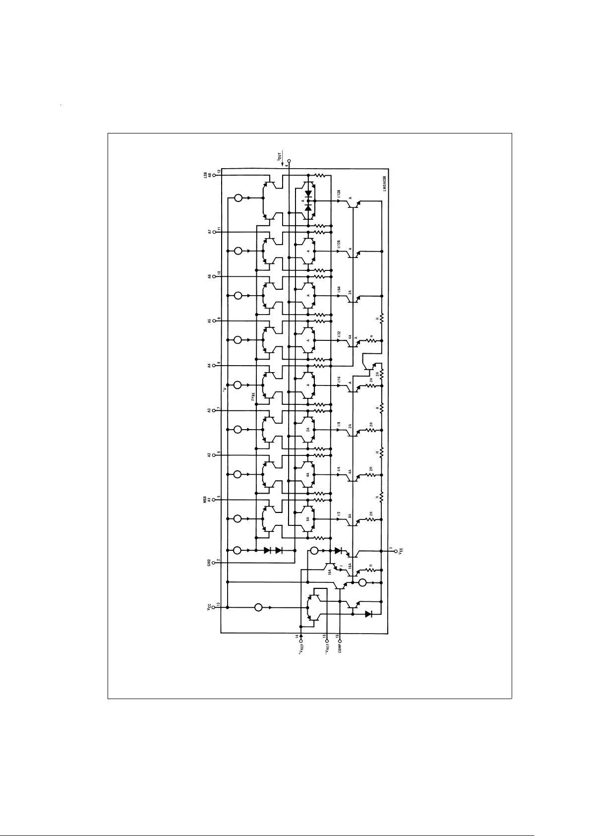
FIGURE 2. Equivalent Circuit of the DAC0808 Series (Note 8)
www.national.com 6
Page 7
Test Circuits
DS005687-6
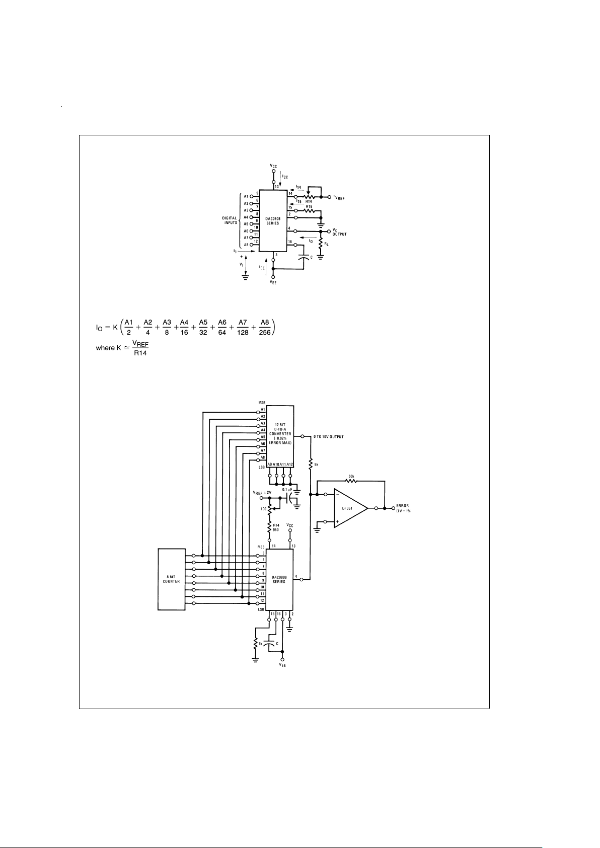
VIand I1apply to inputs A1–A8.
The resistor tied to pin 15 is to temperature compensate the bias current and may not be necessary for all applications.
and A
N
=
“1” if A
N
is at high level
A
N
=
“0” if A
N
is at low level
FIGURE 3. Notation Definitions Test Circuit (Note 8)
DS005687-7
FIGURE 4. Relative Accuracy Test Circuit (Note 8)
www.national.com7
Page 8
Test Circuits (Continued)
DS005687-8
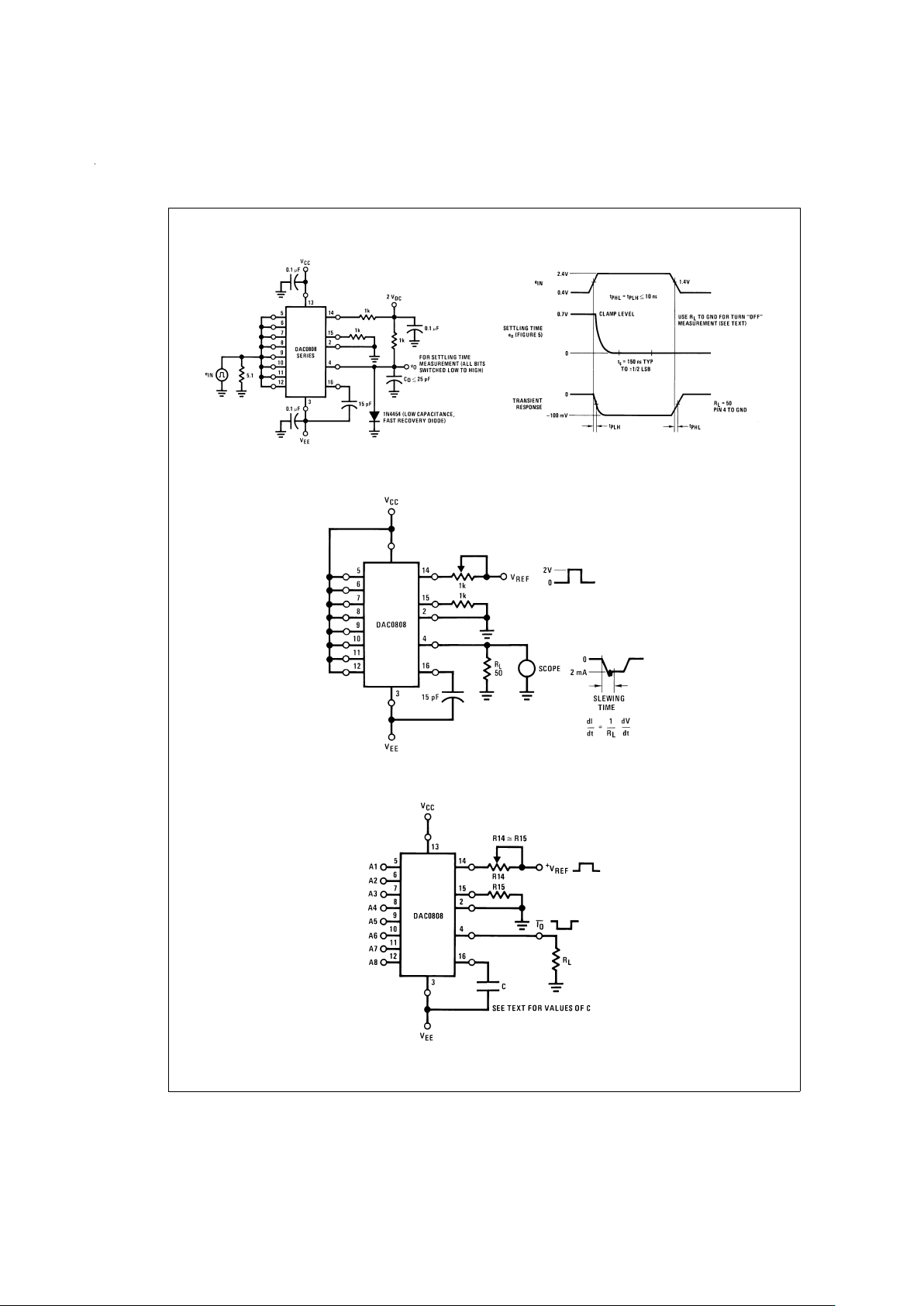
FIGURE 5. Transient Response and Settling Time (Note 8)
DS005687-9
FIGURE 6. Reference Current Slew Rate Measurement (Note 8)
DS005687-10
FIGURE 7. Positive V
REF
(Note 8)
www.national.com 8
Page 9
Test Circuits (Continued)
Application Hints
REFERENCE AMPLIFIER DRIVE AND COMPENSATION
The reference amplifier provides a voltage at pin 14 for converting the reference voltage to a current, and a turn-around
circuit or current mirror for feeding the ladder.The reference
amplifier input currrent, I
14
, must always flow into pin 14, re-
gardless of the set-up method or reference voltage polarity.
Connections for a positive voltage are shown in
Figure 7
.
The reference voltage source supplies the full current I
14
.
For bipolar reference signals, as in the multiplying mode,
R15 can be tied to a negative voltage corresponding to the
minimum input level. It is possible to eliminate R15 with only
a small sacrifice in accuracy and temperature drift.
The compensation capacitor value must be increased with
increases in R14 to maintain proper phase margin; for R14
values of 1, 2.5 and 5 kΩ, minimum capacitor values are 15,
37 and 75 pF. The capacitor may be tied to either V
EE
or
ground, but using V
EE
increases negative supply rejection.
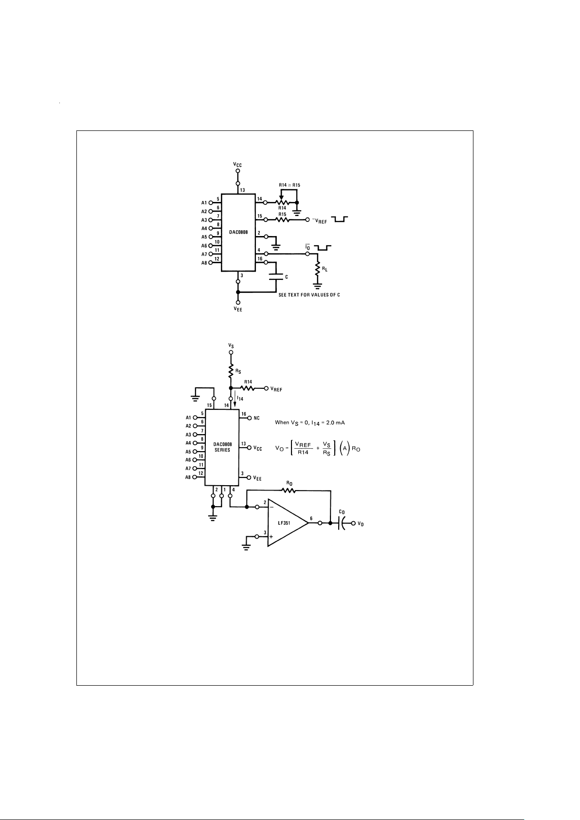
A negative reference voltage may be used if R14 is
grounded and the reference voltage is applied to R15 as
shown in
Figure 8
. A high input impedance is the main ad-
vantage of this method. Compensation involves a capacitor
DS005687-11
FIGURE 8. Negative V
REF
(Note 8)
DS005687-12
FIGURE 9. Programmable Gain Amplifier or
Digital Attenuator Circuit (Note 8)
www.national.com9
Page 10

Application Hints (Continued)
to V
EE
on pin 16, using the values of the previous paragraph.
The negative reference voltage must be at least 4V above
the V
EE
supply.Bipolar input signals may be handled by connecting R14 to a positive reference voltage equal to the peak
positive input level at pin 15.
When a DC reference voltage is used, capacitive bypass to
ground is recommended. The 5V logic supply is not recommended as a reference voltage. If a well regulated 5V supply
which drives logic is to be used as the reference, R14 should
be decoupled by connecting it to 5V through another resistor
and bypassing the junction of the 2 resistors with 0.1 µF to
ground. For reference voltages greater than 5V, a clamp diode is recommended between pin 14 and ground.
If pin 14 is driven by a high impedance such as a transistor
current source, none of the above compensation methods
apply and the amplifier must be heavily compensated, decreasing the overall bandwidth.
OUTPUT VOLTAGE RANGE
The voltage on pin 4 is restricted to a range of −0.55 to 0.4V
when V
EE
=
−5V due to the current switching methods em-
ployed in the DAC0808.
The negative output voltage compliance of the DAC0808 is
extended to −5V where the negative supply voltage is more
negative than −10V. Using a full-scale current of 1.992 mA
and load resistor of 2.5 kΩ between pin 4 and ground will
yield a voltage output of 256 levels between 0 and −4.980V.
Floating pin 1 does not affect the converter speed or power
dissipation. However, the value of the load resistor determines the switching time due to increased voltage swing.
Values of R
L
up to 500Ω do not significantly affect performance, but a 2.5 kΩ load increases worst-case settling time
to 1.2 µs (when all bits are switched ON). Refer to the subsequent text section on Settling Time for more details on output loading.
OUTPUT CURRENT RANGE
The output current maximum rating of 4.2 mA may be used
only for negative supply voltages more negative than −8V,
due to the increased voltage drop across the resistors in the
reference current amplifier.
ACCURACY
Absolute accuracy is the measure of each output current
level with respect to its intended value, and is dependent
upon relative accuracy and full-scale current drift. Relative
accuracy is the measure of each output current level as a
fraction of the full-scale current. The relative accuracy of the
DAC0808 is essentially constant with temperature due to the
excellent temperature tracking of the monolithic resistor lad-
der. The reference current may drift with temperature, causing a change in the absolute accuracy of output current.
However, the DAC0808 has a very low full-scale current drift
with temperature.
The DAC0808 series is guaranteed accurate to within
±
1
⁄
2
LSB at a full-scale output current of 1.992 mA. This corresponds to a reference amplifier output current drive to the
ladder network of 2 mA, with the loss of 1 LSB (8 µA) which
is the ladder remainder shunted to ground. The input current
to pin 14 has a guaranteed value of between 1.9 and 2.1 mA,
allowing some mismatch in the NPN current source pair.The
accuracy test circuit is shown in
Figure 4
. The 12-bit converter is calibrated for a full-scale output current of 1.992
mA. This is an optional step since the DAC0808 accuracy is
essentially the same between 1.5 and 2.5 mA. Then the
DAC0808 circuits’ full-scale current is trimmed to the same
value with R14 so that a zero value appears at the error amplifier output. The counter is activated and the error band
may be displayed on an oscilloscope, detected by comparators, or stored in a peak detector.
Two 8-bit D-to-A converters may not be used to construct a
16-bit accuracy D-to-A converter. 16-bit accuracy implies a
total error of
±
1
⁄2of one part in 65,536 or±0.00076%, which
is much more accurate than the
±
0.019%specification pro-
vided by the DAC0808.
MULTIPLYING ACCURACY
The DAC0808 may be used in the multiplying mode with
8-bit accuracy when the reference current is varied over a
range of 256:1. If the reference current in the multiplying
mode ranges from 16 µAto 4 mA, the additional error contributions are less than 1.6 µA. This is well within 8-bit accuracy when referred to full-scale.
A monotonic converter is one which supplies an increase in
current for each increment in the binary word. Typically, the
DAC0808 is monotonic for all values of reference current
above 0.5 mA. The recommended range for operation with a
DC reference current is 0.5 to 4 mA.
SETTLING TIME
The worst-case switching condition occurs when all bits are
switched ON, which corresponds to a low-to-high transition
for all bits. This time is typically 150 ns for settling to within
±
1
⁄2LSB, for 8-bit accuracy, and 100 ns to1⁄2LSB for 7 and
6-bit accuracy.The turn OFF is typically under 100 ns. These
times apply when R
L
≤ 500Ω and CO≤ 25 pF.
Extra care must be taken in board layout since this is usually
the dominant factor in satisfactory test results when measuring settling time. Short leads, 100 µF supply bypassing for
low frequencies, and minimum scope lead length are all
mandatory.
www.national.com 10
Page 11
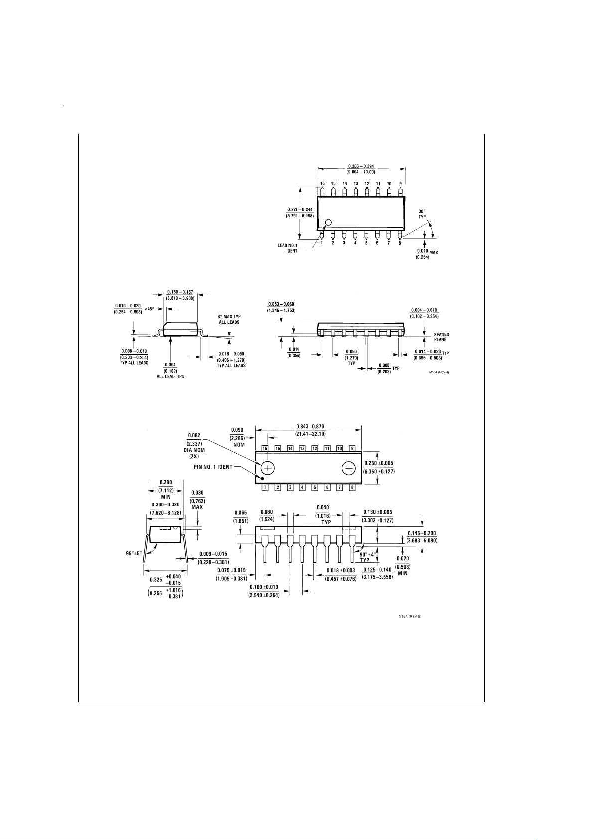
Physical Dimensions inches (millimeters) unless otherwise noted
Small Outline Package
Order Number DAC0808LCM
NS Package Number M16A
Dual-In-Line Package
Order Number DAC0808
NS Package Number N16A
www.national.com11
Page 12

Notes
LIFE SUPPORT POLICY
NATIONAL’S PRODUCTS ARE NOT AUTHORIZED FOR USE AS CRITICAL COMPONENTS IN LIFE SUPPORT
DEVICES OR SYSTEMS WITHOUT THE EXPRESS WRITTEN APPROVAL OF THE PRESIDENT AND GENERAL
COUNSEL OF NATIONAL SEMICONDUCTOR CORPORATION. As used herein:
1. Life support devices or systems are devices or
systems which, (a) are intended for surgical implant
into the body, or (b) support or sustain life, and
whose failure to perform when properly used in
accordance with instructions for use provided in the
labeling, can be reasonably expected to result in a
significant injury to the user.
2. A critical component is any component of a life
support device or system whose failure to perform
can be reasonably expected to cause the failure of
the life support device or system, or to affect its
safety or effectiveness.
National Semiconductor
Corporation
Americas
Tel: 1-800-272-9959
Fax: 1-800-737-7018
Email: [email protected]
National Semiconductor
Europe
Fax: +49 (0) 1 80-530 85 86
Email: [email protected]
Deutsch Tel: +49 (0) 1 80-530 85 85
English Tel: +49 (0) 1 80-532 78 32
Français Tel: +49 (0) 1 80-532 93 58
Italiano Tel: +49 (0) 1 80-534 16 80
National Semiconductor
Asia Pacific Customer
Response Group
Tel: 65-2544466
Fax: 65-2504466
Email: [email protected]
National Semiconductor
Japan Ltd.
Tel: 81-3-5639-7560
Fax: 81-3-5639-7507
www.national.com
DAC0808 8-Bit D/A Converter
National does not assume any responsibility for use of any circuitry described, no circuit patent licenses are implied and National reserves the right at any time without notice to change said circuitry and specifications.
 Loading...