

Page 1

E
PRELIMINARY
July 1998 Order Number: 290606-006
n
High-Density Symmetrically-Blocked
Architecture
64 128-Kbyte Erase Blocks (64 M)
32 128-Kbyte Erase Blocks (32 M)
n
4.5 V–5.5 V VCC Operation
2.7 V–3.6 V and 4.5 V–5.5 V I/O
Capable
n
Configurable x8 or x16 I/O
n
100 ns Read Access Time (32 M)
150 ns Read Access Time (64 M)
n
Enhanced Data Protection Features
Absolute Protection with
V
PEN
= GND
Flexible Block Locking
Block Erase/Program Lockout
during Power Transitions
n
Industry-Standard Packaging
µBGA* Package (64 M), SSOP and
TSOP Packages (32 M)
n
Cross-Compatible Command Support
Intel Basic Command Set
Common Flash Interface
Scaleable Command Set
n
32-Byte Write Buffer
6.3 µs per Byte Effective
Programming Time
n
6,400,000 Total Erase Cycles (64 M)
3,200,000 Total Erase Cycles (32 M)
100,000 Erase Cycles per Block
n
Automation Suspend Options
Block Erase Suspend to Read
Block Erase Suspend to Program
n
System Performance Enhancements
STS Status Output
n
Expanded Temperature Operation
–20 °C to +70 °C
n
Intel® StrataFlash™ Memory Flash
Technology
Capitalizing on two-bit-per-cell technol ogy, Intel® StrataFlash™ mem ory products provide 2X the bits in 1X
the space. Offered in 64-Mbit (8-Mbyte) and 32-Mbit (4-Mbyte) densities, Intel Strat aFlash memory devices
are the first to bring reliable, two-bit-per-cell storage technology to the flash market.
Intel StrataFlash memory benefits include: more density in less space, lowest cost-per-bit NOR devices,
support for code and data storage, and easy migration to future devices.
Using the same NOR-based ETOX™ technology as Intel’s one-bit-per-cell products, Intel StrataFlash
memory
devices take advantage of 400 million units of manufacturing experience since 1988. As a result,
Intel StrataFlash com ponents are ideal for code or data applications where high density and low cos t are
required. Examples include networking, telecommunications, audio recording, and digital imaging.
By applying FlashFile™ mem ory family pinouts, Intel StrataFlash mem ory components allow easy design
migrations from existing 28F016S A/SV, 28F032SA, and Word-W ide FlashFile memory devices (28F160S5
and 28F320S5).
Intel StrataFlash memory com ponents deliver a new generation of forward-compatible software support. By
using the Common Flash Interface (CFI) and the Scaleable Command Set (SCS), customers can take
advantage of density upgrades and optimized write capabilities of future Intel StrataFlash memory devices.
Manufactured on Intel’s 0.4 m icron ETOX™ V process technology, Int el StrataFlash memory provi des the
highest levels of quality and reliability.
INTEL® StrataFlash™ MEMORY TECHNOLOGY
32 AND 64 MBIT
28F320J5 and 28F640J5
Page 2

2
Information in this document is provided in connection with Intel products. No license, express or implied, by estoppel or
otherwise, to any intellectual property rights is granted by this document. Except as provided i n Intel’s Terms and Conditi ons of
Sale for such products, Intel assumes no liability whatsoever, and Intel disclaims any express or implied warranty, relating to
sale and/or use of Intel products including liability or warranties relating to fitness for a particular purpose, merchantability, or
infringement of any patent, copyright or other intellectual property right. Intel products are not intended for use in medical, life
saving, or life sustaining applications.
Intel may make changes to specifications and product descriptions at any time, without notice.
The 28F320J5 and 28F640J4 may contain design defects or errors known as errata. Current characterized errata are available
on request.
Contact your local Intel sales office or your distributor to obtain the latest specifications and before placing your product order.
Copies of documents which have an ordering number and are referenced in this document, or other Intel literature, may be
obtained from:
Intel Corporation
P.O. Box 5937
Denver, CO 8021-9808
or call 1-800-548-4725
or visit Intel’s website at http://www.intel.com
COPYRIGHT © INTEL CORPORATION 1997, 1998 CG-041493
*Third-party brands and names are the property of their respective owners.
Page 3

E INTEL
®
StrataFlash™ MEMORY TECHNOLOGY, 32 AND 64 MBIT
3
PRELIMINARY
CONTENTS
PAGE PAGE
1.0 PRODUCT OVERVIEW...................................5
2.0 PRINCIPLES OF OPERATION .....................11
2.1 Data Protection ..........................................12
3.0 BUS OPERATION.........................................12
3.1 Read..........................................................13
3.2 Output Disable...........................................13
3.3 Standby......................................................13
3.4 Reset/Power-Down....................................13
3.5 Read Query................................................14
3.6 Read Identifier Codes.................................14
3.7 Write ..........................................................14
4.0 COMMAND DEFINITIONS............................14
4.1 Read Array Command................................18
4.2 Read Query Mode Command.....................18
4.2.1 Query Structure Output .......................18
4.2.2 Query Structure Overview ...................20
4.2.3 Block Status Register..........................21
4.2.4 CFI Query Identification String.............22
4.2.5 System Interface Information...............23
4.2.6 Device Geometry Definition.................24
4.2.7 Primary-Vendor Specific Extended
Query Table .......................................25
4.3 Read Identifier Codes Command...............26
4.4 Read Status Register Command................27
4.5 Clear Status Register Command................27
4.6 Block Erase Command ..............................27
4.7 Block Erase Suspend Command................27
4.8 Write to Buffer Command...........................28
4.9 Byte/Word Program Commands.................28
4.10 Configuration Command...........................29
4.11 Set Block and Master Lock-Bit
Commands................................................29
4.12 Clear Block Lock-Bits Command..............30
5.0 DESIGN CONSIDERATIONS........................40
5.1 Three-Line Output Control..........................40
5.2 STS and Block Erase, Program, and Lock-
Bit Configuration Polling............................40
5.3 Power Supply Decoupling ..........................40
5.4 V
CC
, V
PEN
, RP# Transitions........................40
5.5 Power-Up/Down Protection........................41
5.6 Power Dissipation.......................................41
6.0 ELECTRICAL SPECIFICATIONS..................42
6.1 Absolute Maximum Ratings........................42
6.2 Operating Conditions..................................42
6.3 Capacitance...............................................42
6.4 DC Characteristics .....................................43
6.5 AC Characteristics—Read-Only
Operations.................................................46
6.6 AC Characteristics— Write Operations.......48
6.7 Block Erase, Program, and Lock-Bit
Configuration Performance........................51
7.0 ORDERING INFORMATION..........................52
8.0 ADDITIONAL INFORMATION.......................53
Page 4
INTEL
®
StrataFlash™ MEMORY TECHNOLOGY, 32 AND 64 MBIT E
4
PRELIMINARY
REVISION HISTORY
Date of
Revision
Version Description
09/01/97 -001 Original Version
09/17/97 -002 Modifications made to cover sheet
12/01/97 -003 VCC/GND Pins Converted to No Connects specification change added
I
CCS
, I
CCD
, I
CCW
, and I
CCE
specification change added
Order Codes specification change added
1/31/98 -004 The µBGA* chip-scale package in Figure 2 was changed to a 52-ball
package and appropriate documentation added. The 64-Mb µBGA
package dimensions were changed in Figure 2. Changed Figure 4 to read
SSOP instead of TSOP.
3/23/98 -005 32-Mbit Intel StrataFlash memory read access time added. The number
of block erase cycles was changed. The write buffer program time was
changed. The operating temperature was changed. A read parameter
was added. Several program, erase, and lock-bit specifications were
changed. Minor documentation changes were made as well. Datasheet
designation changed from Advance Information to Preliminary.
7/13/98 -006 Intel StrataFlash memory 32-Mb µBGA package removed. t
EHEL
read
specification reduced. Table 4 was modified. The
Ordering Information
was updated.
Page 5

E INTEL
®
StrataFlash™ MEMORY TECHNOLOGY, 32 AND 64 MBIT
5
PRELIMINARY
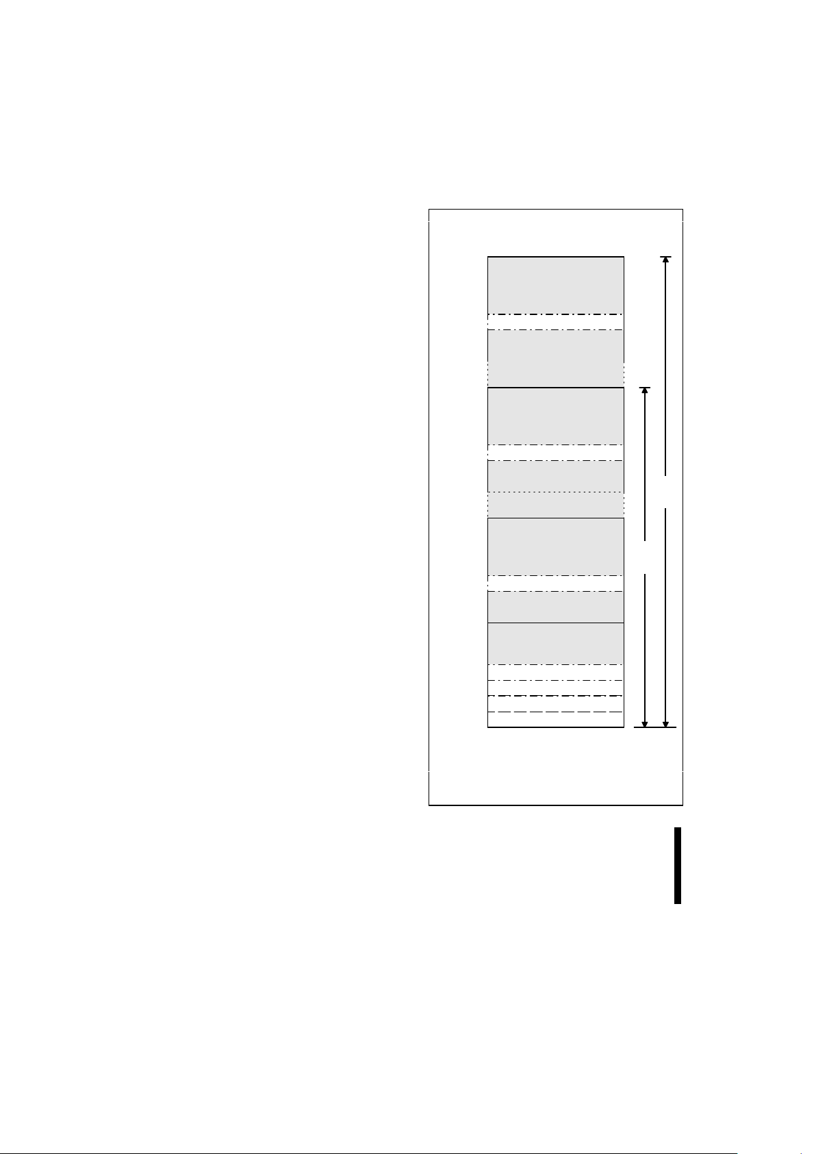
1.0 PRODUCT OVERVIEW
The Intel® StrataFlash™ memory famil y contains
high-density memories organiz ed as 8 Mbytes or
4 Mwords (64-Mbit) and 4 Mbytes or 2 Mwords
(32-Mbit). These devices can be accessed as 8- or
16-bit words. The 64-Mbit devic e is organized as
sixty-four 128-Kbyt e (131,072 bytes) erase block s
while the 32-Mbits device c ontains thirty-two 128Kbyte erase blocks. Blocks are selectively and
individually lockable and unlockable in-system.
See the memory map in Figure 5.
A Common Flash Interface (CFI) permits software
algorithms to be used for entire families of
devices. This allows device-independent, JEDEC
ID-independent, and forward- and backwardcompatible software support for the s pecified fl ash
device families. Flash vendors can standardize
their existing interfaces for long-term compatibility.
Scaleable Command Set (SCS) allows a single,
simple software driver in all host systems to work
with all SCS-compliant flash memory devices,
independent of system-level packaging (e.g.,
memory card, SIMM, or direct-to-board placement). Additionally, SCS provides the highest
system/device data transfer rates and minimizes
device and system-level implementation costs.
A Command User Interface (CUI) serves as the
interface between the system processor and
internal operation of the device. A valid c ommand
sequence written to the CUI initiates device
automation. An internal Write State Machine
(WSM) automatically ex ecutes the algorithms and
timings necessary for block erase, program, and
lock-bit configuration operations.
A block erase operation erases one of the devic e’s
128-Kbyte blocks typically within one second—
independent of other blocks. Each block can be
independently erased 100,000 times . Block erase
suspend mode allows system software to suspend
block erase to read or program data from any
other block.
Each device incorporates a Write Buffer of
32 bytes (16 words) to allow optimum
programming performance. By using the Write
Buffer, data is programmed in buffer increments.
This feature can improve system program
performance by up to 20 times over non Write
Buffer writes.
Individual block locking us es a combi nation of bit s,
block lock-bits and a m aster lock-bit, to lock and
unlock blocks. Block lock-bits gate block erase
and program operations while the master l ock-bit
gates block lock-bit modification. Three lock-bit
configuration operations set and clear lock-bits
(Set Block Lock-Bit, Set Master Lock-Bit, and
Clear Block Lock-Bits commands).
The status register indicates when the WSM’s
block erase, program, or lock-bit configuration
operation is finished.
The STS (STATUS) output gives an additional
indicator of WSM activity by providing both a
hardware signal of status (vers us software polling)
and status masking (interrupt masking for
background block erase, for example). Status
indication using STS minimizes both CPU
overhead and system power consumption. When
configured in level mode (default mode), it acts as
a RY/BY# pin. When low, STS indicat es that the
WSM is performing a block erase, program, or
lock-bit configuration. S TS-high indicates that the
WSM is ready for a new command, block erase is
suspended (and programming is inactive), or the
device is in reset/power-down m ode. Additionally,
the configuration command all ows the STS pin to
be configured to pulse on completion of
programming and/or block erases.
Three CE pins are used to enable and disable the
device. A unique CE logic design (see Table 2,
Chip Enable Truth Table
) reduces decoder logic
typically required for multi-chip designs. External
logic is not required when designing a s ingle chip,
a dual chip, or a 4-chip miniature card or SIMM
module.
The BYTE# pin allows either x8 or x16 read/writes
to the device. BYTE# at logic low selects 8-bit
mode; address A
0
selects between the low byte
and high byte. BYTE# at logic hi gh enables 16-bit
operation; address A
1
becomes the lowest order
address and address A
0
is not used (don’t care). A
device block diagram is shown in Figure 1.
When the device is disabled (see Table 2,
Chip
Enable Truth Table
) and the RP# pin is at VCC, the
standby mode is enabled. When the RP # pin is at
GND, a further power-down mode is enabled
which minimizes power consumpti on and provides
write protection during reset. A res et time (t
PHQV
)
is required from RP# switchi ng high until outputs
Page 6
INTEL
®
StrataFlash™ MEMORY TECHNOLOGY, 32 AND 64 MBIT E
6
PRELIMINARY
are valid. Likewise, the device has a wake time
(t
PHWL
) from RP#-high until writes to t he CUI are
recognized. With RP# at GND, the WSM is reset
and the status register is cleared.
The Intel StrataFlash memory devices are
available in several package t ypes. The 64-Mbit is
available in 56-lead SSOP (Shrink Small Outline
Package) and µBGA* package (micro Ball Grid
Array). The 32-Mbit is availabl e in 56-lead TSOP
(Thin Small Outline Package) and 56-lead SSOP.
Figures 2, 3, and 4 show the pinouts.
32-Mbit: Thirty-two
64-Mbit: Sixty-four
128-Kbyte Blocks
Input Buffer
Output
Multiplexer
Y-Gating
Program/Erase
Voltage Switch
Data
Comparator
Status
Register
Identifier
Register
Data
Register
I/O Logic
Address
Latch
Address
Counter
X-Decoder
Y-Decoder
Input Buffer
Output Buffer
GND
V
CC
V
PEN
CE
0
CE
1
CE
2
WE#
OE#
RP#
BYTE#
Command
User
Interface
32-Mbit: A0- A
21
64-Mbit: A
0 - A22
DQ0 - DQ
15
V
CC
Write Buffer
Write State
Machine
Multiplexer
Query
STS
V
CCQ
CE
Logic
0606_01
Figure 1. Intel® StrataFlash™ Memory Block Diagram
Page 7
E INTEL
®
StrataFlash™ MEMORY TECHNOLOGY, 32 AND 64 MBIT
7
PRELIMINARY
Table 1. Lead Descriptions
Symbol Type Name and Function
A
0
INPUT BYTE-SELECT ADDRESS: Selects between high and low byte when the device
is in x8 mode. This address is latched during a x8 program cycle. Not used in
x16 mode (i.e., the A
0
input buffer is turned off when BYTE# is high).
A1–A
22
INPUT ADDRESS INPUTS: Inputs for addresses during read and program operations.
Addresses are internally latched during a program cycle.
32-Mbit: A
0–A21
64-Mbit: A0–A
22
DQ0–DQ
7
INPUT/
OUTPUT
LOW-BYTE DATA BUS: Inputs data during buffer writes and programming, and
inputs commands during Command User Interface (CUI) writes. Outputs array,
query, identifier, or status data in the appropriate read mode. Floated when the
chip is de-selected or the outputs are disabled. Outputs DQ
6
–DQ0 are also
floated when the Write State Machine (WSM) is busy. Check SR.7 (Status
Register bit 7) to determine WSM status.
DQ8–DQ
15
INPUT/
OUTPUT
HIGH-BYTE DATA BUS: Inputs data during x16 buffer writes and programming
operations. Outputs array, query, or identifier data in the appropriate read mode;
not used for Status Register reads. Floated when the chip is de-selected, the
outputs are disabled, or the WSM is busy.
CE0,
CE
1
,
CE
2
INPUT CHIP ENABLES: Activates the device’s control logic, input buffers, decoders,
and sense amplifiers. When the device is de-selected (see Table 2,
Chip Enable
Truth Table
), power reduces to standby levels.
All timing specifications are the same for these three signals. Device selection
occurs with the first edge of CE
0
, CE1, or CE2 that enables the device. Device
deselection occurs with the first edge of CE
0
, CE1, or CE2 that disables the
device (see Table 2,
Chip Enable Truth Table
).
RP# INPUT RESET/ POWER-DOWN: Resets internal automation and puts the device in
power-down mode. RP#-high enables normal operation. Exit from reset sets the
device to read array mode. When driven low, RP# inhibits write operations which
provides data protection during power transitions.
RP# at V
HH
enables master lock-bit setting and block lock-bits configuration
when the master lock-bit is set. RP# = V
HH
overrides block lock-bits thereby
enabling block erase and programming operations to locked memory blocks. Do
not permanently connect RP# to V
HH
.
OE# INPUT OUTPUT ENABLE: Activates the device’s outputs through the data buffers
during a read cycle. OE# is active low.
WE# INPUT WRITE ENABLE: Controls writes to the Command User Interface, the Write
Buffer, and array blocks. WE# is active low. Addresses and data are latched on
the rising edge of the WE# pulse.
STS OPEN
DRAIN
OUTPUT
STATUS: Indicates the status of the internal state machine. When configured in
level mode (default mode), it acts as a RY/BY# pin. When configured in one of
its pulse modes, it can pulse to indicate program and/or erase completion. For
alternate configurations of the STATUS pin, see the Configurations command.
Tie STS to V
CCQ
with a pull-up resistor.
Page 8
INTEL
®
StrataFlash™ MEMORY TECHNOLOGY, 32 AND 64 MBIT E
8
PRELIMINARY
Table 1. Lead Descriptions (Continued)
Symbol Type Name and Function
BYTE# INPUT BYTE ENABLE: BYTE# low places the device in x8 mode. All data is then input
or output on DQ
0
–DQ7, while DQ8–DQ15 float. Address A0 selects between the
high and low byte. BYTE# high places the device in x16 mode, and turns off the
A
0
input buffer. Address A1 then becomes the lowest order address.
V
PEN
INPUT ERASE / PROGRAM / BLOCK LOCK ENABLE: For erasing array blocks,
programming data, or configuring lock-bits.
With V
PEN
≤ V
PENLK
, memory contents cannot be altered.
V
CC
SUPPLY DEVICE POWER SUPPLY: With VCC ≤ V
LKO
, all write attempts to the flash
memory are inhibited.
V
CCQ
OUTPUT
BUFFER
SUPPLY
OUTPUT BUFFER POWER SUPPLY: This voltage controls the device’s output
voltages. To obtain output voltages compatible with system data bus voltages,
connect V
CCQ
to the system supply voltage.
GND SUPPLY GROUND: Do not float any ground pins.
NC NO CONNECT: Lead is not internally connected; it may be driven or floated.
Page 9
E INTEL
®
StrataFlash™ MEMORY TECHNOLOGY, 32 AND 64 MBIT
9
PRELIMINARY
GND A10V
PENCE0A14VCC
A7A9A11A12A15A
17
A
4
A
19
A6A8RP# A13A16A
21
A
5
A
20
A1A
3
A18CE
1
A
2
A
22
BYTE# DQ
7
CE
2
WE#
DQ8DQ
1
DQ6DQ
15
A
0
OE#DQ3DQ
12
DQ9DQ
2
DQ13DQ
14
DQ
0
STSDQ11DQ
4
V
CC
(1)
DQ
10
DQ5GND
(1)
GND V
CCQ
GNDA
10
V
PEN
CE
0
A
14
V
CC
A
7
A
9
A
11
A
12
A
15
A
17
A
4
A
19
A
6
A
8
RP#A
13
A
16
A
21
A
5
A
20
A
1
A
3
A
18
CE
1
A
2
A
22
BYTE#DQ
7
CE
2
WE#
DQ
8
DQ
1
DQ
6
DQ
15
A
0
OE# DQ
3
DQ
12
DQ
9
DQ
2
DQ
13
DQ
14
DQ
0
STS DQ
11
DQ
4
V
CC
(1)
DQ
10
DQ
5
GND
(1)
GNDV
CCQ
A
B
C
D
E
F
G
H
I
A
B
C
D
E
F
G
H
I
78 6543
21
21 3456
78
Top ViewBottom View - Ball Side Up
NC
(1)
NC
(1)
NC
(1)
NC
(1)
64-Mbit Intel® StrataFlash™ Memory: 7.67 mm x 16.37 mm
NOTE:
1. VCC (Ball I7), GND (Ball I2), and NC (Balls F2 and F7) have been removed. Future generations of Intel StrataFlash
memory may make use of these missing ball locations.
Figures are not drawn to scale.
Figure 2. µBGA* Package (64 Mbit)
Page 10
INTEL
®
StrataFlash™ MEMORY TECHNOLOGY, 32 AND 64 MBIT E
10
PRELIMINARY
28F320J5
Intel® StrataFlash™ Memory
56-Lead TSOP
Standard Pinout
14 mm x 20 mm
Top View
1
3
4
2
5
7
8
6
9
11
12
10
13
15
16
14
17
19
20
18
21
23
24
22
25
27
28
26
56
54
53
55
52
50
49
51
48
46
45
47
44
42
41
43
40
38
37
39
36
34
33
35
32
30
29
31
NC
A
21
A
20
CE
1
A
19
A
17
A
16
A
18
V
CC
A
14
A
13
A
15
A
12
V
PEN
RP#
CE
0
A
11
A
9
A
8
A
10
GND
A
6
A
5
A
7
A
4
A
2
A
1
A
3
28F016SV
28F016SA
28F032SA
3/5#
NC
A
20
CE
1
A
19
A
17
A
16
A
18
V
CC
A
14
A
13
A
15
A
12
V
PP
RP#
CE
0
A
11
A
9
A
8
A
10
GND
A
6
A
5
A
7
A
4
A
2
A
1
A
3
3/5#
CE
2
A
20
CE
1
A
19
A
17
A
16
A
18
V
CC
A
14
A
13
A
15
A
12
V
PP
RP#
CE
0
A
11
A
9
A
8
A
10
Highlights pinout changes
A
6
A
5
A
7
A
4
A
2
A
1
A
3
GND
28F160S5
NC
NC
A
20
CE
1
A
19
A
17
A
16
A
18
V
CC
A
14
A
13
A
15
A
12
V
PP
RP#
CE
0
A
11
A
9
A
8
A
10
A
6
A
5
A
7
A
4
A
2
A
1
A
3
GND
NC
OE#
STS
WE#
DQ
15
DQ
14
DQ
6
DQ
7
GND
DQ
5
DQ
12
DQ
13
DQ
4
GND
DQ
11
V
CCQ
DQ
3
DQ
2
V
CC
DQ
10
DQ
9
DQ
8
DQ
0
DQ
1
A
0
NC
CE
2
BYTE#
28F016SV
28F016SA
28F032SA
WP#
OE#
RY/BY#
WE#
DQ
15
DQ
14
DQ
6
DQ
7
GND
DQ
5
DQ
12
DQ
13
GND
DQ
11
DQ
3
DQ
2
V
CC
DQ
10
DQ
9
DQ
8
DQ
0
DQ
1
A
0
NC
NC
BYTE#
WP#
OE#
RY/BY#
WE#
DQ
15
DQ
14
DQ
6
DQ
7
GND
DQ
5
DQ
12
DQ
13
DQ
11
DQ
3
DQ
2
V
CC
DQ
10
DQ
9
DQ
8
DQ
0
DQ
1
A
0
NC
NC
BYTE#
28F320J5 28F160S5
WP#
OE#
STS
WE#
DQ
15
DQ
14
DQ
6
DQ
7
GND
DQ
5
DQ
12
DQ
13
GND
DQ
11
DQ
3
DQ
2
V
CC
DQ
10
DQ
9
DQ
8
DQ
0
DQ
1
A
0
NC
NC
BYTE#
V
CC
DQ
4
GND
V
CCVCC
DQ4DQ
4
0606_03
NOTE:
1. VCC (Pin 37) and GND (Pin 48) are not internally connected. For future device revisions, it is recommended that these
pins be connected to their respected power supplies (i.e., Pin 37 = VCC and Pin 48 = GND).
2. For compatibility with future generations of Intel® StrataFlash™ memory, this NC (pin 56) should be connected to GND.
Figure 3. TSOP Lead Configuration (32 Mbit)
Page 11
E INTEL
®
StrataFlash™ MEMORY TECHNOLOGY, 32 AND 64 MBIT
11
PRELIMINARY
Intel
®
StrataFlash™ Memory
56-Lead SSOP
Standard Pinout
16 mm x 23.7 mm
Top View
1
3
4
2
5
7
8
6
9
11
12
10
13
15
16
14
17
19
20
18
21
23
24
22
25
27
28
26
56
54
53
55
52
50
49
51
48
46
45
47
44
42
41
43
40
38
37
39
36
34
33
35
32
30
29
31
V
PEN
A
11
A
10
RP#
A
9
A
2
A
3
A
1
A
4
A
6
A
7
A
5
GND
V
CC
DQ
9
A
8
DQ
1
DQ
0
A
0
DQ
8
BYTE#
CE
2
DQ
2
NC
DQ
10
DQ
11
GND
DQ
3
V
PEN
A
11
A
10
RP#
A
9
A
2
A
3
A
1
A
4
A
6
A
7
A
5
GND
V
CC
DQ
9
A
8
DQ
1
DQ
0
A
0
DQ
8
BYTE#
CE
2
DQ
2
NC
DQ
10
DQ
11
GND
DQ
3
V
PP
A
11
A
10
RP#
A
9
A
2
A
3
A
1
A
4
A
6
A
7
A
5
GND
V
CC
DQ
9
A
8
DQ
1
DQ
0
A
0
DQ
8
BYTE#
NC
DQ
2
NC
DQ
10
DQ
11
GND
DQ
3
28F640J5 28F320J5 28F320S528F640J528F320J5
Highlights pinout changes.
28F320S5
RY/BY#
28F160S5
28F016SV
28F016SA
CE
0
A
13
A
14
A
12
A
15
CE
1
A
21
NC
A
20
A
18
A
17
A
19
A
16
DQ
6
V
CC
DQ
14
DQ
15
STS
DQ
7
OE#
NC
DQ
13
WE#
DQ
5
DQ
4
V
CCQ
DQ
12
GND
CE
0
A
13
A
14
A
12
A
15
CE
1
A
21
A
20
A
18
A
17
A
19
A
16
DQ
6
V
CC
DQ
14
DQ
15
STS
DQ
7
OE#
NC
DQ
13
WE#
DQ
5
DQ
4
V
CCQ
DQ
12
A
22
GND
CE0#
A
13
A
14
A
12
A
15
CE1#
NC
A
20
A
18
A
17
A
19
A
16
GND
DQ
6
V
CC
DQ
14
DQ
15
RY/BY#
DQ
7
OE#
WP#
DQ
13
WE#
DQ
5
DQ
4
V
CC
DQ
12
A
21
CE0#
A
13
A
14
A
12
A
15
CE1#
NC
A
20
A
18
A
17
A
19
A
16
GND
DQ
6
V
CC
DQ
14
DQ
15
DQ
7
OE#
WP#
DQ
13
WE#
DQ
5
DQ
4
V
CC
DQ
12
NC
CE0#
A
13
A
14
A
12
A
15
CE1#
3/5#
A
20
A
18
A
17
A
19
A
16
GND
DQ
6
V
CC
DQ
14
DQ
15
RY/BY#
DQ
7
OE#
WP#
DQ
13
WE#
DQ
5
DQ
4
V
CC
DQ
12
NC
V
PP
A
11
A
10
RP#
A
9
A
2
A
3
A
1
A
4
A
6
A
7
A
5
GND
V
CC
DQ
9
A
8
DQ
1
DQ
0
A
0
DQ
8
BYTE#
NC
DQ
2
NC
DQ
10
DQ
11
GND
DQ
3
28F160S5
V
PP
A
11
A
10
RP#
A
9
A
2
A
3
A
1
A
4
A
6
A
7
A
5
GND
V
CC
DQ
9
A
8
DQ
1
DQ
0
A
0
DQ
8
BYTE#
NC
DQ
2
NC
DQ
10
DQ
11
GND
DQ
3
28F016SV
28F016SA
0606_04
NOTE:
1. VCC (Pin 42) and GND (Pin 15) are not internally connected. For future device revisions, it is recommended that these
pins be connected to their respected power supplies (i.e., Pin 42 = VCC and Pin 15 = GND).
2. For compatibility with future generations of Intel StrataFlash memory, this NC (pin 23) should be connected to GND
Figure 4. SSOP Lead Configuration (64 Mbit and 32 Mbit)
2.0 PRINCIPLES OF OPERATION
The Intel StrataFlash memory devices include an
on-chip WSM to manage block eras e, program, and
lock-bit configuration functions. It allows for 100%
TTL-level control inputs, fixed power supplies
during block erasure, program, lock-bit
configuration, and minimal process or overhead with
RAM-like interface timings.
After initial device power-up or return from
reset/power-down mode (see Bus Operations), the
device defaults to read array mode. Manipul ation of
external memory control pins allows array read,
standby, and output disable operations.
Read array, status register, query, and identifier
codes can be accessed through the CUI (Command
User Interface) independent of the V
PEN
voltage.
Page 12
INTEL
®
StrataFlash™ MEMORY TECHNOLOGY, 32 AND 64 MBIT E
12
PRELIMINARY
V
PENH
on V
PEN
enables successful block erasure,
programming, and lock-bit configuration. All
functions associated with altering memory
contents—block erase, program, lock-bit
configuration—are accessed via the CUI and
verified through the status register.
Commands are written using standard microprocessor write timings . The CUI cont ents s erve as
input to the WSM, which c ontrols the block erase,
program, and lock-bit configuration. The internal
algorithms are regulated by the WSM, including
pulse repetition, internal v erification, and margini ng
of data. Addresses and data are internally lat ched
during program cycles.
Interface software that initiates and polls progress
of block erase, program, and lock-bit configuration
can be stored in any block. This code is c opied to
and executed from system RAM during flash
memory updates. After successful completion,
reads are again possible via the Read Array
command. Block erase suspend allows system
software to suspend a block erase to read or
program data from/to any other block.
2.1 Data Protection
Depending on the application, the system designer
may choose to make the V
PEN
switchable (availabl e
only when memory block erases , program s, or loc kbit configurations are required) or hardwired to
V
PENH
. The device accommodates either design
practice and encourages optimization of the
processor-memory interface.
When V
PEN
≤ V
PENLK
, memory contents c annot be
altered. The CUI’s two-step block erase, byte/word
program, and lock-bit configuration command
sequences provide protection from unwanted
operations even when V
PENH
is applied to V
PEN
. All
program functions are disabled when V
CC
is below
the write lockout v oltage V
LKO
or when RP# is VIL.
The device’s block locking capability provides
additional protection from inadv ertent code or data
alteration by gating erase and program operations.
3.0 BUS OPERATION
The local CPU reads and writes flash memory
in-system. All bus cycles to or from the flash
memory conform to standard microprocessor bus
cycles.
64-Kword Block
64-Kword Block
64-Kword Block
64-Kword Block
31
1
0
63
Word Wide (x16) Mode
1FFFFF
1F0000
3FFFFF
3F0000
01FFFF
010000
00FFFF
000000
A [22-1]: 64-Mbit
A [21-1]: 32-Mbit
128-Kbyte Block
128-Kbyte Block
128-Kbyte Block
128-Kbyte Block
31
1
0
63
Byte-Wide (x8) Mode
3FFFFF
3E0000
7FFFFF
7E0000
03FFFF
020000
01FFFF
000000
A [22-0]: 64-Mbit
A [21-0]: 32-Mbit
32-Mbit
64-Mbit
0606_05
Figure 5. Memory Map
Page 13

E INTEL
®
StrataFlash™ MEMORY TECHNOLOGY, 32 AND 64 MBIT
13
PRELIMINARY
Table 2. Chip Enable Truth Table
(1,2)
CE
2
CE
1
CE
0
DEVICE
V
IL
V
IL
V
IL
Enabled
V
IL
V
IL
V
IH
Disabled
V
IL
V
IH
V
IL
Disabled
V
IL
V
IH
V
IH
Disabled
V
IH
V
IL
V
IL
Enabled
V
IH
V
IL
V
IH
Enabled
V
IH
V
IH
V
IL
Enabled
V
IH
V
IH
V
IH
Disabled
NOTE:
1. See Application Note
AP-647 Intel StrataFlash™
Memory Design Guide
for typical CE configurations.
2. For single-chip applications CE
2
and CE1 can be
strapped to GND.
3.1 Read
Information can be read from any block, query,
identifier codes, or status register independent of
the V
PEN
voltage. RP# can be at either VIH or VHH.
Upon initial device power-up or after exit from
reset/power-down mode, the device automatically
resets to read array mode. Otherwise, write the
appropriate read mode command (Read Array,
Read Query, Read Identifier Codes, or Read St atus
Register) to the CUI. Six control pins dictate the
data flow in and out of the component: CE
0
, CE1,
CE
2
, OE#, WE#, and RP#. The device must be
enabled (see Table 2,
Chip Enable Truth Table
),
and OE# must be driven activ e to obt ain data at the
outputs. CE
0
, CE1, and CE2 are the device
selection controls and, when enabled (see Table 2,
Chip Enable Truth Table
), select the memory
device. OE# is the data output (DQ
0
–DQ15) control
and, when active, drives the select ed memory data
onto the I/O bus. WE# must be at V
IH
.
3.2 Output Disable
With OE# at a logic-high level (VIH), the device
outputs are disabled. Output pins DQ
0
–DQ15 are
placed in a high-impedance state.
3.3 Standby
CE0, CE1, and CE2 can disable the device (see
Table 2,
Chip Enable Truth Table
) and place it in
standby mode which substantially reduces device
power consumption. DQ
0
–DQ15 outputs are placed
in a high-impedance state independent of OE#. If
deselected during block erase, program, or lock-bit
configuration, the WSM continues f unctioning, and
consuming active power until the operation
completes.
3.4 Reset/Power-Down
RP# at VIL initiates the reset/power-down mode.
In read modes, RP#-low deselects the memory,
places output drivers in a high-impedance state,
and turns off numerous internal circui ts. RP# must
be held low for a minimum of t
PLPH
. Time t
PHQV
is
required after return from reset mode until initial
memory access outputs are valid. After this wakeup interval, normal operation is rest ored. The CUI is
reset to read array mode and status regis ter is set
to 80H.
During block erase, program, or lock-bit
configuration modes, RP#-low will abort the
operation. In default mode, ST S transiti ons low and
remains low for a maximum time of t
PLPH
+ t
PHRH
until the reset operation is complete. Memory
contents being altered are no longer v alid; the data
may be partially corrupted after a program or
partially altered after an erase or lock-bit
configuration. Time t
PHWL
is required after RP#
goes to logic-high (V
IH
) before another command
can be written.
As with any automated device, it is important to
assert RP# during system reset. When the system
comes out of reset, it ex pect s t o read from t he flas h
memory. Automated flash memori es provide status
information when accessed during block erase,
program, or lock-bit confi guration modes. If a CP U
reset occurs with no flash memory reset, proper
initialization may not occur because the flash
memory may be providing status information
instead of array data. Int el’s flash memories allow
proper initialization foll owi ng a system reset through
the use of the RP# input. In t his applicat ion, RP# is
controlled by the same RESET# signal that resets
the system CPU.
Page 14
INTEL
®
StrataFlash™ MEMORY TECHNOLOGY, 32 AND 64 MBIT E
14
PRELIMINARY
3.5 Read Query
The read query operation outputs block status
information, CFI (Common Flash Interface) ID
string, system interface information, device
geometry information, and Intel-specific extended
query information.
3.6 Read Identifier Codes
The read identifier codes operation outputs the
manufacturer code, device code, block lock
configuration codes for each block, and the master
lock configuration code (see Figure 6). Using the
manufacturer and device codes, the system CPU
can automatically match t he device with its proper
algorithms. The block lock and master lock
configuration codes identify locked and unlocked
blocks and master lock-bit setting.
3.7 Write
Writing commands to the CUI enables reading of
device data, query, identi fier codes, inspecti on and
clearing of the status register, and, when V
PEN
=
V
PENH
, block erasure, program, and lock-bit
configuration.
The Block Erase command requires appropriate
command data and an address within the block to
be erased. The Byte/Word Program command
requires the command and address of the location
to be written. Set Master and Block Lock-Bit
commands require the command and address
within the device (Master Lock) or bl ock within the
device (Block Lock ) to be locked. The Clear Block
Lock-Bits command requires the command and
address within the device.
The CUI does not occupy an address able memory
location. It is written when the device is enabled
and WE# is active. The address and data needed to
execute a command are latched on the risi ng edge
of WE# or the first edge of CE
0
, CE1, or CE2 that
disables the device (see Table 2,
Chip Enable Truth
Table
). Standard microprocessor write timings are
used.
4.0 COMMAND DEFINITIONS
When the V
PEN
voltage ≤ V
PENLK
, only read
operations from the status regis ter, query, identif ier
codes, or blocks are enabled. Placing V
PENH
on
V
PEN
additionally enables block erase, program,
and lock-bit configuration operations.
Device operations are selected by writing specific
commands into the CUI. Table 4 defines these
commands.
Reserved for Future
Implementation
Reserved for Future
Implementation
(Blocks 32 through 62)
Reserved for Future
Implementation
Reserved for Future
Implementation
(Blocks 2 through 30)
Reserved for Future
Implementation
Reserved for Future
Implementation
Block 63
Block 31
Block 1
Block 0 Lock Configuration
Reserved for Future
Implementation
Block 0
Master Lock Configuration
Manufacturer Code
Device Code
3FFFFF
3F0003
3F0002
3F0000
3EFFFF
1EFFFF
1F0003
1F0002
1F0000
01FFFF
010003
010002
010000
00FFFF
000004
000003
000002
000001
000000
32 Mbit
64 Mbit
Word
Address
A[22-1]: 64 Mbit
A[21-1]: 32 Mbit
Block 31 Lock Configuration
Block 63 Lock Configuration
Block 1 Lock Configuration
0606_06
NOTE:
A0 is not used in either x8 or x16 modes when obtaining
these identifier codes. Data is always given on the low byte
in x16 mode (upper byte contains 00h).
Figure 6. Device Identifier Code Memory Map
Page 15
E INTEL
®
StrataFlash™ MEMORY TECHNOLOGY, 32 AND 64 MBIT
15
PRELIMINARY
Table 3. Bus Operations
Mode Notes RP# CE
0,1,2
(10)
OE#
(11)
WE#
(11)
Address V
PEN
DQ
(8)
STS
(default
mode)
Read Array 1,2,3 VIH or
V
HH
Enabled V
IL
V
IH
XX D
OUT
High Z
(9)
Output
Disable
VIH or
V
HH
Enabled V
IH
V
IH
X X High Z X
Standby VIH or
V
HH
Disabled X X X X High Z X
Reset/PowerDown Mode
V
IL
X X X X X High Z High Z
(9)
Read
Identifier
Codes
VIH or
V
HH
Enabled V
IL
V
IH
See
Figure 6
X Note 4 High Z
(9)
Read Query VIH or
V
HH
Enabled V
IL
V
IH
See
Table 7
X Note 5 High Z
(9)
Read Status
(WSM off)
VIH or
V
HH
Enabled V
IL
V
IH
XX D
OUT
Read Status
(WSM on)
VIH or
V
HH
Enabled V
IL
V
IH
XV
PENH
DQ7 = D
OUT
DQ
15–8
= High Z
DQ
6–0
= High Z
Write 3,6,7 VIH or
V
HH
Enabled V
IH
V
IL
XX D
IN
X
NOTES:
1. Refer to
DC Characteristics
. When V
PEN
≤ V
PENLK
, memory contents can be read, but not altered.
2. X can be V
IL
or VIH for control and address pins, and V
PENLK
or V
PENH
for V
PEN
. See
DC Characteristics
for V
PENLK
and
V
PENH
voltages.
3. In default mode, STS is V
OL
when the WSM is executing internal block erase, program, or lock-bit configuration algorithms.
It is V
OH
when the WSM is not busy, in block erase suspend mode (with programming inactive), or reset/power-down
mode.
4. See
Read Identifier Codes Command
section for read identifier code data.
5. See
Read Query Mode Command
section for read query data.
6. Command writes involving block erase, program, or lock-bit configuration are reliably executed when V
PEN
= V
PENH
and
V
CC
is within specification. Block erase, program, or lock-bit configuration with VIH < RP# < VHH produce spurious results
and should not be attempted.
7. Refer to Table 4 for valid D
IN
during a write operation.
8. DQ refers to DQ
0
–DQ7 if BYTE# is low and DQ0–DQ15 if BYTE# is high.
9. High Z will be V
OH
with an external pull-up resistor.
10. See Table 2 for valid CE configurations.
11. OE# and WE# should never be enabled simultaneously.
Page 16
INTEL
®
StrataFlash™ MEMORY TECHNOLOGY, 32 AND 64 MBIT E
16
PRELIMINARY
Table 4. Intel® StrataFlash™ Memory Command Set Definitions
(14)
Command Scaleable
or Basic
Command
Set
(15)
Bus
Cycles
Req'd.
Notes First Bus Cycle Second Bus Cycle
Oper
(1)
Addr
(2)
Data
(3,4)
Oper
(1)
Addr
(2)
Data
(3,4)
Read Array SCS/BCS 1 Write X FFH
Read Identifier
Codes
SCS/BCS ≥2 5 Write X 90H Read IA ID
Read Query SCS ≥ 2 Write X 98H Read QA QD
Read Status
Register
SCS/BCS 2 6 Write X 70H Read X SRD
Clear Status
Register
SCS/BCS 1 Write X 50H
Write to Buffer SCS/BCS > 2 7,8,9 Write BA E8H Write BA N
Word/Byte
Program
SCS/BCS 2 10,11 Write PA 40H
or
10H
Write PA PD
Block Erase SCS/BCS 2 9,10 Write BA 20H Write BA D0H
Block Erase
Suspend
SCS/BCS 1 9,10 Write X B0H
Block Erase
Resume
SCS/BCS 1 10 Write X D0H
Configuration SCS 2 Write X B8H Write X CC
Set Block Lock-Bit SCS 2 12 Write BA 60H Write BA 01H
Clear Block Lock-
Bits
SCS 2 13 Write X 60H Write X D0H
Set Master LockBit
2 12,13 Write X 60H Write X F1H
Page 17

E INTEL
®
StrataFlash™ MEMORY TECHNOLOGY, 32 AND 64 MBIT
17
PRELIMINARY
NOTES:
1. Bus operations are defined in Table 3.
2. X = Any valid address within the device.
BA = Address within the block.
IA = Identifier Code Address: see Figure 6 and Table 13.
QA = Query database Address.
PA = Address of memory location to be programmed.
3. ID = Data read from Identifier Codes.
QD = Data read from Query database.
SRD = Data read from status register. See Table 16 for a description of the status register bits.
PD = Data to be programmed at location PA. Data is latched on the rising edge of WE#.
CC = Configuration Code.
4. The upper byte of the data bus (DQ
8
–DQ15) during command writes is a “Don’t Care” in x16 operation.
5. Following the Read Identifier Codes command, read operations access manufacturer, device, block lock, and master lock
codes. See
Read Identifier Codes Command
section for read identifier code data.
6. If the WSM is running, only DQ
7
is valid; DQ15–DQ8 and DQ6–DQ0 float, which places them in a high-impedance state.
7. After the Write to Buffer command is issued check the XSR to make sure a buffer is available for writing.
8. The number of bytes/words to be written to the Write Buffer = N + 1, where N = byte/word count argument. Count ranges
on this device for byte mode are N = 00H to N = 1FH and for word mode are N = 0000H to N = 000FH. The third and
consecutive bus cycles, as determined by N, are for writing data into the Write Buffer. The Confirm command (D0H) is
expected after exactly N + 1 write cycles; any other command at that point in the sequence aborts the write to buffer
operation. Please see Figure 7,
Write to Buffer Flowchart
, for additional information.
9. Programming the write buffer to flash or initiating the erase operation does not begin until a confirm command (D0h) is
issued.
10. If the block is locked, RP# must be at V
HH
to enable block erase or program operations. Attempts to issue a block erase or
program to a locked block while RP# is V
IH
will fail.
11. Either 40H or 10H are recognized by the WSM as the byte/word program setup.
12. If the master lock-bit is set, RP# must be at V
HH
to set a block lock-bit. RP# must be at VHH to set the master lock-bit. If the
master lock-bit is not set, a block lock-bit can be set while RP# is V
IH
.
13. If the master lock-bit is set, RP# must be at V
HH
to clear block lock-bits. The clear block lock-bits operation simultaneously
clears all block lock-bits. If the master lock-bit is not set, the Clear Block Lock-Bits command can be done while RP# is V
IH
.
14. Commands other than those shown above are reserved by Intel for future device implementations and should not be used.
15. The Basic Command Set (BCS) is the same as the 28F008SA Command Set or Intel Standard Command Set. The
Scaleable Command Set (SCS) is also referred to as the Intel Extended Command Set.
Page 18

INTEL
®
StrataFlash™ MEMORY TECHNOLOGY, 32 AND 64 MBIT E
18
PRELIMINARY
4.1 Read Array Command
Upon initial device power-up and after exit from
reset/power-down mode, the devic e def aul ts to read
array mode. This operation is also initiated by
writing the Read Array command. The device
remains enabled for reads until another c ommand
is written. Once the internal WSM has started a
block erase, program, or lock-bit c onfiguration, the
device will not recognize the Read Array command
until the WSM completes its operation unless the
WSM is suspended via an Erase Suspend
command. The Read Array command functions
independently of the V
PEN
voltage and RP# can be
V
IH
or VHH.
4.2 Read Query Mode Command
This section defines the data structure or
“database” returned by the SCS (Scaleable
Command Set) Query command. Sys tem software
should parse this structure to gain critical
information to enable programming, block erases,
and otherwise control the flash component. The
SCS Query is part of an overall specification for
multiple command set and control interface
descriptions called Common Flash Interface, or
CFI. The Query can only be accessed when the
WSM is off or the device is suspended.
4.2.1 QUERY STRUCTURE OUTPUT
The Query “database,” described later, allows
system software to gain critical information for
controlling the flash component. This section
describes the device’s CFI -compliant interface that
allows the host system to access Query data.
Query data are always presented on the lowestorder data outputs DQ
0
–DQ7 only. The Query table
device starting address is a 10h word address.
The first two bytes of t he Query structure, “Q” and
”R” in ASCII, appear on the low byte at word
addresses 10h and 11h. This CFI-compl iant device
outputs 00H data on upper bytes. Thus , the device
outputs ASCII “Q” in the low byte DQ
0
–DQ7 and
00h in the high byte DQ
8
–DQ15.
Since the device is x 8/x16 capable, the x8 data is
still presented in word-relative (16-bit) addresses.
However, the “fill data” (00h) is not the same as
driven by the upper bytes in the x16 mode. As in
x16 mode, the byte address (A
0
or A1 depending on
pinout) is ignored for Query output so that the “odd
byte address” (A
0
or A1 high) repeats the “even byte
address” data (A
0
or A1 low). Therefore, in x8 mode
using byte addressing, the device will output the
sequence “Q,” “Q,” “R,” “R,” “Y,” “Y,” and so on,
beginning at byte-relative address 20h (which is
equivalent to word offset 10h in x16 mode).
In Query addresses where two or more bytes of
information are located, the least significant data
byte is presented on the lower address, and the
most significant data byte is presented on the
higher address.
Page 19

E INTEL
®
StrataFlash™ MEMORY TECHNOLOGY, 32 AND 64 MBIT
19
PRELIMINARY
Table 5. Summary of Query Structure Output as a Function of Device and Mode
Device
type/
mode
Query start
location
in maximum
device
bus width
addresses
Query data with
maximum device
bus width addressing
“x” = ASCII equivalent
Query
start
address
in bytes
Query data with
byte addressing
x16 device/
x16 mode
10h 10h: 0051h “Q”
11h: 0052h “R”
12h: 0059h “Y”
20h 20h: 51h “Q”
21h: 00h null
22h: 52h “R”
x16 device/
x8 mode
N/A
(1)
N/A
(1)
20h 20h: 51h “Q”
21h: 51h “Q”
22h: 52h “R”
NOTE:
1. The system must drive the lowest order addresses to access all the device’s array data when the device is configured in x8
mode. Therefore, word addressing where these lower addresses not toggled by the system is “Not Applicable” for x8configured devices.
Table 6. Example of Query Structure Output of a x16- and x8-Capable Device
Device
Address
Word Addressing:
Query Data
Byte
Address
Byte Addressing:
Query Data
A16–A
1
D15–D
0
A7–A
0
D7–D
0
0010h
0011h
0012h
0013h
0014h
0015h
0016h
0017h
0018h
...
0051h “Q”
0052h “R”
0059h “Y”
P_ID
LO
PrVendor
P_ID
HI
ID #
P
LO
PrVendor
P
HI
TblAdr
A_ID
LO
AltVendor
A_ID
HI
ID #
...
20h
21h
22h
23h
24h
25h
26h
27h
28h
...
51h “Q”
51h “Q”
52h “R”
52h “R”
59h “Y”
59h “Y
”
P_IDLO PrVendor
P_ID
LO
ID #
P_ID
HI
“
...
Page 20

INTEL
®
StrataFlash™ MEMORY TECHNOLOGY, 32 AND 64 MBIT E
20
PRELIMINARY
4.2.2 QUERY STRUCTURE OVERVIEW
The Query command causes the flash component to display the Common Flash Interface (CFI) Query
structure or “database.” The st ructure sub-sections and address locations are summarized below. See
AP-
646 Common Flash Interface (CFI) and Command Sets
(order number 292204) for a full description of CFI.
The following sections describe the Query structure sub-sections in detail.
Table 7. Query Structure
Offset Sub-Section Name Description
00h Manufacturer Code
01h Device Code
(BA+2)h
(2)
Block Status Register Block-Specific Information
04–0Fh Reserved Reserved for Vendor-Specific Information
10h CFI Query Identification String Command Set ID and Vendor Data Offset
1Bh System Interface Information Device Timing and Voltage Information
27h Device Geometry Definition Flash Device Layout
P
(3)
Primary Vendor-Specific Extended
Query table
Vendor-Defined Additional Information
Specific to the Primary Vendor Algorithm
NOTES:
1. Refer to Query Data Output section of Device Hardware interface for the detailed definition of offset address as a function
of device word width and mode.
2. BA = The beginning location of a Block Address (i.e., 2000h is the beginning location of block 2 when the block size is
128 KB).
3. The Primary Vendor-Specific Extended Query table (P) address may change among SCS-compliant devices. Software
should retrieve this address from address 15 to guarantee compatibility with future SCS-compliant devices.
Page 21

E INTEL
®
StrataFlash™ MEMORY TECHNOLOGY, 32 AND 64 MBIT
21
PRELIMINARY
4.2.3 BLOCK STATUS REGISTER
The Block Status Regis ter indic ates whet her a given block is lock ed and c an be acces sed f or program/eras e
operations. The Block Status Register is accessed from word address 02h within each block.
Table 8. Block Status Register
Offset Length
(bytes)
Description Intel
®
StrataFlash™
Memory
x16 device/mode
(BA +2)h
1
01h Block Status Register BA+2: 0000h or
0001h
BSR.0 = Block Lock Status (Optional)
1 = Locked
0 = Unlocked
BA+2 (bit 0): 0 or 1
BSR.1 = Block Erase Status
(2)
(Optional)
1 = Last erase operation did
not complete successfully
0 = Last erase operation
completed successfully
BA+2 (bit 1): 0
(The device does
not support Block
Erase Status)
BSR 2–7 Reserved for future use BA+2 (bits 2–7): 0
NOTES:
1. BA = The beginning location of a Block Address (i.e., 2000h is the beginning location of block 2).
2. Block Erase Status is an optional part of the SCS definition and is not incorporated on this device.
Page 22

INTEL
®
StrataFlash™ MEMORY TECHNOLOGY, 32 AND 64 MBIT E
22
PRELIMINARY
4.2.4 CFI QUERY IDENTIFICATION STRING
The Identification String provides verification that the component supports the Common Flash Interface
specification. A dditionally, it indicat es which vers ion of the spec and which vendor-spec ified c ommand set(s )
is(are) supported.
Table 9. CFI Identification
Offset Length
(bytes)
Description Intel®
StrataFlash™
Memory
10h 03h Query-unique ASCII string “QRY“ 10: 0051h
11: 0052h
12: 0059h
13h 02h Primary Vendor Command Set and
Control Interface ID Code
16-bit ID code for vendor-specified algorithms
13: 0001h
14: 0000h
15h 02h Address for Primary Algorithm Extended Query table
Offset value =
P
= 31h
15: 0031h
16: 0000h
17h 02h Alternate Vendor Command Set and
Control Interface ID Code
second vendor-specified algorithm supported
Note: 0000h means none exists
17: 0000h
18: 0000h
19h 02h Address for Secondary Algorithm Extended Query table
Note: 0000h means none exists
19: 0000h
1A: 0000h
Page 23

E INTEL
®
StrataFlash™ MEMORY TECHNOLOGY, 32 AND 64 MBIT
23
PRELIMINARY
4.2.5 SYSTEM INTERFACE INFORMATION
The following device information can optimize system interface software.
Table 10. System Interface Information
Offset Length
(bytes)
Description Intel
®
StrataFlash™
Memory
1Bh 01h VCC Logic Supply Minimum
Program/Erase voltage
bits7–4 BCD volts
bits3–0 BCD 100 mv
1B: 0045h
1Ch 01h VCC Logic Supply Maximum
Program/Erase voltage
bits7–4 BCD volts
bits3–0 BCD 100 mv
1C: 0055h
1Dh 01h VPP [Programming] Supply
Minimum Program/Erase voltage
bits7–4 HEX volts
bits3–0 BCD 100 mv
1D: 0000h
1Eh 01h VPP [Programming] Supply
Maximum Program/Erase voltage
bits7–4 HEX volts
bits3–0 BCD 100 mv
1E: 0000h
1Fh 01h Typical time-out per single byte/word
program, 2
N
µs
1F: 0007h
20h 01h Typical time-out for max. buffer write,
2
N
µs
20: 0007h
21h 01h Typical time-out per individual block
erase, 2
N
ms
21: 000Ah
22h 01h Typical time-out for full chip erase,
2
N
ms (0000h = not supported)
22: 0000h
23h 01h Maximum time-out for byte/word program,
2
N
times typical
23: 0004h
24h 01h Maximum time-out for buffer write,
2
N
times typical
24: 0004h
25h 01h Maximum time-out per individual
block erase, 2
N
times typical
25: 0004h
26h 01h Maximum time-out for chip erase,
2
N
times typical (00h = not supported)
26: 0000h
Page 24

INTEL
®
StrataFlash™ MEMORY TECHNOLOGY, 32 AND 64 MBIT E
24
PRELIMINARY
4.2.6 DEVICE GEOMETRY DEFINITION
This field provides critical details of the flash device geometry.
Table 11. Device Geometry Definition
Offset Length
(bytes)
Description Intel
®
StrataFlash™
Memory
27h 01h Device Size = 2N in number of bytes. 27: 0017h
(64-Mbit)
27: 0016h
(32-Mbit)
28h 02h Flash Device Interface description
value
meaning
0000h x8 asynchronous
0002h x8/x16 asynchronous
28: 0002h
29: 0000h
2Ah 02h Maximum number of bytes in write buffer = 2
N
2A: 0005h
2B: 0000h
2Ch 01h Number of Erase Block Regions within device:
bits 7–0 = x = # of Erase Block Regions
2C: 0001h
2Dh 04h Erase Block Region Information
bits 15–0 = y, where y+1 = Number of Erase Blocks
of identical size within region
bits 31–16 = z, where the Erase Block(s) within this
Region are (z) times 256 bytes
y: 64 Blocks
(64-Mbit)
2D: 003Fh
2E: 0000h
y: 32 Blocks
(32-Mbit)
2D: 001Fh
2E: 0000h
z: (128 KB size)
2F: 0000h
30: 0002h
Page 25

E INTEL
®
StrataFlash™ MEMORY TECHNOLOGY, 32 AND 64 MBIT
25
PRELIMINARY
4.2.7 PRIMARY-VENDOR SPECIFIC EXTENDED QUERY TABLE
Certain flash features and commands are optional. The
Primary Vendor-Specific Extended Query
table
specifies this and other similar information.
Table 12. Primary Vendor-Specific Extended Query
Offset
(1)
Length
(bytes)
Description Intel
®
StrataFlash™
Memory
(P)h 03h Primary extended Query table unique ASCII string “PRI” 31: 0050h
32: 0052h
33: 0049h
(P +3)h 01h Major version number, ASCII 34: 0031
(P +4)h 01h Minor version number, ASCII 35: 0031
(P +5)h 04h Optional Feature and Command Support
bit 0 Chip Erase Supported (1=yes, 0=no)
bit 1 Suspend Erase Supported (1=yes, 0=no)
bit 2 Suspend Program Supported (1=yes, 0=no)
bit 3 Lock/Unlock Supported (1=yes, 0=no)
bit 4 Queued Erase Supported (1=yes, 0=no)
bits 5–31 Reserved for future use; undefined bits
are “0”
36: 000Ah
37: 0000h
38: 0000h
39: 0000h
(P +9)h 01h Supported functions after Suspend
Read Array, Status, and Query are always supported
during suspended Erase. This field defines other
operations supported.
bit 0 Program supported after Erase Suspend
(1=yes, 0=no)
bits 1–7 Reserved for future use; undefined bits
are “0”
3A: 0001h
(P +A)h 02h Block Status Register Mask
Defines which bits in the Block Status Register section of
Query are implemented.
bit 0 Block Status Register Lock Bit [BSR.0] active
(1=yes, 0=no)
bit 1 Block Status Register Valid Bit [BSR.1] active
(1=yes, 0=no)
bits 2–15 Reserved for future use; undefined bits
are “0”
3B: 0001h
3C: 0000h
NOTE:
1. The Primary Vendor-Specific Extended Query table (P) address may change among SCS-compliant devices. Software
should retrieve this address from address 15 to guarantee compatibility with future SCS-compliant devices.
Page 26

INTEL
®
StrataFlash™ MEMORY TECHNOLOGY, 32 AND 64 MBIT E
26
PRELIMINARY
Table 12. Primary Vendor-Specific Extended Query (Continued)
Offset
(1)
Length
(bytes)
Description Intel
®
StrataFlash™
Memory
(P +C)h 01h VCC Optimum Program/Erase voltage (highest
performance)
bits7–4 BCD value in volts
bits3–0 BCD value in 100 millivolts
3D: 0050h
(P +D)h 01h VPP [Programming] Optimum Program/Erase voltage
bits7–4 HEX value in volts
bits3–0 BCD value in 100 millivolts
Note: This value is 0000h; no VPP pin is present
3E: 0000h
(P +E)h
reserved Reserved for future use
NOTE:
1. The Primary Vendor-Specific Extended Query table (P) address may change among SCS-compliant devices. Software
should retrieve this address from address 15 to guarantee compatibility with future SCS-compliant devices.
4.3 Read Identifier Codes
Command
The identifier code operation is initiated by writing
the Read Identifier Codes c ommand. Following the
command write, read cycles from addresses shown
in Figure 6 retrieve the manufacturer, device, block
lock configuration and master lock configuration
codes (see Table 13 for identifier code values). To
terminate the operation, write another valid
command. Like the Read Array command, the
Read Identifier Codes command functions
independently of the V
PEN
voltage and RP# can be
V
IH
or VHH. This command is vali d only when the
WSM is off or the devic e is suspended. Following
the Read Identifier Codes comm and, the following
information can be read:
Table 13. Identifier Codes
(1)
Code Address
(1)
Data
Manufacture Code 00000 (00) 89
Device Code 32-Mbit 00001 (00) 14
64-Mbit 00001 (00) 15
Block Lock Configuration X0002
(2)
• Block Is Unlocked DQ0 = 0
• Block Is Locked DQ0 = 1
• Reserved for Future Use DQ
1–7
Master Lock Configuration 00003
• Device Is Unlocked DQ0 = 0
• Device Is Locked DQ0 = 1
• Reserved for Future Use DQ
1–7
NOTE:
1. A
0
is not used in either x8 or x16 modes when obtaining
the identifier codes. The lowest order address line is A
1
.
Data is always presented on the low byte in x16 mode
(upper byte contains 00h).
2. X selects the specific block’s lock configuration code.
See Figure 6 for the device identifier code memory
map.
Page 27

E INTEL
®
StrataFlash™ MEMORY TECHNOLOGY, 32 AND 64 MBIT
27
PRELIMINARY
4.4 Read Status Register
Command
The status register may be read to determ ine when
a block erase, program, or l ock-bit configuration is
complete and whether the operation completed
successfully . It may be read at any time by writi ng
the Read Status Register command. After writing
this command, all subsequent read operations
output data from the status register until another
valid command is written. The status register
contents are latched on the falling edge of OE# or
the first edge of CE
0
, CE1, or CE2 that enables the
device (see Table 2,
Chip Enable Truth Table
). OE#
must toggle to V
IH
or the device must be disabl ed
(see Table 2,
Chip Enable Truth Table
) before
further reads to update the status register latch.
The Read Status Register command functions
independently of the V
PEN
voltage. RP# can be V
IH
or VHH.
During a program, block erase, set lock -bit, or clear
lock-bit command sequence, only SR.7 is v alid unti l
the Write State Machine compl etes or sus pends t he
operation. Device I/O pins DQ
0
–DQ6 and DQ8–
DQ
15
are placed in a high-impedance st ate. When
the operation completes or suspends (check St atus
Register bit 7), all content s of the Status Register
are valid when read.
4.5 Clear Status Register
Command
Status register bits SR. 5, S R.4, S R.3, and SR. 1 are
set to “1”s by the WSM and can only be reset by
the Clear Status Register command. These bits
indicate various failure conditions (see Table 16).
By allowing system software to reset these bits,
several operations (such as cumulativ ely erasing or
locking multiple blocks or writing several bytes in
sequence) may be performed. The status register
may be polled to determine if an error occurred
during the sequence.
To clear the status register, the Clear Status
Register command (50H) is written. It functions
independently of the applied V
PEN
voltage. RP# can
be V
IH
or VHH. The Clear Status Register Com mand
is only valid when the WSM i s off or the device is
suspended.
4.6 Block Erase Command
Erase is executed one block at a time and initi ated
by a two-cycle command. A block erase setup is
first written, followed by an block erase confirm.
This command sequence requires an appropriate
address within the block to be erased (erase
changes all block data to FFH). Block
preconditioning, erase, and verify are handled
internally by the WSM (invisible to the system).
After the two-cycle block erase sequence is written,
the device automatically outputs status register
data when read (see Figure 9). The CPU can detect
block erase completion by analyzing the output of
the STS pin or status register bit SR.7. Toggle OE#,
CE
0
, CE1, or CE2 to update the status register.
When the block erase is complet e, status register
bit SR.5 should be checked. If a block erase error is
detected, the status register should be cleared
before system software attempts corrective actions.
The CUI remains in read status register mode unti l
a new command is issued.
This two-step command sequence of set-up
followed by execution ensures t hat block contents
are not accidentally erased. An invalid Block Erase
command sequence will result in both status
register bits SR.4 and SR. 5 being set to “1.” Als o,
reliable block erasure can only occur when
V
CC
is valid and V
PEN
= V
PENH
. If block erase is
attempted while V
PEN
≤ V
PENLK
, SR.3 and SR.5 will
be set to “1.” Success ful block erase requires that
the corresponding block lock-bit be cleared or, if
set, that RP# = V
HH
. If block erase is attempted
when the corresponding block lock-bit is set and
RP# = V
IH
, SR.1 and SR.5 will be set to “1.” Block
erase operations with V
IH
< RP# < VHH produce
spurious results and should not be attempted.
4.7 Block Erase Suspend
Command
The Block Erase Suspend command allows
block-erase interruption to read or program data in
another block of memory. Once the block erase
process starts, writing the Block Erase Suspend
command requests that the WSM suspend the
block erase sequence at a predetermined point in
the algorithm. The device outputs status register
data when read after the Block Erase Suspend
command is written. Polling status register bit SR.7
then SR.6 can determine when the block erase
operation has been suspended (both will be set t o
“1”). In default mode, STS will also transition to
Page 28

INTEL
®
StrataFlash™ MEMORY TECHNOLOGY, 32 AND 64 MBIT E
28
PRELIMINARY
VOH. Specification t
WHRH
defines the block erase
suspend latency.
At this point, a Read Array com mand c an be wri tt en
to read data from blocks other than that which is
suspended. A program command sequence can
also be issued during erase suspend to program
data in other blocks. During a program operation
with block erase suspended, status register bit
SR.7 will return to “0” and the STS output (in default
mode) will transition to V
OL
.
The only other valid commands whi le bloc k eras e i s
suspended are Read Query, Read Status Register,
Clear Status Register, Configure, and B lock Erase
Resume. After a Block Erase Resume command is
written to the flash memory, the WSM will continue
the block erase process. Status register bits SR.6
and SR.7 will automatically clear and STS (in
default mode) will return to V
OL
. After the Erase
Resume command is written, the device
automatically outputs status register data when
read (see Figure 10). V
PEN
must remain at V
PENH
(the same V
PEN
level used for block erase) while
block erase is suspended. RP# must al so remain at
V
IH
or VHH (the same RP# level used for block
erase). Block erase cannot resume until program
operations initiated during block erase suspend
have completed.
4.8 Write to Buffer Command
To program the flash device, a Write to Buffer
command sequence is initiat ed. A variable number
of bytes, up to the buff er size, can be loaded into
the buffer and written to the flash dev ice. First, the
Write to Buffer setup c ommand is i ssued along with
the Block Address (see Figure 7,
Write to Buffer
Flowchart
). At this point, the eXtended Status
Register (XSR, see Table 17) information is loaded
and XSR.7 reverts to "buffer available" status. If
XSR.7 = 0, the write buffer is not available. To retry,
continue monitoring XSR.7 by issuing the Write to
Buffer setup command with t he Block Address until
XSR.7 = 1. When XSR.7 transitions to a “1,” the
buffer is ready for loading.
Now a word/byte count is giv en to the part with the
Block Address. On the next write, a device start
address is given along with the write buffer data.
Subsequent writes provide additional device
addresses and data, depending on the count. All
subsequent addresses must lie within the start
address plus the count.
Internally, this dev ice programs many flas h cells in
parallel. Because of this parallel programming,
maximum programming performance and lower
power are obtained by aligning the start address at
the beginning of a write buffer boundary
(i.e., A
4–A0
of the start address = 0).
After the final buffer dat a is given, a Wri te Confirm
command is issued. This initiates the WSM (Write
State Machine) to begin copy ing the buffer data to
the flash array. If a command other than Write
Confirm is written to the device, an “Invalid
Command/Sequence” error will be generated and
Status Register bits SR.5 and SR.4 will be s et to a
“1.” For additional buffer writes, is sue another Write
to Buffer setup command and check XSR.7.
If an error occurs while writing, the device will stop
writing, and Status Register bit SR. 4 will be set to a
“1” to indicate a program failure. The internal WS M
verify only detects errors for “1”s that do not
successfully program to “0”s. If a program error is
detected, the status regis ter should be c leared. Any
time SR.4 and/or SR.5 is s et (e.g., a media fail ure
occurs during a program or an erase), the device
will not accept any more Write to Buffer commands .
Additionally, if t he user at tempt s t o program pas t an
erase block boundary with a Write to Buffer
command, the device will abort the Write to Buffer
operation. This will generate an "Invalid Command/
Sequence" error and Status Regist er bits SR.5 and
SR.4 will be set to a “1.”
Reliable buffered writes can only occur when
V
PEN
= V
PENH
. If a buffered write is att empted while
V
PEN
≤ V
PENLK
, Status Register bit s SR.4 and SR.3
will be set to “1.” Buffered write attempts with
invalid V
CC
and V
PEN
voltages produce spurious
results and should not be attempted. Finally,
successful programming requires that the
corresponding Block Lock -Bit be reset or, if set, that
RP# = V
HH
. If a buffered write is at tempted when
the corresponding Block Loc k-Bit is set and RP# =
V
IH
, SR.1 and SR.4 will be set to “1.” Buffered write
operations with V
IH
< RP# < VHH produce spurious
results and should not be attempted.
4.9 Byte/Word Program Commands
Byte/Word program is executed by a two-cycle
command sequence. Byte/Word program setup
(standard 40H or alternate 10H) is written followed
by a second write that specifies the address and
data (latched on the rising edge of WE#). The WS M
Page 29

E INTEL
®
StrataFlash™ MEMORY TECHNOLOGY, 32 AND 64 MBIT
29
PRELIMINARY
then takes over, controlling the program and
program verify algorithms internally. After the
program sequence is written, the device
automatically outputs status register data when
read (see Figure 8). The CPU can detect the
completion of the program event by analyzing the
STS pin or status register bit SR.7.
When program is complete, status regist er bit SR.4
should be checked. If a program error is detected,
the status register s hould be cleared. The internal
WSM verify only detects errors for “1”s that do not
successfully program to “0”s. The CUI remains in
read status register mode until it receiv es another
command.
Reliable byte/word programs can only occur when
V
CC
and V
PEN
are valid. If a byte/word program is
attempted while V
PEN
≤ V
PENLK
, status register bit s
SR.4 and SR.3 will be set to “1.” Successful
byte/word programs require that the corresponding
block lock-bit be cl eared or, if set, that RP # = V
HH
.
If a byte/word program is attempted when the
corresponding block lock -bit is set and RP# = V
IH
,
SR.1 and SR.4 will be set to “1.” Byte/Word
program operations with V
IH
< RP# < VHH produce
spurious results and should not be attempted.
4.10 Configuration Command
The Status (STS) pin can be configured to different
states using the Configurat ion command. Onc e the
STS pin has been configured, it remains in that
configuration until another configuration command
is issued or RP# is as serted low. Initially , the STS
pin defaults to RY/BY# operation where RY/BY#
low indicates that the state machine is busy.
RY/BY# high indicates that the state machine is
ready for a new operation or suspended. Table 15
displays the possible STS configurations.
To reconfigure the Status (STS ) pi n to other modes,
the Configuration command is gi ven f ollowed by the
desired configuration code. The three alternate
configurations are all pulse mode for use as a
system interrupt as described below. For these
configurations, bit 0 controls Erase Complete
interrupt pulse, and bit 1 controls Program
Complete interrupt pulse. Supplying the 00h
configuration code with the Configuration command
resets the STS pin to the default RY/BY# level
mode. The possible configurati ons and their usage
are described in Table 15. The Configuration
command may only be given when the device is not
busy or suspended. Check SR.7 for devic e status.
An invalid configuration code will result in both
status register bits SR.4 and SR.5 being set to “1.”
When configured in one of the pulse modes, the
STS pin pulses low with a typical pulse width of
250 ns.
4.11 Set Block and Master Lock-Bit
Commands
A flexible block locking and unlocking scheme is
enabled via a combination of block loc k-bits and a
master lock-bit. The block lock-bits gate program
and erase operations while the master lock-bit
gates block-lock bit modification. With the master
lock-bit not set, individual bloc k lock-bit s can be set
using the Set Block Lock-Bit command. The Set
Master Lock-Bit command, in conjunction with
RP# = V
HH
, sets the master lock-bit. After the
master lock-bit is set, subsequent setting of block
lock-bits requires both the Set Block Lock-Bit
command and V
HH
on the RP# pin. These
commands are invalid while the WSM is running or
the device is suspended. See Table 14 for a
summary of hardware and soft ware write protection
options.
Set block lock-bit and master lock-bit commands
are executed by a two-cycle sequence. The set
block or master lock-bit setup along with
appropriate block or device address is written
followed by either the set block lock-bit confirm (and
an address within the block t o be locked) or the set
master lock-bit confirm (and any device address).
The WSM then controls the set loc k-bit algorithm.
After the sequence is written, the device
automatically outputs status register data when
read (see Figure 11). The CPU can detect the
completion of the set lock-bit event by analyzing the
STS pin output or status register bit SR.7.
When the set lock-bit operati on is complete, status
register bit SR.4 should be checked. If an error is
detected, the status register s hould be cleared. The
CUI will remain in read status register mode until a
new command is issued.
This two-step sequence of set-up followed by
execution ensures that lock -bit s are not acc idental ly
set. An invalid Set Block or Master Lock-Bit
command will result in status regist er bits SR.4 and
SR.5 being set to “1.” Also, reliable operations
occur only when V
CC
and V
PEN
are valid. With V
PEN
≤ V
PENLK
, lock-bit contents are protected against
alteration.
Page 30

INTEL
®
StrataFlash™ MEMORY TECHNOLOGY, 32 AND 64 MBIT E
30
PRELIMINARY
A successful set block lock-bit operation requires
that the master lock-bit be zero or, if the master
lock-bit is set, that RP# = V
HH
. If it is attempted with
the master lock-bit set and RP# = V
IH
, SR.1 and
SR.4 will be set to “1” and the operation will fail. Set
block lock-bit operations while V
IH
< RP# < V
HH
produce spurious results and should not be
attempted. A successful set master lock-bit
operation requires that RP# = V
HH
. If it is attempted
with RP# = V
IH
, SR.1 and SR.4 will be set to “1”
and the operation will fail. Set master lock-bit
operations with V
IH
< RP# < VHH produce spurious
results and should not be attempted.
4.12 Clear Block Lock-Bits
Command
All set block lock-bits are c leared in parallel via the
Clear Block Lock-Bits command. With the master
lock-bit not set, bl ock loc k-bit s c an be c leared usi ng
only the Clear Block Lock-Bits command. If the
master lock-bit is set, clearing block lock-bits
requires both the Clear Block Lock-Bits command
and V
HH
on the RP# pin. This command is inv alid
while the WSM is running or the device is
suspended. See Table 14 for a summary of
hardware and software write protection options.
Clear block lock-bits command is executed by a
two-cycle sequence. A clear block lock-bits s etup is
first written. The devi ce automatically outputs status
register data when read (see Figure 12). The CPU
can detect completion of the clear block lock-bits
event by analyzing the STS pin output or status
register bit SR.7.
When the operation is complete, status register bit
SR.5 should be checked. If a clear block lock-bit
error is detected, the status register should be
cleared. The CUI will remain in read status register
mode until another command is issued.
This two-step sequence of set-up followed by
execution ensures that block lock-bits are not
accidentally cleared. An invalid Clear Block
Lock-Bits command sequence will result in status
register bits SR.4 and SR. 5 being set t o “1.” Als o, a
reliable clear block lock-bits operation can only
occur when V
CC
and V
PEN
are valid. If a clear block
lock-bits operation is attempted while V
PEN
≤
V
PENLK
, SR.3 and SR.5 will be set to “1.” A
successful clear block lock-bits operation requires
that the master lock-bit is not set or, if the master
lock-bit is set, that RP# = V
HH
. If it is attempted with
the master lock-bit set and RP# = V
IH
, SR.1 and
SR.5 will be set to “1” and the operation will fail. A
clear block lock-bits operation with V
IH
< RP# < V
HH
produce spurious results and should not be
attempted.
If a clear block lock -bits operation i s aborted due to
V
PEN
or VCC transitioning out of vali d range or RP#
active transition, block lock-bit values are left in an
undetermined state. A repeat of clear block lockbits is required to initi alize bloc k lock -bit contents t o
known values. Once the master lock-bit is set, it
cannot be cleared.
Table 14. Write Protection Alternatives
Operation
Master
Lock-Bit
Block
Lock-Bit
RP#
Effect
Block Erase or 0 VIH or VHHBlock Erase and Program Enabled
Program X 1 V
IH
Block is Locked. Block Erase and Program Disabled
V
HH
Block Lock-Bit Override. Block Erase and Program
Enabled
Set or Clear Block 0 X VIH or VHHSet or Clear Block Lock-Bit Enabled
Lock-Bit 1 X V
IH
Master Lock-Bit Is Set. Set or Clear Block Lock-Bit
Disabled
V
HH
Master Lock-Bit Override. Set or Clear Block Lock-Bit
Enabled
Set Master X X V
IH
Set Master Lock-Bit Disabled
Lock-Bit V
HH
Set Master Lock-Bit Enabled
Page 31

E INTEL
®
StrataFlash™ MEMORY TECHNOLOGY, 32 AND 64 MBIT
31
PRELIMINARY
Table 15. Configuration Coding Definitions
Reserved
Pulse On
Program
Complete
(1)
Pulse On
Erase
Complete
(1)
bits 7–2 bit 1 bit 0
DQ7–DQ2= Reserved
DQ1–DQ0= STS Pin Configuration Codes
00 = default, level mode RY/BY#
(device ready) indication
01 = pulse on Erase complete
10 = pulse on Program complete
11 = pulse on Erase or Program Complete
Configuration Codes 01b, 10b, and 11b are all pulse
mode such that the STS pin pulses low then high
when the operation indicated by the given
configuration is completed.
Configuration Command Sequences for STS pin
configuration (masking bits DQ7–DQ2 to 00h) are
as follows:
Default RY/BY# level mode: B8h, 00h
ER INT (Erase Interrupt): B8h, 01h
Pulse-on-Erase Complete
PR INT (Program Interrupt): B8h, 02h
Pulse-on-Program Complete
ER/PR INT (Erase or Program Interrupt): B8h, 03h
Pulse-on-Erase or Program Complete
DQ7–DQ2 are reserved for future use.
default (DQ1–DQ0 = 00) RY/BY#, level mode
— used to control HOLD to a memory controller to
prevent accessing a flash memory subsystem while
any flash device's WSM is busy.
configuration 01 ER INT, pulse mode
— used to generate a system interrupt pulse when
any flash device in an array has completed a Block
Erase or sequence of Queued Block Erases. Helpful
for reformatting blocks after file system free space
reclamation or “cleanup”
configuration 10 PR INT, pulse mode
— used to generate a system interrupt pulse when
any flash device in an array has complete a Program
operation. Provides highest performance for servicing
continuous buffer write operations.
configuration 11 ER/PR INT, pulse mode
— used to generate system interrupts to trigger
servicing of flash arrays when either erase or
program operations are completed when a common
interrupt service routine is desired.
NOTE:
1. When the device is configured in one of the pulse modes, the STS pin pulses low with a typical pulse width of 250 ns.
Page 32

INTEL
®
StrataFlash™ MEMORY TECHNOLOGY, 32 AND 64 MBIT E
32
PRELIMINARY
Table 16. Status Register Definitions
WSMS ESS ECLBS PSLBS VPENS R DPS R
bit 7 bit 6 bit 5 bit 4 bit 3 bit 2 bit 1 bit 0
High Z
When
Busy?
Status Register Bits NOTES:
No
Yes
Yes
Yes
Yes
Yes
Yes
Yes
SR.7 = WRITE STATE MACHINE STATUS
1 = Ready
0 = Busy
SR.6 = ERASE SUSPEND STATUS
1 = Block Erase Suspended
0 = Block Erase in Progress/Completed
SR.5 = ERASE AND CLEAR LOCK-BITS
STATUS
1 = Error in Block Erasure or Clear Lock-Bits
0 = Successful Block Erase or Clear Lock-Bits
SR.4 = PROGRAM AND SET LOCK-BIT STATUS
1 = Error in Programming or Set Master/Block
Lock-Bit
0 = Successful Programming or Set
Master/Block Lock Bit
SR.3 = PROGRAMMING VOLTAGE STATUS
1 = Low Programming Voltage Detected,
Operation Aborted
0 = Programming Voltage OK
SR.2 = RESERVED FOR FUTURE
ENHANCEMENTS
SR.1 = DEVICE PROTECT STATUS
1 = Master Lock-Bit, Block Lock-Bit and/or
RP# Lock Detected, Operation Abort
0 = Unlock
SR.0 = RESERVED FOR FUTURE
ENHANCEMENTS
Check STS or SR.7 to determine block
erase, program, or lock-bit configuration
completion. SR.6–SR.0 are not driven while
SR.7 = “0.”
If both SR.5 and SR.4 are “1”s after a block
erase or lock-bit configuration attempt, an
improper command sequence was entered.
SR.3 does not provide a continuous
programming voltage level indication. The
WSM interrogates and indicates the
programming voltage level only after Block
Erase, Program, Set Block/Master Lock-Bit,
or Clear Block Lock-Bits command
sequences.
SR.1 does not provide a continuous
indication of master and block lock-bit
values. The WSM interrogates the master
lock-bit, block lock-bit, and RP# only after
Block Erase, Program, or Lock-Bit
configuration command sequences. It
informs the system, depending on the
attempted operation, if the block lock-bit is
set, master lock-bit is set, and/or RP# is not
V
HH
. Read the block lock and master lock
configuration codes using the Read
Identifier Codes command to determine
master and block lock-bit status.
SR.2 and SR.0 are reserved for future use
and should be masked when polling the
status register.
Page 33

E INTEL
®
StrataFlash™ MEMORY TECHNOLOGY, 32 AND 64 MBIT
33
PRELIMINARY
Table 17. eXtended Status Register Definitions
WBS Reserved
bit 7 bits 6–0
High Z
When
Busy?
Status Register Bits NOTES:
No
Yes
XSR.7 = WRITE BUFFER STATUS
1 = Write buffer available
0 = Write buffer not available
XSR.6–XSR.0 = RESERVED FOR FUTURE
ENHANCEMENTS
After a Buffer-Write command, XSR.7 = 1
indicates that a Write Buffer is available.
SR.6–SR.0 are reserved for future use and
should be masked when polling the status
register.
Page 34

INTEL
®
StrataFlash™ MEMORY TECHNOLOGY, 32 AND 64 MBIT E
34
PRELIMINARY
Start
Write Word or Byte
Count, Block Address
Write Buffer Data,
Start Address
X = 0
X = X + 1
Write Next Buffer Data,
Device Address
Abort Write to
Buffer Command?
Check
X = N?
Another Write to
Buffer?
Read Status Register
SR.7 =
Programming
Complete
Read Extended
Status Register
XSR.7 =
1
No
Yes
No
No
1
Write to Buffer
Aborted
Yes
No
Yes
Full Status
Check if Desired
Program Buffer to Flash
Confirm D0H
Issue Write to Buffer
Command E8H, Block
Address
Write to Another
Block Address
Write to
Buffer Time-Out?
0
Set Time-Out
Issue Read
Status Command
Yes
Bus
Operation
Command Comments
Write Write to Buffer
Data = E8H
Block Address
Read
XSR. 7 = Valid
Addr = Block Address
Standby
Check XSR. 7
1 = Write Buffer Available
0 = Write Buffer Not Available
Write
(Note 1, 2)
Data = N = Word/Byte Count
N = 0 Corresponds to Count = 1
Addr = Block Address
Write
(Note 3, 4)
Data = Write Buffer Data
Addr = Device Start Address
Write
(Note 5, 6)
Data = Write Buffer Data
Addr = Device Address
Write
Program Buffer
to Flash
Confirm
Data = D0H
Addr = Block Address
Read
Status Register Data with the
Device Enabled, OE# Low
Updates SR
Addr = Block Address
Standby
Check SR.7
1 = WSM Ready
0 = WSM Busy
1. Byte or word count values on DQ 0-DQ 7 are loaded into the
count register. Count ranges on this device for byte mode are N
= 00H to 1FH and for word mode are N = 0000H to 000FH.
2. The device now outputs the status register when read (XSR is
no longer available).
3. Write Buffer contents will be programmed at the device start
address or destination flash address.
4. Align the start address on a Write Buffer boundary for
maximum programming performance (i.e., A
4
- A 0 of the start
address = 0).
5. The device aborts the Write to Buffer command if the current
address is outside of the original block address.
6. The status register indicates an "improper command
sequence" if the Write to Buffer command is aborted. Follow this
with a Clear Status Register command.
Full status check can be done after all erase and write sequences
complete. Write FFH after the last operation to reset the device to
read array mode.
0
0606_07
Figure 7. Write to Buffer Flowchart
Page 35

E INTEL
®
StrataFlash™ MEMORY TECHNOLOGY, 32 AND 64 MBIT
35
PRELIMINARY
Start
Write 40H,
Address
Write Data and
Address
Read Status
Register
SR.7 =
Full Status
Check if Desired
Byte/Word
Program Complete
Read Status
Register Data
(See Above)
Voltage Range Error
Device Protect Error
Programming Error
Byte/Word
Program
Successful
SR.3 =
SR.1 =
SR.4 =
FULL STATUS CHECK PROCEDURE
Bus
Operation
Write
Write
Standby
Repeat for subsequent programming operations.
SR full status check can be done after each program operation, or
after a sequence of programming operations.
Write FFH after the last program operation to place device in read
array mode.
Bus
Operation
Standby
Standby
SR.4, SR.3 and SR.1 are only cleared by the Clear Status Register
command in cases where multiple locations are programmed before
full status is checked.
If an error is detected, clear the status register before attempting retry
or other error recovery.
0
1
1
0
1
0
1
0
Command
Setup Byte/
Word Program
Byte/Word
Program
Comments
Data = 40H
Addr = Location to Be Programmed
Data = Data to Be Programmed
Addr = Location to Be Programmed
Check SR.7
1 = WSM Ready
0 = WSM Busy
Command Comments
Check SR.3
1 = Programming to Voltage Error
Detect
Check SR.4
1 = Programming Error
Read Status Register Data
Standby
Check SR.1
1 = Device Protect Detect
RP# = V
IH
, Block Lock-Bit Is Set
Only required for systems
implemeting lock-bit configuration.
0606_08
Figure 8. Byte/Word Program Flowchart
Page 36

INTEL
®
StrataFlash™ MEMORY TECHNOLOGY, 32 AND 64 MBIT E
36
PRELIMINARY
Erase Block
Time-Out?
Start
Read
Status Register
SR.7 =
Erase Flash
Block(s) Complete
0
1
No
Full Status
Check if Desired
Suspend Erase
No
Device Supports
Queuing
Issue Block Queue Erase
Command 28H, Block
Address
Read Extended Status
Register
Is Queue
Available?
XSR.7=
Another
Block
Erase?
Issue Erase Command 28H
Block Address
Read Extended
Status Register
Write Confirm D0H
Block Address
Another
Block
Erase?
Is Queue Full?
XSR.7=
0=Yes
1=No
Yes
No
1=Yes
Yes
Issue Single Block Erase
Command 20H, Block
Address
No
0=No
No
Suspend
Erase Loop
Yes
Yes
Write Confirm D0H
Block Address
Set Time-Out
Issue Read
Status Command
Queued Erase Section
(Include this section for compatibility
with future SCS-compliant devices)
Bus
Operation
Command Comments
Write Erase Block
Data = 28H or 20H
Addr = Block Address
Read
XSR.7 = Valid
Addr = X
Standby
Check XSR.7
1 = Erase Queue Avail.
0 = No Erase Queue Avail.
Write Erase Block
Data = 28H
Addr = Block Address
Read
SR.7 = Valid; SR.6 - 0 = X
With the device enabled,
OE# low updates SR
Addr = X
Standby
Check XSR.7
1 = Erase Queue Avail.
0 = No Erase Queue Avail.
Write (Note 1)
Erase
Confirm
Data = D0H
Addr = X
Read
Status register data
With the device enabled,
OE# low updates SR
Addr = X
Standby
Check SR.7
1 = WSM Ready
0 = WSM Busy
1. The Erase Confirm byte must follow Erase Setup when
the Erase Queue status (XSR.7) = 0.
Full status check can be done after all erase and write
sequences complete. Write FFH after the last operation to
reset the device to read array mode.
Yes
0606_09
Figure 9. Block Erase Flowchart
Page 37

E INTEL
®
StrataFlash™ MEMORY TECHNOLOGY, 32 AND 64 MBIT
37
PRELIMINARY
Start
Write B0H
Read Status Register
SR.7 =
SR.6 = Block Erase Completed
Read or Program?
Done?
Write D0H
Block Erase Resumed
Write FFH
Read Array Data
Program
Program
Loop
Read Array
Data
Read
No
Yes
1
1
0
0
Bus
Operation
Command Comments
Write Erase Suspend
Data = B0H
Addr = X
Read
Status Register Data
Addr = X
Standby
Check SR.7
1 - WSM Ready
0 = WSM Busy
Standby
Check SR.6
1 = Block Erase Suspended
0 = Block Erase Completed
Write Erase Resume
Data = D0H
Addr = X
0606_10
Figure 10. Block Erase Suspend/Resume Flowchart
Page 38

INTEL
®
StrataFlash™ MEMORY TECHNOLOGY, 32 AND 64 MBIT E
38
PRELIMINARY
Start
Write 60H,
Block/Device Address
Write 01H/F1H,
Block/Device Address
Read Status Register
SR.7 =
Full Status
Check if Desired
Set Lock-Bit Complete
FULL STATUS CHECK PROCEDURE
Bus
Operation
Write
Write
Standby
Repeat for subsequent lock-bit operations.
Full status check can be done after each lock-bit set operation or after
a sequence of lock-bit set operations
Write FFH after the last lock-bit set operation to place device in read
array mode.
Bus
Operation
Standby
SR.5, SR.4, SR.3 and SR.1 are only cleared by the Clear Status
Register command, in cases where multiple lock-bits are set before full
status is checked.
If an error is detected, clear the status register before attempting retry
or other error recovery.
1
0
Standby
Command
Set Block/Master
Lock-Bit Setup
Set Block or Master
Lock-Bit Confirm
Comments
Data = 60H
Addr =Block Address (Block),
Device Address (Master)
Data = 01H (Block)
F1H (Master)
Addr = Block Address (Block),
Device Address (Master)
Check SR.7
1 = WSM Ready
0 = WSM Busy
Command Comments
Check SR.3
1 = Programming Voltage Error
Detect
Check SR.1
1 = Device Protect RP# = V
IH
(Set Master Lock-Bit Operation)
RP# = V
IH
, Master Lock-Bit Is Set
(set Block Lock-Bit Operation)
Read Status Register
Data (See Above)
Voltage Range Error
Device Protect Error
SR.3 =
SR. 1 =
1
0
1
0
Command Sequence
Error
SR.4,5 =
1
0
Set Lock-Bit ErrorSR.4 =
1
0
Read Status Register Data
Standby
Check SR.4, 5
Both 1 = Command Sequence
Error
Standby
Check SR.4
1 = Set Lock-Bit Error
Set Lock-Bit
Successful
0606_11
Figure 11. Set Block Lock-Bit Flowchart
Page 39

E INTEL
®
StrataFlash™ MEMORY TECHNOLOGY, 32 AND 64 MBIT
39
PRELIMINARY
Start
Write 60H
Write D0H
Read Status Register
SR.7 =
Full Status
Check if Desired
Clear Block Lock-Bits
Complete
FULL STATUS CHECK PROCEDURE
Bus
Operation
Write
Write
Standby
Write FFH after the clear lock-bits operation to place device in read
array mode.
Bus
Operation
Standby
SR.5, SR.4, SR.3 and SR.1 are only cleared by the Clear Status
Register command.
If an error is detected, clear the status register before attempting retry
or other error recovery.
1
0
Standby
Command
Clear Block
Lock-Bits Setup
Clear Block or
Lock-Bits Confirm
Comments
Data = 60H
Addr = X
Data = D0H
Addr = X
Check SR.7
1 = WSM Ready
0 = WSM Busy
Command Comments
Check SR.3
1 = Programming Voltage Error
Detect
Check SR.1
1 = Device Protect RP# = V
IH
,
Master Lock-Bit Is Set
Read Status Register
Data (See Above)
Voltage Range Error
Device Protect Error
SR.3 =
SR. 1 =
1
0
1
0
Command Sequence
Error
SR.4,5 =
1
0
Clear Block Lock-Bits
Error
SR.5 =
1
0
Read Status Register Data
Standby
Check SR.4, 5
Both 1 = Command Sequence
Error
Standby
Check SR.5
1 = Clear Block Lock-Bits Error
Clear Block Lock-Bits
Successful
0606_12
Figure 12. Clear Block Lock-Bit Flowchart
Page 40

INTEL
®
StrataFlash™ MEMORY TECHNOLOGY, 32 AND 64 MBIT E
40
PRELIMINARY
5.0 DESIGN CONSIDERATIONS
5.1 Three-Line Output Control
The device will often be used in large memory
arrays. Intel provides five control input s (CE
0
, CE1,
CE
2
, OE#, and RP#) to accommodate multiple
memory connections. This control provides for:
a. Lowest possible memory power dissipation.
b. Complete assurance that data bus
contention will not occur.
To use these control inputs effic iently, an address
decoder should enable the device (see Table 2,
Chip Enable Truth Table
) while OE# should be
connected to all memory devic es and the system’s
READ# control line. This as sures t hat only sel ected
memory devices have active outputs while deselected memory devices are in standby mode.
RP# should be connected to the system
POWERGOOD signal to prevent unintended writes
during system power transitions. POWERGOOD
should also toggle during system reset.
5.2 STS and Block Erase, Program,
and Lock-Bit Configuration
Polling
STS is an open drain output that should be
connected to V
CCQ
by a pull-up resistor to prov ide a
hardware method of detecting block erase,
program, and lock-bit configuration completion. In
default mode, it transitions low after block erase,
program, or lock-bit configuration commands and
returns to High Z when the WSM has finished
executing the internal algorithm. For alternate
configurations of the ST S pin, see t he Configurat ion
command.
STS can be connected to an int errupt input of the
system CPU or controller. It is active at all times.
STS, in default mode, is also High Z when the
device is in block erase suspend (wit h programmi ng
inactive) or in reset/power-down mode.
5.3 Power Supply Decoupling
Flash memory power switching characteristics
require careful device decoupling. System
designers are interested in three supply current
issues; standby current levels, activ e current levels
and transient peaks produced by falling and rising
edges of CE
0
, CE1, CE2, and OE#. Transient
current magnitudes depend on the device outputs’
capacitive and inductive loading. Two-line control
and proper decoupling capacitor selection will
suppress transient voltage peaks. Since Intel
StrataFlash memory devi ces draw their power from
three V
CC
pins (these devices do not include a V
PP
pin), it is recommended that systems without
separate power and ground planes attach a 0.1 µF
ceramic capacitor between each of the device’s
three V
CC
pins (this includes V
CCQ
) and ground.
These high-frequency, low-inductance capacitors
should be placed as close as possible to pac kage
leads on each StrataFlash device. Each device
should have a 0.1 µF ceramic capacitor connected
between its V
CC
and GND. These high-frequency,
low inductance capacitors should be placed as
close as possible to pac kage l eads. Addit ionall y, f or
every eight devices, a 4.7 µF electrolytic capacitor
should be placed between V
CC
and GND at the
array’s power supply connect i on. The bulk capacitor
will overcome voltage slumps caused by PC board
trace inductance.
5.4 VCC, V
PEN
, RP# Transitions
Block erase, program, and loc k-bi t conf igurat ion are
not guaranteed if V
PEN
or VCC falls outside of t he
specified operating ranges, or RP# ≠ V
IH
or VHH. If
RP# transitions to V
IL
during block erase, program,
or lock-bit configuration, S TS (in default mode) will
remain low for a maximum time of t
PLPH
+ t
PHRH
until the reset operation is complete. Then, the
operation will abort and the device will enter
reset/power-down mode. The aborted operation
may leave data partially corrupted after
programming, or partially altered af ter an erase or
lock-bit configuration. Therefore, block erase and
lock-bit configurati on commands must be repeated
after normal operation is restored. Dev ice power-off
or RP# = V
IL
clears the status register.
Page 41

E INTEL
®
StrataFlash™ MEMORY TECHNOLOGY, 32 AND 64 MBIT
41
PRELIMINARY
The CUI latches commands issued by system
software and is not altered by V
PEN
, CE0, CE1, or
CE
2
transitions, or WSM ac tions. Its state is read
array mode upon power-up, after exit from
reset/power-down mode, or after V
CC
transitions
below V
LKO
. VCC must be kept at or above V
PEN
during V
CC
transitions.
After block erase, program, or lock-bit configuration,
even after V
PEN
transitions down to V
PENLK
, the CUI
must be placed in read array mode via the Read
Array command if subsequent access to the
memory array is desired. V
PEN
must be kept at or
below V
CC
during V
PEN
transitions.
5.5 Power-Up/Down Protection
The device is designed to offer protection against
accidental block erasure, programming, or lock-bit
configuration during power transitions. Internal
circuitry resets the CUI to read array mode at
power-up.
A system designer must guard against spurious
writes for V
CC
voltages above V
LKO
when V
PEN
is
active. Since WE# must be low and the device
enabled (see Table 2,
Chip Enable Truth Table
) for
a command write, driving WE# to V
IH
or disabling
the device will inhibit writes. The CUI’s two-step
command sequence architecture provides added
protection against data alteration.
Keeping V
PEN
below V
PENLK
prevents inadvertent
data alteration. In-system block lock and unlock
capability protects the device against inadvertent
programming. The device is dis abled while RP# =
V
IL
regardless of its control inputs.
5.6 Power Dissipation
When designing portable systems, designers must
consider battery power consum ption not onl y during
device operation, but also f or data retention during
system idle time. Flash memory’s nonvolatility
increases usable battery life because data is
retained when system power is removed.
Page 42

INTEL
®
StrataFlash™ MEMORY TECHNOLOGY, 32 AND 64 MBIT E
42
PRELIMINARY
6.0 ELECTRICAL SPECIFICATIONS
6.1 Absolute Maximum Ratings*
Temperature under Bias
Expanded.............................. –20 °C to +70 °C
Storage Temperature................. –65 °C to +125 °C
Voltage On Any Pin (except RP#)
............................................ –2.0 V to +7.0 V
(1)
RP# Voltage with Respect to
GND during Lock-Bit
Configuration Operations–2.0 V to +14.0 V
(1,2,3)
Output Short Circuit Current.....................100 mA
(4)
NOTICE: This datasheet contains preliminary information
on new products in production. The specifications are
subject to change without notice. Verify with your local
Intel Sales office that you have the latest datasheet before
finalizing a design
.
*WARNING: Stressing the device beyond the “Absolute
Maximum Ratings” may cause permanent damage. These
are stress ratings only. Operation beyond the “Operating
Conditions” is not recommended and extended exposure
beyond the “Operating Conditions” may affect device
reliability.
NOTES:
1. All specified voltages are with respect to GND. Minimum DC voltage is –0.5 V on input/output pins and –0.2 V on V
CC
and
V
PEN
pins. During transitions, this level may undershoot to –2.0 V for periods <20 ns. Maximum DC voltage on input/output
pins, V
CC
, and V
PEN
is VCC +0.5 V which, during transitions, may overshoot to VCC +2.0 V for periods <20 ns.
2. Maximum DC voltage on RP# may overshoot to +14.0 V for periods <20 ns.
3. RP# voltage is normally at V
IL
or VIH. Connection to supply of VHH is allowed for a maximum cumulative period of 80 hours.
4. Output shorted for no more than one second. No more than one output shorted at a time.
6.2 Operating Conditions
Temperature and VCC Operating Conditions
Symbol Parameter Notes Min Max Unit Test Condition
T
A
Operating Temperature –20 +70 °C Ambient Temperature
V
CC
V
CC1
Supply Voltage (5 V ± 10%) 4.50 5.50 V
V
CCQ1
V
CCQ1
Supply Voltage (5 V ± 10%) 4.50 5.50 V
V
CCQ2
V
CCQ2
Supply Voltage (2. 7V−3.6 V) 2.70 3.60 V
6.3 Capacitance
(1)
T
A
= +25°C, f = 1 MHz
Symbol Parameter Typ Max Unit Condition
C
IN
Input Capacitance 6 8 pF VIN = 0.0 V
C
OUT
Output Capacitance 8 12 pF V
OUT
= 0.0 V
NOTE:
1. Sampled, not 100% tested.
Page 43

E INTEL
®
StrataFlash™ MEMORY TECHNOLOGY, 32 AND 64 MBIT
43
PRELIMINARY
6.4 DC Characteristics
Sym Parameter Notes Typ Max Unit Test Conditions
I
LI
Input and V
PEN
Load
Current
1 ±1 µAVCC = VCC Max
V
IN
= VCC or GND
I
LO
Output Leakage
Current
1 ±10 µAVCC = VCC Max
V
IN
= VCC or GND
I
CCSVCC
Standby Current 1,3,5 80 150 µA CMOS Inputs, VCC = VCC Max,
CE
0
= CE1 = CE2 = RP# = V
CCQ1
± 0.2 V
450 900 µA CMOS Inputs, RP# = VCC = VCC Max,
CE
0
= CE1 = CE2 = V
CCQ2
Min
325 650 µA CMOS Inputs, RP# = VCC = VCC Max,
CE
2
= GND, CE0 = CE1 = V
CCQ2
Min
210 400 µA CMOS Inputs, RP# = VCC = VCC Max,
CE
1
= CE2 = GND, CE0 = V
CCQ2
Min or
CE
0
= CE2 = GND, CE1 = V
CCQ2
Min
0.71 2 mA TTL Inputs, VCC = V
CC
Max,
CE
0
= CE1 = CE2 = RP# = V
IH
I
CCDVCC
Power-Down
Current
80 125 µA RP# = GND ± 0.2V
I
OUT
(STS) = 0 mA
I
CCRVCC
Read Current 1,5,6 35 55 mA CMOS Inputs, VCC = V
CCQ
=VCC Max
Device is enabled (see Table 2,
Chip Enable
Truth Table
)
f = 5 MHz
I
OUT
= 0 mA
45 65 mA TTL Inputs ,VCC = VCC Max
Device is enabled (see Table 2,
Chip Enable
Truth Table
)
f = 5 MHz
I
OUT
= 0 mA
I
CCWVCC
Program or Set 1,6,7 35 60 mA CMOS Inputs, V
PEN
= V
CC
Lock-Bit Current 40 70 mA TTL Inputs, V
PEN
= V
CC
I
CCEVCC
Block Erase or
Clear Block Lock-Bits
1,6,7 35 70 mA CMOS Inputs, V
PEN
= V
CC
Current 40 80 mA TTL Inputs, V
PEN
= V
CC
I
CCES
VCC Block Erase
Suspend Current
1,2 10 mA Device is disabled (see Table 2,
Chip Enable
Truth Table
)
Page 44

INTEL
®
StrataFlash™ MEMORY TECHNOLOGY, 32 AND 64 MBIT E
44
PRELIMINARY
6.4 DC Characteristics (Continued)
Sym Parameter Notes Min Max Unit Test Conditions
V
IL
Input Low Voltage 7 –0.5 0.8 V
V
IH
Input High Voltage 7 2.0 V
CC
+ 0.5
V
V
OL
Output Low Voltage 3,7 0.45 V V
CCQ
= V
CCQ1
Min
I
OL
= 5.8 mA
0.4 VV
CCQ
= V
CCQ2
Min
I
OL
= 2 mA
V
OH1
Output High Voltage
(TTL)
3,7 2.4 V
V
CCQ
= V
CCQ1
Min or V
CCQ
= V
CCQ2
Min
I
OH
= –2.5 mA (V
CCQ1
)
–2 mA (V
CCQ2
)
V
OH2
Output High Voltage
(CMOS)
3,7 0.85
V
CCQ
V
V
CCQ
= V
CCQ1
Min or V
CCQ
= V
CCQ2
Min
I
OH
= –2.5 mA
V
CCQ
–0.4
V
V
CCQ
= V
CCQ1
Min or V
CCQ
= V
CCQ2
Min
I
OH
= –100 µA
V
PENLKVPEN
Lockout during
Normal Operations
4,7,11 3.6 V
V
PENHVPEN
during Block
Erase, Program, or
Lock-Bit Operations
4,11
4.5 5.5
V
V
LKOVCC
Lockout Voltage
8 3.25 V
V
HH
RP# Unlock Voltage
9,10 11.4 12.6 V Set master lock-bit
Override lock-bit
NOTES:
1. All currents are in RMS unless otherwise noted. These currents are valid for all product versions (packages and speeds).
Contact Intel’s Application Support Hotline or your local sales office for information about typical specifications.
2. I
CCES
is specified with the device de-selected. If the device is read or written while in erase suspend mode, the device’s
current draw is I
CCR
or I
CCW
.
3. Includes STS.
4. Block erases, programming, and lock-bit configurations are inhibited when V
PEN
≤ V
PENLK
, and not guaranteed in the
range between V
PENLK
(max) and V
PENH
(min), and above V
PENH
(max).
5. CMOS inputs are either V
CC
± 0.2 V or GND ± 0.2 V. TTL inputs are either VIL or VIH.
6. Add 5 mA for V
CCQ
= V
CCQ2
min.
7. Sampled, not 100% tested.
8. Block erases, programming, and lock-bit configurations are inhibited when V
CC
< V
LKO
, and not guaranteed in the range
between V
LKO
(min) and V
CC
(min), and above V
CC
(max).
9. Master lock-bit set operations are inhibited when RP# = V
IH
. Block lock-bit configuration operations are inhibited when the
master lock-bit is set and RP# = V
IH
. Block erases and programming are inhibited when the corresponding block-lock bit
is set and RP# = V
IH
. Block erase, program, and lock-bit configuration operations are not guaranteed and should not be
attempted with V
IH
< RP# < VHH.
10. RP# connection to a V
HH
supply is allowed for a maximum cumulative period of 80 hours.
11. Tie V
PEN
to VCC (4.5 V–5.5 V).
Page 45

E INTEL
®
StrataFlash™ MEMORY TECHNOLOGY, 32 AND 64 MBIT
45
PRELIMINARY
OutputTest PointsInput
2.0
0.8
2.0
0.8
2.4
0.45
AC test inputs are driven at VOH (2.4 V
TTL
) for a Logic "1" and VOL (0.45 V
TTL
) for a Logic "0." Input timing begins at V
IH
(2.0 V
TTL
) and VIL (0.8 V
TTL
). Output timing ends at VIH and VIL. Input rise and fall times (10% to 90%) <10 ns.
Figure 13. Transient Input/Output Reference Waveform for VCCQ = 5.0 V ± 10%
(Standard Testing Configuration)
OutputTest PointsInput 1.35
2.7
0.0
1.35
AC test inputs are driven at 2.7V for a Logic "1" and 0.0V for a Logic "0." Input timing begins, and output timing ends, at 1.35 V
(50% of V
CCQ
). Input rise and fall times (10% to 90%) <10 ns.
Figure 14. Transient Input/Output Reference Waveform for VCCQ = 2.7 V−3.6 V
Device
Under Test
Out
R
L
= 3.3 k
Ω
1N914
1.3V
C
L
NOTE:
CL Includes Jig Capacitance
Figure 15. Transient Equivalent Testing
Load Circuit
Test Configuration Capacitance Loading Value
Test Configuration C
L
(pF)
V
CCQ
= 5.0 V ± 10% 100
V
CCQ
= 2.7 V−3.6 V 50
Page 46

INTEL
®
StrataFlash™ MEMORY TECHNOLOGY, 32 AND 64 MBIT E
46
PRELIMINARY
6.5 AC Characteristics—Read-Only Operations
(1)
Versions 5 V ± 10% V
CCQ
–100/–150
(4)
–120
(4)
(All units in ns unless otherwise noted) 2.7 V—3.6V V
CCQ
–100/–150
(4)
–120
(4)
# Sym Parameter Notes Min Max Min Max
R1 t
AVAV
Read/Write Cycle Time 32 Mbit 100 120
64 Mbit 150
R2 t
AVQV
Address to Output Delay 32 Mbit 100 120
64 Mbit 150
R3 t
ELQV
CEX to Output Delay 32 Mbit 2 100 120
64 Mbit 2 150
R4 t
GLQV
OE# to Output Delay 2 50 50
R5 t
PHQV
RP# High to Output Delay 32 Mbit 180 180
64 Mbit 210
R6 t
ELQX
CEX to Output in Low Z 3 0 0
R7 t
GLQX
OE# to Output in Low Z 3 0 0
R8 t
EHQZ
CEX High to Output in High Z 3 55 55
R9 t
GHQZ
OE# High to Output in High Z 3 15 15
R10 t
OH
Output Hold from Address, CEX, or OE#
Change, Whichever Occurs First
30 0
R11 t
ELFL
t
ELFH
CEX Low to BYTE# High or Low 3 10 10
R12 t
FLQV
t
FHQV
BYTE# to Output Delay 1000 1000
R13 t
FLQZ
BYTE# to Output in High Z 3 1000 1000
R14 t
EHEL
CEx Pulse width 3 10 10
NOTES:
CE
X
low is defined as the first edge of CE0, CE1, or CE2 that enables the device. CEX high is defined at the first edge of CE0,
CE
1
, or CE2 that disables the device (see Table 2,
Chip Enable Truth Table
).
1. See Figure 16,
AC Waveform for Read Operations
for the maximum allowable input slew rate.
2. OE# may be delayed up to t
ELQV-tGLQV
after the first edge of CE0, CE1, or CE2 that enables the device (see Table 2,
Chip
Enable Truth Table
) without impact on t
ELQV
.
3. Sampled, not 100% tested.
4. See Figures 13–15,
Transient Input/Output Reference Waveform for V
CCQ
= 5.0 V ±10%, Transient Input/Output
Reference Waveform for V
CCQ
= 2.7 V –3.6 V,
and
Transient Equivalent Testing Load Circuit
for testing characteristics.
Page 47

E INTEL
®
StrataFlash™ MEMORY TECHNOLOGY, 32 AND 64 MBIT
47
PRELIMINARY
R1 R14
R8
R10
High Z
R13
R11 R12
R6
R5
R4
R3
R7
R2
R9
Valid Output
Address Stable
Data Valid
Device
Address Selection
Standby
ADDRESSES [A]
V
IH
V
IL
V
IH
V
IL
Disabled (VIH)
Enabled (V
IL
)
CEX [E]
V
IH
V
IL
V
OH
V
OL
V
IH
V
IL
V
IH
V
IL
V
IH
V
IL
OE# [G]
WE# [W]
DATA [D/Q]
DQ
0
-DQ
15
V
CC
RP# [P]
BYTE# [F]
High Z
0606_16
NOTES:
CEX low is defined as the first edge of CE0, CE1, or CE2 that enables the device. CEX high is defined at the first edge of CE0,
CE1, or CE2 that disables the device (see Table 2,
Chip Enable Truth Table
).
Figure 16. AC Waveform for Read Operations
Page 48

INTEL
®
StrataFlash™ MEMORY TECHNOLOGY, 32 AND 64 MBIT E
48
PRELIMINARY
6.6 AC Characteristics— Write Operations
(1,2)
Versions
Valid for All
Speeds
# Sym Parameter Notes Min Max Unit
W1 t
PHWL (tPHEL)
RP# High Recovery to WE# (CE
X
) Going
Low
31 µs
W2 t
ELWL
(t
WLEL
)CEX (WE#) Low to WE# (CEX) Going Low 8 0 ns
W3 t
WP
Write Pulse Width 8 70 ns
W4 t
DVWH (tDVEH)
Data Setup to WE# (CE
X
) Going High 4 50 ns
W5 t
AVWH (tAVEH)
Address Setup to WE# (CE
X
) Going High 4 50 ns
W6 t
WHEH (tEHWH)
CE
X
(WE#) Hold from WE# (CEX) High 10 ns
W7 t
WHDX (tEHDX)
Data Hold from WE# (CE
X
) High 0 ns
W8 t
WHAX (tEHAX)
Address Hold from WE# (CE
X
) High 0 ns
W9 t
WPH
Write Pulse Width High 9 30 ns
W10 t
PHHWH (tPHHEH)
RP# V
HH
Setup to WE# (CEX ) Going High 3 0 ns
W11 t
VPWH (tVPEH)
V
PEN
Setup to WE# (CEX ) Going High 3 0 ns
W12 t
WHGL (tEHGL)
Write Recovery before Read 6 35 ns
W13 t
WHRL (tEHRL)
WE# (CE
X
) High to STS Going Low 5 90 ns
W14 t
QVPH
RP# VHH Hold from Valid SRD, STS Going
High
3,5,7 0 ns
W15 t
QVVL
V
PEN
Hold from Valid SRD, STS Going High 3,5,7 0 ns
NOTES:
CE
X
low is defined as the first edge of CE0, CE1, or CE2 that enables the device. CEX high is defined at the first edge of CE0,
CE
1
, or CE2 that disables the device (see Table 2,
Chip Enable Truth Table
).
1. Read timing characteristics during block erase, program, and lock-bit configuration operations are the same as during
read-only operations. Refer to
AC Characteristics–Read-Only Operations
.
2. A write operation can be initiated and terminated with either CE
X
or WE#.
3. Sampled, not 100% tested.
4. Refer to Table 4 for valid A
IN
and DIN for block erase, program, or lock-bit configuration.
5. STS timings are based on STS configured in its RY/BY# default mode.
6. For array access, t
AVQV
is required in addition to t
WHGL
for any accesses after a write.
7. V
PEN
should be held at V
PENH
(and if necessary RP# should be held at VHH) until determination of block erase, program, or
lock-bit configuration success (SR.1/3/4/5 = 0).
8. Write pulse width (t
WP
) is defined from CEX or WE# going low (whichever goes low first) to CEX or WE# going high
(whichever goes high first). Hence, t
WP
= t
WLWH
= t
ELEH
= t
WLEH
= t
ELWH
. If CEX is driven low 10 ns before WE# going low,
WE# pulse width requirement decreases to t
WP
- 10 ns.
9. Write pulse width high (t
WPH
) is defined from CEX or WE# going high (whichever goes high first) to CEX or WE# going low
(whichever goes low first). Hence, t
WPH
= t
WHWL
= t
EHEL
= t
WHEL
= t
EHWL
.
Page 49

E INTEL
®
StrataFlash™ MEMORY TECHNOLOGY, 32 AND 64 MBIT
49
PRELIMINARY
A
IN
A
IN
AB C D E F
W15
D
IN
W11
W10
Valid
SRD
D
IN
D
IN
W13
W14
W7
W3
W4
High Z
W2 W9
W16
W12
W6
W1
W5 W8
V
IH
V
IL
ADDRESSES [A]
Disabled (VIH)
Enabled (V
IL
)
CEX, (WE#) [E(W)]
V
IH
V
IL
OE# [G]
Disabled (VIH)
Enabled (V
IL
)
WE#, (CEX) [W(E)]
V
IH
V
IL
DATA [D/Q]
V
OH
V
OL
STS [R]
V
IH
V
IL
RP# [P]
V
HH
V
PENLK
V
IL
V
PEN
[V]
V
PENH
0606_17
NOTES:
CEX low is defined as the first edge of CE0, CE1, or CE2 that enables the device. CEX high is defined at the first edge of CE0,
CE1, or CE2 that disables the device (see Table 2,
Chip Enable Truth Table
).
STS is shown in its default mode (RY/BY#).
1. VCC power-up and standby.
2. Write block erase, write buffer, or program setup.
3. Write block erase or write buffer confirm, or valid address and data.
4. Automated erase delay.
5. Read status register or query data.
6. Write Read Array command.
Figure 17. AC Waveform for Write Operations
Page 50

INTEL
®
StrataFlash™ MEMORY TECHNOLOGY, 32 AND 64 MBIT E
50
PRELIMINARY
STS (R)
RP# (P)
V
IH
V
IL
V
IH
V
IL
P1
P2
0606_18
NOTES:
STS is shown in its default mode (RY/BY#).
Figure 18. AC Waveform for Reset Operation
Reset Specifications
(1)
# Sym. Parameter Notes Min Max Unit
P1 t
PLPH
RP# Pulse Low Time
(If RP# is tied to V
CC
, this specification is not applicable)
235 µs
P2 t
PHRH
RP# High to Reset during Block Erase, Program, or
Lock-Bit Configuration
3 100 ns
NOTES:
1. These specifications are valid for all product versions (packages and speeds).
2. If RP# is asserted while a block erase, program, or lock-bit configuration operation is not executing then the minimum
required RP# Pulse Low Time is 100 ns.
3. A reset time, t
PHQV
, is required from the latter of STS (in RY/BY# mode) or RP# going high until outputs are valid.
Page 51

E INTEL
®
StrataFlash™ MEMORY TECHNOLOGY, 32 AND 64 MBIT
51
PRELIMINARY
6.7 Block Erase, Program, and Lock-Bit Configuration Performance
(3,4)
# Sym Parameter Notes Min Typ
(1)
Max Unit
W16 t
WHQV1
t
EHQV1
Write Buffer Byte Program Time 2,5 TBD 6.3 TBD µs
W16 t
WHQV2
t
EHQV2
Write Buffer Word Program Time 2,5 TBD 12.6 TBD µs
W16 t
WHQV3
t
EHQV3
Byte Program Time (Using
Word/Byte Program Command)
2 TBD 180 TBD µs
Block Program Time (Using Write
to Buffer Command)
2 TBD 0.8 TBD sec
W16 t
WHQV4
t
EHQV4
Block Erase Time 2 TBD 0.7 TBD sec
W16 t
WHQV5
t
EHQV5
Set Lock-Bit Time 2 TBD 32 TBD µs
W16 t
WHQV6
t
EHQV6
Clear Block Lock-Bits Time 2 TBD 0.3 TBD sec
W16 t
WHRH
t
EHRH
Erase Suspend Latency Time to
Read
26 TBD µs
NOTES:
1. Typical values measured at T
A
= +25 °C and nominal voltages. Assumes corresponding lock-bits are not set. Subject to
change based on device characterization.
2. Excludes system-level overhead.
3. These performance numbers are valid for all speed versions.
4. Sampled but not 100% tested.
5. These values are valid when the buffer is full, and the start address is aligned on a 32-byte boundary.
Page 52

INTEL
®
StrataFlash™ MEMORY TECHNOLOGY, 32 AND 64 MBIT E
52
PRELIMINARY
7.0 ORDERING INFORMATION
G 2 8 F 6 4 0 J 5 - 1 5 0
Package
G = 56-Ball µBGA* CSP
E = 56-Lead TSOP
DA = 56-Lead SSOP
Product line designator
for all Intel® Flash products
Access Speed (ns)
(100, 120, 150)
Product Family
J = Intel® StrataFlashTM memory,
2 bits-per-cell
Device Density
640 = x8/x16 (64 Mbit)
320 = x8/x16 (32 Mbit)
Voltage (VCC/V
PEN
)
5 = 5 V/5 V
Valid Operational
Conditions
Order Code by Density
5 V V
CC
32 Mbit 64 Mbit 2.7 V – 3.6 V
V
CCQ
5 V ± 10%
V
CCQ
DA28F320J5-100 DA28F320J5-120 DA28F640J5-150 Yes Yes
E28F320J5-100 E28F320J5-120 Yes Yes
G28F640J5-150 Yes Yes
Page 53

E INTEL
®
StrataFlash™ MEMORY TECHNOLOGY, 32 AND 64 MBIT
53
PRELIMINARY
8.0 ADDITIONAL INFORMATION
(1,2)
Order Number Document
210830
Flash Memory Databook
292123
AP-374 Flash Memory Write Protection Techniques
292203
AP-644 Intel® StrataFlash™ Memory Migration Guide
292204
AP-646 Common Flash Interface (CFI) and Command Sets
292205
AP-647 Intel® StrataFlash™ Memory Design Guide
297848
Intel® StrataFlash™ Memory 32 and 64 Mbit Specification Update
NOTE:
1. Please call the Intel Literature Center at (800) 548-4725 to request Intel documentation. International customers should
contact their local Intel or distribution sales office.
2. Visit Intel’s World Wide Web home page at http://www.intel.com for technical documentation and tools.
 Loading...