

Page 1
a
Serial-Port 16-Bit
SoundComm Codec
AD1843
FEATURES
Single Chip Integrated Speech, Audio, Fax and Modem
Codec
Highly Configurable Stereo ∑∆ ADCs and Quad ∑∆ DACs
Supports V.34, V.32bis, and Fallback Modem Standards
As Well As Voice Over Data
Dual Digital Resamplers with Programmable Input and
Output Phase and Frequency
Three On-Chip Phase Lock Loops for Synchronization to
External Signals, Including Video
Thirteen Analog Inputs and Seven Analog Outputs
Advanced Analog and Digital Signal Mixing and Digital-
to-Digital Sample Rate Conversion
Programmable Gain, Attenuation and Mute
On-Chip Signal Filters
Digital Interpolation and Decimation
Analog Output Low Pass
1 Hz Resolution Programmable Sample Rates from 4 kHz
to 54 kHz Derived from a Single Clock Input
80-Lead PQFP and 100-Lead TQFP Packages
Operation from +5 V or Mixed +5 V/+3 V Supplies
FIFO-Buffered Serial Digital Interface Compatible with
ADSP-21xx Fixed-Point DSPs
Advanced Power Management
VHDL Model of Serial Port Available; Evaluation Board
and MAFE Board Available
GENERAL PRODUCT DESCRIPTION
The AD1843 SoundComm™ Codec is a complete analog front
end for high performance DSP-based telephony and audio applications. The device integrates the real-world analog I/O requirements for many popular functions thereby reducing size,
power consumption, and system complexity. The AD1843
SoundComm is the world’s first codec which can support four
different sample rates simultaneously, without any beat frequency noise issues. This is essential for highly integrated audio/
modem/fax products since the sample rates associated with audio are very much distinct from the sample rates associated with
telephony-oriented data communication. It is also the first codec
to offer on-chip digital phase lock loops for sample rate synchronization to external clock signals. This sample rate flexibility is
enabled through Analog Devices’ Continuous Time Oversampling
(CTO) technology.
The main elements of the AD1843 are its extensive input and mixing section, its two channels of sigma-delta (∑∆) analog-to-digital
conversion, its four channels of ∑∆ digital-to-analog conversion, its
digital filters, and the clock and control circuitry for implementing
the device’s different modes. The AD1843 permits flexible samplerate selection through programming and external synchronization,
many input and output options, and many mixing options.
(continued on page 11)
SoundComm is a trademark of Analog Devices, Inc.
REV. 0
Information furnished by Analog Devices is believed to be accurate and
reliable. However, no responsibility is assumed by Analog Devices for its
use, nor for any infringements of patents or other rights of third parties
which may result from its use. No license is granted by implication or
otherwise under any patent or patent rights of Analog Devices.
© Analog Devices, Inc., 1996
One Technology Way, P.O. Box 9106, Norwood, MA 02062-9106, U.S.A.
Tel: 617/329-4700 Fax: 617/326-8703
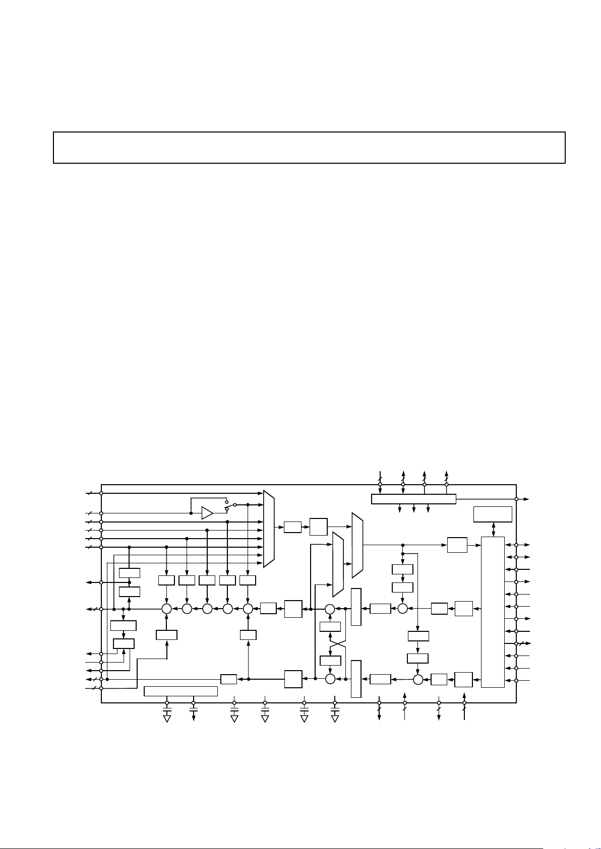
SIMPLIFIED FUNCTIONAL BLOCK DIAGRAM
20 dB
4
3
GNDA
V
CC
∑∆
ADC
GAM = GAIN
ATTENUATION
MUTE
GAM
GAM
FIFO
ADC
DAC1
DAC2
D
I
G
I
T
A
L
I
N
T
E
R
F
A
C
E
2
CONTROL
REGISTERS
LEFT AND
RIGHT CHANNELS
LEFT AND
RIGHT CHANNELS
GNDD
V
DD
FILTLCMOUT
V
REF
FILTR
4
2
HPOUTR
HPOUTC
HPOUTL
LOUT1
2
MOUT
2
2
2
MIN
AUX3
AUX2
AUX1
MIC
LIN
3
SYNC XTAL CONV BIT
CLKOUT
4
89
LOUT2
AAFILTL AAFILTR
1
SUM
RESET
PWRDWN
2
PDMNFT
MUTE
GAM GAM GAM GAM
GAM
GAM
MUTE
MUTE
MUTE
ATTN
2
3
ATTN
MUTE
S
E
L
E
C
T
O
R
MUTE
SCLK
SDFS
SDI
SDO
BM
CS
TSO
TSI
XCTL [1:0]
µ/A
LAW
3
CLOCK GENERATION
ATTN
M
U
T
E
MUTE
DRIVER
µ/A
LAW
FIFO
µ/A
LAW
S
E
L
E
C
T
O
R
S
E
L
E
C
T
O
R
PGA
∑∆
DAC
∑ ∑ ∑ ∑ ∑
∑∆
DAC
MUTE
∑
∑
∑
M
U
T
E
ATTN
∑
VOLTAGE REFERENCE
AD1843
Page 2

ANALOG INPUT
Min Typ Max Units
Full-Scale Input Voltage (RMS Values Assume Sine Wave Input)
All Inputs with ADRFLT & ADLFLT = 0 and LINLSD & LINRSD = 0 1 V rms
(LINLP, LINRP, AUX1L, AUX1R, AUX2L, 2.55 2.828 3.1 V p-p
AUX2R, AUX3L, AUX3R, MIN)
All Inputs with ADRFLT & ADLFLT = 0 and LINLSD & LINRSD = 1 2 V rms
(LINLP & LINLN, LINRP & LINRN) 5.1 5.656 6.2 V p-p
All Inputs with ADRFLT & ADLFLT = 1 and LINLSD & LINRSD = 0 1.127 V rms
(LINLP, LINRP, AUX1L, AUX1R, AUX2L, AUX2R, AUX3L, 2.8 3.156 3.5 V p-p
AUX3R, MIN)
All Inputs with ADRFLT & ADLFLT = 1 and LINLSD & LINRSD = 1 2.254 V rms
(LINLP & LINLN, LINRP & LINRN) 5.6 6.312 7.0 V p-p
MIC with +20 dB Gain (LMGE & RMGE = 1
and ADRFLT & ADLFLT = 0) 0.1 V rms
(MICL, MICR) 0.25 0.2828 0.31 V p-p
MIC with 0 dB Gain (LMGE & RMGE = 0
and ADRFLT & ADLFLT = 0) 1 V rms
(MICL, MICR) 2.55 2.828 3.1 V p-p
AUX, SUM and MIN Input Impedance* 10K Ω
(AUX1L, AUX1R, AUX2L, AUX2R, AUX3L, AUX3R, SUML,
SUMR, MIN)
LIN Input Impedance* (LINLP, LINLN, LINRP, LINRN) 40K Ω
MIC Input Impedance* (MICL, MICR) 20K Ω
Input Capacitance* (All Inputs) 15 pF
PROGRAMMABLE GAIN AMPLIFIER–ADC
Min Typ Max Units
Step Size (0 dB to 22.5 dB) (All Steps Tested) 1.3 1.5 1.7 dB
PGA Gain Range Span* 21.5 22.5 23.5 dB
INPUT (AUX1, AUX2, AUX3, MIN, MIC)
ANALOG AMPLIFIERS/ATTENUATORS
Min Typ Max Units
Step Size (+12.0 dB to –30 dB) (All Steps Tested) 1.25 1.5 1.75 dB
Step Size (–31.5 dB to –34.5 dB) (All Steps Tested) 1.1 1.5 1.9 dB
Input Gain/Attenuation Range* 45.5 46.5 47.5 dB
Mute Attenuation* –80.0 dB
AD1843–SPECIFICATIONS
REV. 0–2–
STANDARD TEST CONDITIONS UNLESS OTHERWISE NOTED
Temperature 25 °C
Digital Supply (V
DD
) 5.0 V
Analog Supply (V
CC
) 5.0 V
Sample Rate (F
S
) 48 kHz
Input Signal 1008 Hz
Analog Output Passband 20 Hz to 20 kHz
ADC FFT Size 2048
DAC FFT Size 8192
V
IH
2.0 V
V
IL
0.8 V
V
OH
2.4 V
V
OL
0.4 V
I
OH
–2 mA
I
OL
2mA
ADC Input Conditions
Mic 20 dB Gain Disabled
LIN Single-Ended
(LINLSD & LINRSD = 0)
Autocalibrated
0 dB PGA Gain
–1.0 dB Relative to Full Scale
Line Input
16-Bit Linear Mode
DAC Conditions
Autocalibrated
0 dB Attenuation
0 dB Relative to Full Scale
16-Bit Linear Mode
No Output Load
Mute Off
DAC1 Single-Ended
DAC2 Differential
Page 3

AD1843
REV. 0 –3–
DIGITAL DECIMATION AND INTERPOLATION FILTERS–AUDIO MODE*
Min Max Units
Passband 0 0.40 × F
S
Hz
Passband Ripple 0 –0.016 dB
Transition Band 0.4 × F
S
0.6 × F
S
Hz
Stopband
1
0.6 × F
S
Hz
Stopband Rejection 91.8 dB
Group Delay 15/F
S
s
Group Delay Variation Over Passband 0.0 µs
DIGITAL DECIMATION AND INTERPOLATION FILTERS–MODEM MODE*
Min Max Units
Passband 0 0.442 × F
S
Hz
Passband Ripple 0 –0.220 dB
Transition Band 0.442 × F
S
0.542 × FSHz
Stopband
2
0.542 × F
S
Hz
Stopband Rejection 75.7 dB
Group Delay 19/F
S
s
Group Delay Variation Over Passband 0.0 µs
Sample Rate 24 kHz
DIGITAL DECIMATION AND INTERPOLATION FILTERS–RESAMPLER MODE*
Min Max Units
Passband 0 0.4 × F
S
Hz
Passband Ripple 0 –0.035 dB
Transition Band 0.4 × F
S
0.5 × F
S
Hz
Stopband
3
0.5 × F
S
Hz
Stopband Rejection 92.2 dB
Group Delay 25/F
S
s
Group Delay Variation Over Passband 0.0 µs
ANALOG-TO-DIGITAL CONVERTERS
Min Typ Max Units
Audio Dynamic Range (–60 dB Input, THD+N Referenced to Full Scale,
A-Weighted, ADRFLT & ADLFLT = 0) 80 85 dB
Modem Dynamic Range (–60 dB Input, THD+N Referenced to Full Scale,
300 Hz to 4 kHz Analog Output Passband, LINRSD & LINLSD = 1,
ADRFLT & ADLFLT = 1, F
S
= 12.8 kHz) 87 90 dB
Audio THD+N (Referenced to Full Scale) 0.03 %
–74 –70 dB
Modem THD+N (–3.0 dB Referenced to Full Scale,
300 Hz to 4 kHz Analog Output Passband, LINRSD & LINLSD = 1,
ADRFLT & ADLFLT = 1, F
S
= 12.8 kHz) 0.02 %
–78.5 –74 dB
Audio Signal-to-Intermodulation Distortion* (CCIF Method) –94 –80 dB
ADC Crosstalk*
LIN Inputs (Input L, Ground R, Read R; Input R, Ground L, Read L) –80 dB
Line to MIC (Input LIN, Ground and Select MIC, Read Both Channels) –80 dB
Line to AUX1, AUX2, AUX3, MIN –80 dB
Interchannel Gain Mismatch (Difference of Gain Errors) ±0.5 dB
ADC Offset Error 10 50 mV
Page 4

REV. 0–4–
AD1843
DAC1 DIGITAL-TO-ANALOG CONVERTERS
Min Typ Max Units
Audio Dynamic Range (–60 dB Input, THD+N Referenced to Full Scale,
A-Weighted, DA1FLT = 0) 77 80 dB
Audio THD+N (Referenced to Full Scale, DA1FLT = 0) 0.03 %
–74 –70 dB
Audio Signal-to-Intermodulation Distortion* (CCIF Method) –92 –80 dB
Interchannel Gain Mismatch (Difference of Gain Errors) ±0.5 dB
DAC Crosstalk* (Input L, Zero R, Measure LOUT1R; Input R, Zero L,
Measure LOUT1L) –77 dB
Total Out-of-Band Energy*
(Measured from 0.6 × F
S
to 100 kHz in Audio Mode) –60 dB
Audible Out-of-Band Energy*
(Measured from 0.6 × F
S
to 22 kHz in Audio Mode,
Tested at FS = 8.0 kHz) –72 dB
DAC2 DIGITAL-TO-ANALOG CONVERTERS
Min Typ Max Units
Audio Dynamic Range (–60 dB Input, THD+N Referenced to Full Scale,
A-Weighted, DA2FLT = 0) 78 80 dB
Modem Dynamic Range (–60 dB Input, THD+N Referenced to Full Scale,
300 Hz to 4 kHz Analog Output Passband, DA2FLT = 1, RDA2G5:0
& LDA2G5:0 = 000101 [4.5 dB], F
S
= 12.8 kHz) 87 90 dB
Audio THD+N (Referenced to Full Scale, DA2FLT = 0) 0.03 %
–77 –70 dB
Modem THD+N (–3.0 dB Referenced to Full Scale,
300 Hz to 4 kHz Analog Output Passband, DA2FLT = 1, RDA2G5:0
& LDA2G5:0 = 000101 [4.5 dB], F
S
= 12.8 kHz) 0.016 %
–81 –76 dB
Audio Signal-to-Intermodulation Distortion* (CCIF Method) –86 –80 dB
Interchannel Gain Mismatch (Difference of Gain Errors) ±0.5 dB
DAC Crosstalk* (Input L, Zero R, Measure LOUT2R; Input R, Zero L,
Measure LOUT2L) –80 dB
Total Out-of-Band Energy*
(Measured from 0.6 × F
S
to 100 kHz in Audio Mode) –60 dB
Audible Out-of-Band Energy*
(Measured from 0.6 × F
S
to 22 kHz in Audio Mode,
Tested at F
S
= 8.0 kHz) –72 dB
DC Offset 525mV
DAC1 AND DAC2 ANALOG AMPLIFIERS/ATTENUATORS
Min Typ Max Units
Step Size (+12.0 dB to –30.0 dB) (All Steps Tested) 1.25 1.5 1.75 dB
Step Size (–31.5 dB to –34.5 dB) (All Steps Tested) 1.1 1.5 1.9 dB
Step Size (–36.0 dB to –82.5 dB)* 1.3 1.5 1.7 dB
Output Attenuation Span* 81.5 82.5 83.5 dB
Mute Attenuation* –80 dB
DIGITAL MIX ATTENUATORS
Min Typ Max Units
Step Size (0 dB to –94.5 dB)* (All Steps Tested) 1.3 1.5 1.7 dB
Output Attenuation Span* 93.5 94.5 95.5 dB
Mute Attenuation* –90 dB
Page 5
AD1843
REV. 0 –5–
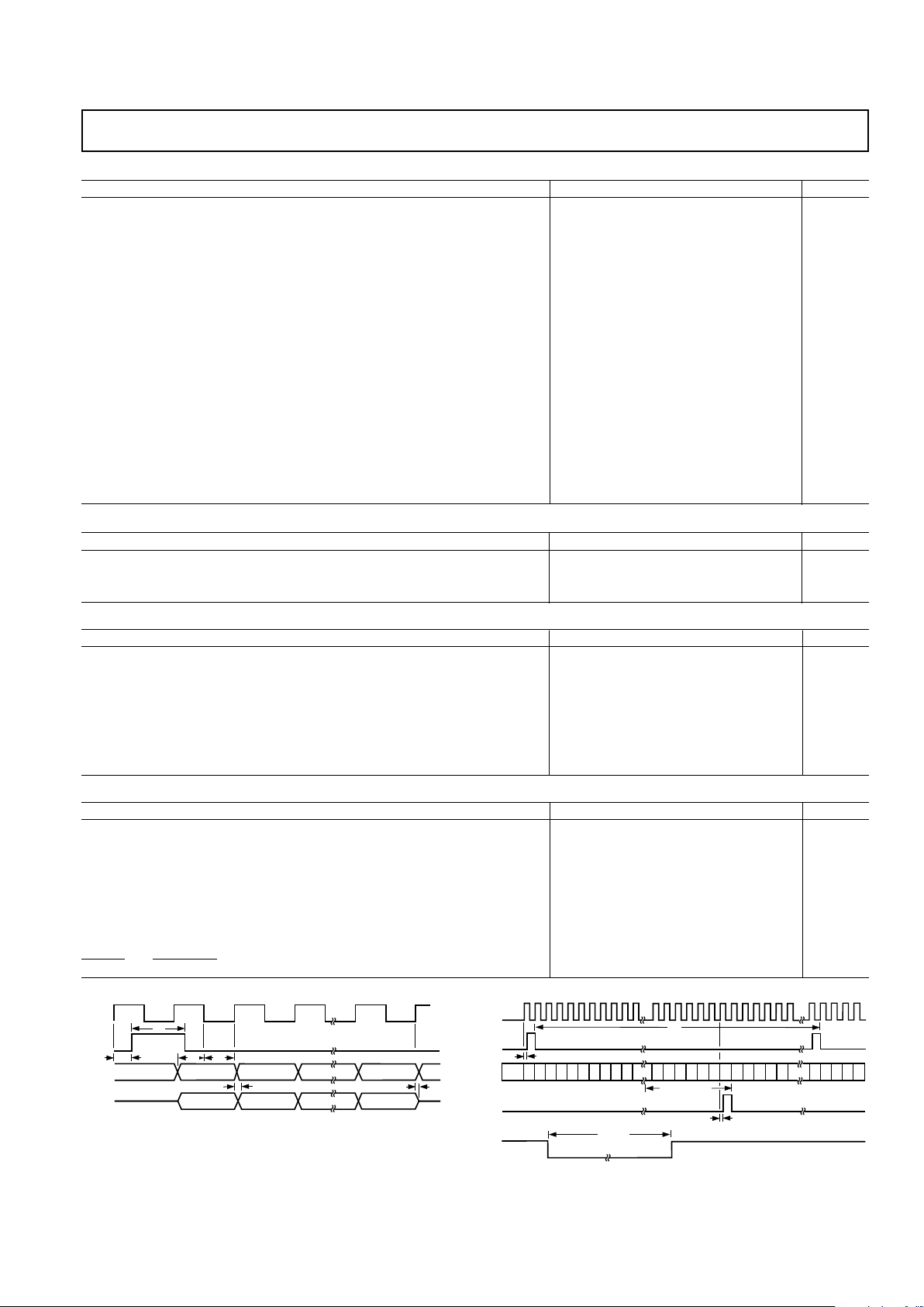
Figure 1. Timing Diagrams
ANALOG OUTPUT
Min Typ Max Units
LOUT1 Full-Scale Output Voltage 0.707 V rms
(RMS Values Assume Sine Wave Input) 1.8 2.0 2.2 V p-p
LOUT2 Full-Scale Single-Ended Output Voltage 0.707 V rms
(RMS Values Assume Sine Wave Input) 1.8 2.0 2.2 V p-p
LOUT2 Full-Scale Differential Output Voltage 1.414 V rms
(RMS Values Assume Sine Wave Input) 3.6 4.0 4.4 V p-p
LOUT1 Output Impedance* 600 Ω
LOUT2 Output Impedance* 1 Ω
LOUT1 External Load Impedance* 10 kΩ
LOUT2 External Load Impedance* 2 kΩ
MOUT External Load Impedance* 10 kΩ
HPOUT External Load Impedance* 16 32 Ω
HPOUT THD+N (Referenced to Full Scale, 32 Ω External Load Impedance) 0.10 %
–60 dB
Output Capacitance* 15 pF
External Load Capacitance* 100 pF
CMOUT 2.10 2.25 2.40 V
External CMOUT Load Current* 10 µA
CMOUT Output Impedance* 4 kΩ
Mute Click* (Muted Output Minus Unmuted Midscale DAC1 and DAC2 Outputs) ±5mV
SYSTEM SPECIFICATIONS
Max Units
System Frequency Response Ripple* (Line-In to Line-Out) 1.0 dB
Differential Nonlinearity* ±1 Bit
Phase Linearity Deviation* 5 Degrees
STATIC DIGITAL SPECIFICATIONS
Min Max Units
High-Level Input Voltage (V
IH
)
Digital Inputs, Except SCLK 2.0 V
DD
+ 0.3 V
XTALI and SCLK 2.4 V
DD
+ 0.3 V
Low-Level Input Voltage (V
IL
) –0.3 0.8 V
High-Level Output Voltage (V
OH
) 2.4 V
Low-Level Output Voltage (V
OL
) 0.4 V
Input Leakage Current (GO/NOGO Tested) –10 10 µA
Output Leakage Current (GO/NOGO Tested) –10 10 µA
TIMING PARAMETERS (GUARANTEED OVER OPERATING TEMPERATURE AND DIGITAL SUPPLY RANGE)
Min Typ Max Units
Serial Data Frame Sync [SDFS] Period (t
1
)
(Master Mode, FRS = 1 [16 Slots per Frame], SCF = 0 [SCLK = 12.288 MHz]) 20.833 µs
Frame Sync [SDFS] HI Pulse Width (t
2
)80ns
Clock [SCLK] to Frame Sync [SDFS] Propagation Delay (t
PD1
)15ns
Data [SDI] Input Setup Time to SCLK (t
S
)10ns
Data [SDI] Input Hold Time from SCLK (t
H
)10 ns
Clock [SCLK] to Output Data [SDO] Valid (t
DV
)15ns
Clock [SCLK] to Output Data [SDO] Three-State [High-Z] (t
HZ
)15ns
Clock [SCLK] to Time Slot Output [TSO] Propagation Delay (t
PD2
)15ns
RESET and PWRDWN LO Pulse Width (t
RPWL
) 100 ns
t
2
BIT 0BIT 14BIT 15
BIT 15 BIT 14 BIT 0
t
PD1
SCLK
SDFS
SDI
SDO
tSt
H
t
DV
t
HZ
RESET
PWRDWN
t
RPWL
1514 13
3 2 1 0 15 14 13
t
PD2
t
PD1
SCLK
SDFS
SDI OR SDO
TSO
LAST
VALID
TIME SLOT
t
1
151413
Page 6
REV. 0–6–
AD1843
POWER SUPPLY (33 Ω HPOUT LOAD)
Min Typ Max Units
Power Supply Range—Analog V
CC
4.75 5.25 V
Power Supply Range—Digital V
DD
2.85 5.25 V
Total Power Supply Current—5.0 V
CC
and VDD Operating
(5.0 V
CC
and V
DD
Supplies) 210 250 mA
Total Power Supply Current—5.0 V
CC
/3.0 VDD Operating*
(5.0 V
CC
Analog/3.0 VDD Digital Supplies) 150 175 mA
Analog Supply Current—5.0 V
CC
Operating 60 75 mA
Digital Supply Current—5.0 V
DD
Operating 150 175 mA
Digital Supply Current—3.0 V
DD
Operating* 90 100 mA
Digital Power Supply Current—V
DD
Power Down (PWRDWN LO) 1 mA
Analog Power Supply Current—V
CC
Power Down (PWRDWN LO) 0.5 mA
Power Dissipation—5.0 V
CC
and VDD Operating (Current × Nominal Supply) 1250 mW
Power Dissipation—5.0 V
CC
/3.0 VDD Operating* (Current × Nominal Supply) 875 mW
Power Dissipation—5.0 V
CC
and VDD Power Down (PWRDWN LO)
(Current × Nominal Supply) 7.5 mW
Power Dissipation—5.0 V
CC
/3.0 VDD Power Down* (PWRDWN LO)
(Current × Nominal Supply) 5mW
Power Supply Rejection (100 mV p-p Signal @ 1 kHz)* 40 dB
(At Both Analog and Digital Supply Pins, for ADC, DAC1 and DAC2)
CLOCK SPECIFICATIONS*
Min Typ Max Units
Input Crystal/Clock Frequency 24.576 MHz
Input Clock Duty Cycle (When an External Clock Is Used Instead of a Crystal) 25/75 75/25 %
Initialization Sample Rate Change Time 0 ms
PACKAGE CHARACTERISTICS
Typ Units
PQFP θ
JA
(Thermal Resistance [Junction-to-Ambient]) 96 °C/W
PQFP θ
JC
(Thermal Resistance [Junction-to-Case]) 8.75 °C/W
TQFP θ
JA
(Thermal Resistance [Junction-to-Ambient]) 30.6 °C/W
TQFP θJC (Thermal Resistance [Junction-to-Case]) 4.6 °C/W
NOTES
1
The stopband repeats itself at multiples of 64 × FS, where FS is the sampling frequency. Thus the audio mode digital filter will attenuate to –91.8 dB or better across
the frequency spectrum except for a range of ±0.6 × F
S
wide at multiples of 64 × FS.
2
The stopband repeats itself at multiples of 64 × FS, where FS is the sampling frequency. Thus the modem mode digital filter will attenuate to –75.7 dB or better across
the frequency spectrum except for a range of ±0.542 × F
S
wide at multiples of 64 × FS.
3
The stopband repeats itself at multiples of 64 × FS, where FS is the sampling frequency. Thus the resampler mode digital filter will attenuate to –92.2 dB or better
across the frequency spectrum except for a range of ±0.5 × F
S
wide at multiples of 64 × FS.
*Guaranteed, not tested.
Specifications subject to change without notice.
ABSOLUTE MAXIMUM RATINGS*
Min Max Units
Power Supplies
Digital (V
DD
) –0.3 6.0 V
Analog (V
CC
) –0.3 6.0 V
Input Current
(Except Supply Pins) ±10.0 mA
Analog Input Voltage (Signal Pins) –0.3 V
CC
+ 0.3 V
Digital Input Voltage (Signal Pins) –0.3 V
DD
+ 0.3 V
Ambient Temperature (Operating) 0 +70 °C
Storage Temperature –65 +150 °C
ESD Tolerance (Human Body 1000 V
Model per Method 3015.2
of MIL-STD-883B)
WARNING!
ESD SENSITIVE DEVICE
CAUTION
ESD (electrostatic discharge) sensitive device. Electrostatic charges as high as 4000 V readily
accumulate on the human body and test equipment and can discharge without detection.
Although the AD1843 features proprietary ESD protection circuitry, permanent damage may
occur on devices subjected to high energy electrostatic discharges. Therefore, proper ESD
precautions are recommended to avoid performance degradation or loss of functionality.
*Stresses greater than those listed under “Absolute Maximum Ratings” may cause
permanent damage to the device. This is a stress rating only and functional
operation of the device at these or any other conditions above those indicated in the
operational section of this specification is not implied. Exposure to absolute
maximum rating conditions for extended periods may affect device reliability.
ORDERING INFORMATION
Temperature Package Package
Model Range Description Option
AD1843JS 0°C to +70°C 80-Lead PQFP S-80
AD1843JST 0°C to +70°C 100-Lead TQFP ST-100
Page 7
AD1843
REV. 0 –7–
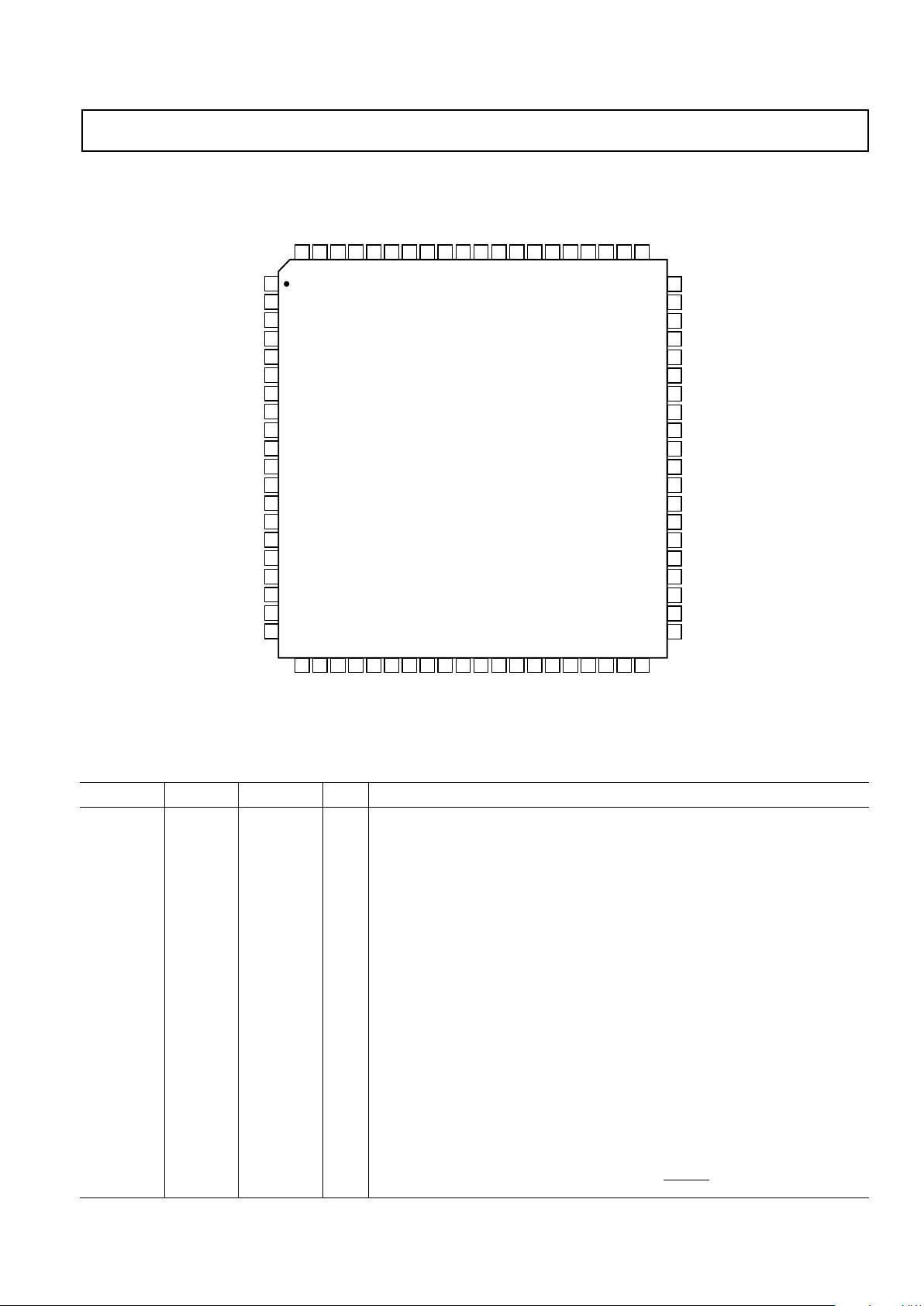
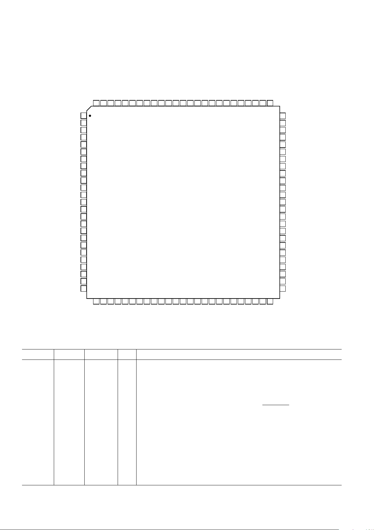
PIN CONFIGURATIONS
80-Lead PQFP
79 78 77 76 75 74 73 72 71 70 69 68 67 66 65 64 63 6280 61
1
2
3
4
5
6
7
8
9
10
11
12
13
14
15
16
17
18
19
20
21 22 23 24 25 26 27 28 29 30 31 32 33 34 35 36 37 38 39 40
41
42
43
44
45
46
47
48
49
50
51
52
53
54
55
56
57
58
59
60
AD1843
TOP VIEW
(Not to Scale)
SDI
SCLK
GNDD
V
DD
CLKOUT
CONV3
V
DD
V
DD
VDDV
DD
BIT3
GNDD
CONV2
CONV1
BIT2
GNDD
GNDD
BIT1
XTALO
XTALI
GNDD
XCTL1
XCTL0
SYNC3
SYNC2
SYNC1
GNDD
V
DD
RESET
PWRDWN
V
DD
PDMNFT
GNDA
HPOUTL
HPOUTC
HPOUTR
V
CC
SUML
SUMR
V
CC
V
DD
V
CC
SDO
SDFS
GNDD
TSI
TSO
GNDD
V
DD
CS
BM
AUX3R
AUX3L
AUX2R
AUX2L
AUX1R
AUX1L
MICR
MICL
MIN
GNDA
AAFILTR
FILTR
AAFILTL
FILTL
LINRP
LINRN
LINLP
LINLN
LOUT2RP
LOUT2RN
LOUT2LP
LOUT2LN
MOUT
LOUT1L
GNDA
CMOUT
V
REF
GNDA
LOUT1R
PIN DESCRIPTION
Serial Interface
Pin Name PQFP TQFP I/O Description
SCLK 79 99 I/O Serial Clock. SCLK is a bidirectional signal that supplies the clock as an output
to the serial bus when the Bus Master (BM) pin is driven HI and accepts the clock
as an input when the BM pin is driven LO. When the AD1843 is configured in
master mode, the SCLK frequency may be set to either 12.288 MHz or 16.384 MHz
with the SCF bit in Control Register Address 26.
SDFS 2 2 I/O Serial Data Frame Sync. SDFS is a bidirectional signal that supplies the frame
synchronization signal as an output to the serial bus when the Bus Master (BM)
pin is driven HI and accepts the frame synchronization signal as an input when
the BM pin is driven LO.
SDI 80 100 I Serial Data Input. SDI is used by peripheral devices such as the host CPU or a
DSP to supply control and playback data information to the AD1843. All control
and playback transfers are 16 bits long, MSB first.
SDO 1 1 O Serial Data Output. SDO is used to supply status/control register readback and
capture data information to peripheral devices such as the host CPU or a DSP.
All status/control register readback and capture data transfers are 16 bits long,
MSB first. A three-state output driver is used on this pin.
BM 10 12 I Bus Master. When BM is tied HI the AD1843 is the serial bus master. The
AD1843 will then supply the serial clock (SCLK) and the frame sync (SDFS)
signals for the serial bus. No more than one device (AD1843/CPU/DSP) should
be configured as the serial bus master. When BM is tied LO, the AD1843 is configured as a bus slave, and will accept the SCLK and SDFS signals as inputs. The
logic level on this pin must not be changed once RESET is deasserted (driven HI).
Page 8
REV. 0–8–
AD1843
26 272829 30 313233 34 35 36 37 38 39 40 41 42 43 44 45 46 47 48 49 50
51
52
53
54
55
56
57
58
59
60
61
62
63
64
65
66
67
68
69
70
71
72
73
74
75
1
2
3
4
5
6
7
8
9
10
11
12
13
14
15
16
17
18
19
20
21
22
23
24
25
99 98 97 96 95 94 93 92 91 90 89 88 87 86 85 84 83 82 81 80 79 78 77100 76
AD1843
TOP VIEW
(Not to Scale)
SDI
SCLK
NC
GNDD
V
DD
CLKOUT
CONV3
NC
NC
NC
NC
V
DD
V
DD
VDDV
DD
BIT3
GNDD
CONV2
CONV1
BIT2
GNDD
GNDD
BIT1
XTALO
XTALI
GNDD
XCTL1
NC
XCTL0
SYNC3
SYNC2
SYNC1
NC
GNDD
V
DD
RESET
PWRDWN
NC
V
DD
PDMNFT
NC
GNDA
HPOUTL
HPOUTC
HPOUTR
V
CC
SUML
SUMR
NC
V
CC
NC
NC
NC
NC
NC
GNDA
AAFILTR
FILTR
AAFILTL
FILTL
LINRP
LINRN
LINLP
LINLN
LOUT2RP
LOUT2RN
LOUT2LP
LOUT2LN
LOUT1R
MOUT
LOUT1L
GNDA
CMOUT
V
REF
GNDA
NC
V
DD
V
CC
NC
NC
NC
NC
SDO
SDFS
GNDD
TSI
TSO
GNDD
V
DD
CS
BM
AUX3R
AUX3L
AUX2R
AUX2L
AUX1R
AUX1L
MICL
MICR
MIN
NC = NO CONNECT
Serial Interface (Continued)
Pin Name PQFP TQFP I/O Description
CS 9 11 I Chip Select. When CS is set HI, the serial interface I/O pins will be in their normal
active states. When CS is reset LO, SCLK, SDFS, and SDO are threestated; SCLK, SDFS and SDI inputs are ignored; and TSO drives out the logic
level received on TSI.
TSO 6 7 O Time Slot Output. TSO is asserted HI by the AD1843 simultaneously with the LSB
of the last time slot used by the AD1843. It is used to daisy-chain multiple AD1843s
on a common TDM serial bus. If the power-down (
PWRDWN) pin is asserted or if
the chip select pin (CS) is deasserted, TSO is set to the logic level on the TSI pin,
allowing powered-down or unselected AD1843s on a daisy-chain to be skipped.
TSI 5 6 I Time Slot Input. Asserting TSI HI indicates to the AD1843 that it should use
the next six time slots beginning on the next SCLK period. It also enables TSO
to be asserted at the end of these six time slots. TSI is ignored (but should be tied
LO) when the AD1843 is the bus master since the bus master uses the first time
slots in a TDM frame.
XCTL[1:0] 59, 58 72, 74 I/O External Control. These signals reflect the status of bits (Data 8 and 9) in Control
Register Address 28 of the AD1843. They may be used for signaling or controlling
external logic.
PIN CONFIGURATIONS
100-Lead TQFP
Page 9

AD1843
REV. 0 –9–
Analog Signals
Pin Name PQFP TQFP I/O Description
LINLP 28 35 I Line Input Left Channel Positive Differential Signal.
LINLN 29 36 I Line Input Left Channel Negative Differential Signal.
LINRP 26 33 I Line Input Right Channel Positive Differential Signal.
LINRN 27 34 I Line Input Right Channel Negative Differential Signal.
MICL 18 21 I Microphone Input Left Channel. Microphone input for the left channel. This
signal can be either line level or –20 dB from line level.
MICR 17 22 I Microphone Input Right Channel. Microphone input for the right channel.
This signal can be either line level or –20 dB from line level.
AUX1L 16 20 I Auxiliary #1 Left Channel Line Input.
AUX1R 15 19 I Auxiliary #1 Right Channel Line Input.
AUX2L 14 18 I Auxiliary #2 Left Channel Line Input.
AUX2R 13 17 I Auxiliary #2 Right Channel Line Input.
AUX3L 12 16 I Auxiliary #3 Left Channel Line Input.
AUX3R 11 15 I Auxiliary #3 Right Channel Line Input.
MIN 19 23 I Monaural (Mono) Line Input.
MOUT 35 44 O Monaural (Mono) Line Output.
LOUT1L 36 45 O Line Output #1 Left Channel.
LOUT1R 34 43 O Line Output #1 Right Channel.
HPOUTL 47 58 O Headphone Output Left Channel.
HPOUTC 46 57 Headphone Common Return.
HPOUTR 45 56 O Headphone Output Right Channel.
LOUT2LP 32 40 O Line Output #2 Left Channel Positive Differential Signal.
LOUT2LN 33 41 O Line Output #2 Left Channel Negative Differential Signal.
LOUT2RP 30 38 O Line Output #2 Right Channel Positive Differential Signal.
LOUT2RN 31 39 O Line Output #2 Right Channel Negative Differential Signal.
SUML 43 54 I Mixer Line Input Left Channel.
SUMR 42 53 I Mixer Line Input Right Channel.
Clocks
Pin Name PQFP TQFP I/O Description
CLKOUT 76 95 O Clock Output. This signal is a buffered version of XTALO (with a duty cycle
restored to at least 60%/40%), the crystal clock output. This pin is enabled by
default but can be three-stated by programming a bit in Control Register
Address 28. The CLKOUT frequency is 24.576 MHz.
SYNC[3:1] 57, 56, 55 71, 70, 69 I Sync Inputs. These SYNC signals are used as the clock source inputs to three
receptive PLLs in the AD1843. These pins accept a clock at, or at a multiple of,
the desired sample rate for A-to-D and D-to-A conversions. These inputs are
ignored if a sample rate is programmed directly, but should never be left floating.
CONV[3:1] 75, 71, 67 94, 89, 84 O Conversion Clock Outputs. These output clocks have an average period equal to (or 128
times) the internal sample rates of the AD1843. These clock outputs are three-stated
by default but can be enabled by programming bits in Control Register Address 28.
BIT[3:1] 74, 70, 66 92, 87, 82 O Bit Clock Outputs. These output clocks can be individually programmed to
multiples of the sample rates. Support for V.34 or V.32 bit rates is available.
These clock outputs are three-stated by default but can be enabled by
programming bits in Control Register Address 28.
Page 10
REV. 0–10–
AD1843
Miscellaneous
Pin Name PQFP TQFP I/O Description
XTALI 61 76 I 24.576 MHz Crystal Input. When using a crystal as the clock source, the crystal
should be connected between the XTALI and XTALO pins. This crystal should
be 24.576 MHz for the normal sampling rate range, i.e., 4 kHz to 54 kHz. A
clock input (perhaps the CLKOUT of another AD1843) may be driven into
XTALI in place of a crystal. The external clock input must be greater than or equal
to 512 times the maximum desired AD1843 sampling frequency.
XTALO 62 77 O 24.576 MHz Crystal Output. When using a crystal as the clock source, the crystal
should be connected between the XTALI and XTALO pins. If a clock is driven
directly into XTALI, then XTALO should be left unconnected.
PWRDWN 51 64 I Power Down. PWRDWN is active LO. The assertion of this signal will initialize
the on-chip Control Registers to their default values, and will completely and
quietly power down the AD1843. If a crystal is not connected between XTALI
and XTALO, there must be a 24.576 MHz clock input on XTALI for at least
5 ms after this signal is asserted LO for proper operation. The AD1843 will not
be completely powered down until after this 5 ms period elapses. The AD1843
always finishes an in-progress power-up sequence before initiating a power-down
sequence, and vice versa. If the
PWRDWN pin is asserted while a power-up sequence
is in progress, the 24.576 MHz clock signal on XTALI must persist for a worst
case maximum of 479 ms (power up = 470 ms, autocalibration = 4 ms, power
down = 5 ms) after
PWRDWN is asserted. When INIT (Control Register
Address 0, Bit 15) is set to a “1,” the power-down sequence is complete. See
the “Power Management” section for important additional details.
RESET 52 65 I Reset. RESET is active LO. The assertion of this signal will initialize the on-chip
registers to their default values, and will completely power down the AD1843.
RESET is similar to PWRDWN, except that when PWRDWN is asserted, power
down is “quiet” and performed synchronously to the internal clocks. When
RESET
is asserted, power down is “noisy” and performed asynchronously to the internal
clocks.
PDMNFT 49 61 I Power-Down Mono Feedthrough. When the AD1843 mixer is powered down,
and PDMNFT is asserted HI, the Mono Input (MIN, PQFP Pin 19) is routed to
the Mono Output (MOUT, PQFP Pin 35), and the signal applied to MIN will
feedthrough to MOUT. When the AD1843 mixer is powered down and
PDMNFT is deasserted LO, the feedthrough of MIN to MOUT will be muted.
When the AD1843 mixer is not powered down, and MIN to MOUT feedthrough
is desired, the Mono Input Mix Mute (Control Register Address 8, Bit 15) and the
Mono Output Mute (Control Register Address 8, Bit 6) must be unmuted. During
power-down feedthrough, the signal applied to the MIN input appears only at
the MOUT output. During normal operation, the signal applied to the MIN
input appears at both the MOUT and the LOUT1 outputs. The state of the
PDMNFT pin should be changed when the AD1843 mixer is powered up. If the
state of PDMNFT is changed when the AD1843 is in total power-down, audible
pops and clicks will likely result.
CMOUT 38 47 O Common-Mode Voltage Output. Nominal 2.25 volt reference available externally
for dc-coupling and level-shifting. CMOUT should not be used where it will sink
or source current.
V
REF
39 48 I Voltage Reference Filter. Voltage reference filter point for external bypassing only.
FILTL 25 31 I Left Channel Filter. This pin requires a 1.0 µF capacitor to analog ground for
proper operation.
FILTR 23 29 I Right Channel Filter. This pin requires a 1.0 µF capacitor to analog ground for
proper operation.
AAFILTL 24 30 I Left Channel Antialias Filter. This pin requires a 1000 pF capacitor to analog
ground for proper operation.
AAFILTR 22 28 I Right Channel Antialias Filter. This pin requires a 1000 pF capacitor to analog
ground for proper operation.
Page 11

AD1843
REV. 0 –11–
POWER SUPPLIES
Pin Name PQFP TQFP I/O Description
V
CC
20, 41, 44 25, 51, 55 I Analog Supply Voltage (+5 V).
GNDA 21, 37, 40, 48 27, 46, 49, 59 O Analog Ground.
V
DD
4, 8, 50, 53, 5, 10, 62, 66, I Digital Supply Voltage (+5/3 V).
63, 64, 68, 72, 79, 80, 85, 90,
77 96
GNDD 3, 7, 54, 60, 4, 9, 67, 75, I Digital Ground.
65, 69, 73, 78 81, 86, 91, 97
NC 3, 8, 13, 14, No Connect. May be left floating.
24, 26, 32, 37,
42, 50, 52, 60,
63, 68, 73, 78,
83, 88, 93, 98
(continued from page 1)
The versatility of the device is shown by the following examples
of functions it can perform:
• Stereo audio input and/or quad output, simultaneously at dif-
ferent sample rates
• Stereo audio output with simultaneous full duplex modem or
fax operation with frequency and phase resampling
• Mono audio input and stereo audio output with simultaneous
modem receive and transmit for simultaneous voice and data
communications
• Dual independent audio inputs with audio output for echo-
cancelling speakerphones
Audio Functional Description
The AD1843 SoundComm codec provides a complete audio solution with very few external components required. Dynamic
range of the device exceeds 80 dB over the 20 kHz audio band
and sample rates from 4 kHz to 49 kHz are supported (up to
54 kHz for a single channel if other channels are powered
down). The audio functionality of this device is a superset of
that found in the Analog Devices AD1848 SoundPort
®
device
which has set the business audio standard throughout the computer industry.
Inputs to the device include a stereo microphone pair, a stereo
line pair, a stereo CD input pair (AUX1), a stereo synthesized
music input pair (AUX2), a dual phone line input (AUX3), a
mono input, and a stereo input from an FM synthesizer (SUM).
All of these inputs (except SUM) are multiplexed to the two ∑∆
A/D converters and are mixable directly as analog signals with
the outputs of the D/A converters. All analog input signals (except SUM) can be amplified, attenuated or muted before mixing with the outputs of the D/A converters.
The device has two pairs of ∑∆ DACs which accept 8- or 16-bit
digital data from the serial port. Each DAC pair’s independent
sampling rate can either be programmed by Control Register
(with 1 Hz resolution) or synchronized to an external input.
The second pair of DACs can be used to replace the music synthesis DAC pair found on many audio products for PCs. Outputs from the AD1843 include a line output, a mono output, a
stereo headphone output with its own current return path, and a
SoundPort is a registered trademark of Analog Devices, Inc.
differential stereo output for connection to a DAA. The line and
differential outputs are looped back to the ADC input selector.
The AD1843’s mixing and routing capabilities are extensive.
The digital data from both DAC channels after interpolation
can be routed back to the ADC decimators, to support digitalto-digital sample rate conversion (digital resampling). Digital
data from the ADC can also be routed to the two stereo DAC
pairs, for a digital loopback mode which is helpful for devicelevel and board-level test. Digital data from either stereo DAC
can be mixed with the digital data feeding the other DAC, and
the analog signal from DAC2 can be mixed with the analog output from DAC1.
Sample rates are independently programmable in the range of
4 kHz to 54 kHz to a 1 Hz resolution or sample rates can be
synchronized to an external source. Up to three different signals
can be applied to the device’s three digital phase lock loop
SYNC inputs for external synchronization.
These SYNC inputs can also be used in a special mode for audio/video synchronization. In this mode, an NTSC or PAL derived clock signal (approximately 15 kHz) is applied to the
SYNC inputs and the device produces one of a variety of standard audio sample rates (32 kHz, 44.056 kHz, 44.1 kHz and
48 kHz, and most of these divided by the integers 1 through 8).
In this manner, video and audio sample rates which are mathematically unrelated can be locked together.
Data Communications/Telephony Functional Description
The AD1843 includes all data conversion, filtering, and clock
generation circuitry needed to implement an echo-cancelling
modem with a companion digital signal processor. Softwareprogrammable sample rates and clocking modes support all
established modem standards including those for the V.34
standard.
The AD1843 utilizes advanced ∑∆ technology to move the
entire echo-cancelling modem implementation into the digital
domain. The device maintains 90 dB typical dynamic range
throughout all filtering and data conversion across a 9.6 kHz
passband. Purely DSP-based echo cancellation algorithms can
maintain robust bit error rates under worst-case signal attenuation and echo amplitude conditions. The AD1843’s on-chip
interpolation filter resamples (both frequency and phase) the received signal after echo cancellation in the DSP, freeing the processor for other voice or data communications tasks.
Page 12
REV. 0–12–
AD1843
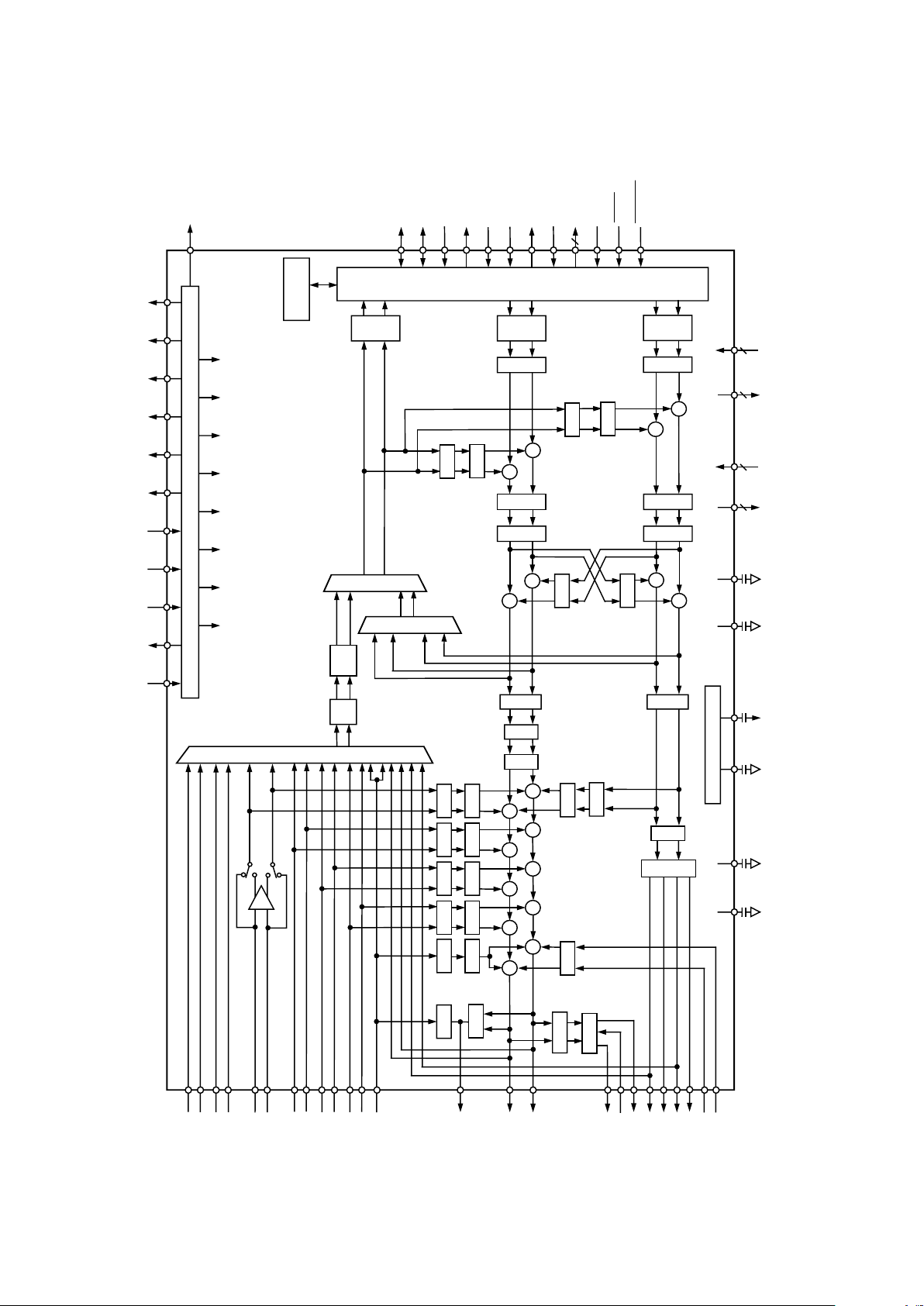
Figure 2. Detailed Functional Block Diagram
8 9
GNDD
V
DD
FILTL
CMOUT
V
REF
FILTR
∑
S
ELE
C
T
O
R
CLOCK GENERATION
HPOUTR
HPOUTC
HPOUTL
LOUT2LP
LOUT2LN
LOUT2RP
LOUT2RN
CLKOUT
2
LEFT
RIGHT
LEFT
RIGHT
GN/AT
MUTE
SELECTO
R
20 dB
LEFT
RIGHT
43
GNDA
V
CC
ADC
DAC1
DAC2
D
IGI
TAL
I
NTE
RFACE
LOUT1L
LOUT1R
AUX3L
AUX2R
AUX1L
AUX2L
AUX1R
LINRP
LINRN
MICR
MICL
GN/AT = GAIN/
ATTENUATION
DRIVER
CONTROL
REGISTERS
AD1843
AAFILTL
AAFILTR
SUML
SUMR
LINLP
LINLN
MOUT
RESET
PWRDWN
∑
GN/AT
MUTE
∑
GN/AT
MUTE
∑
∑
GN/AT
MUTE
∑
∑
GN/AT
MUTE
∑
GN/AT
MUTE
∑
∑
MUTE
MUTE
GN/AT
MUTE
MUTE
∑∆
DAC
∑
∑
MUTE
MUTE
ATTN
∑
∑
MUTE
MUTE
∑
∑
MUTE
ATTN
MUTE
MUTE
GN/AT
ATTN
∑
∑
MUTE
ATTN
FIFO
µ/A
LAW
AUX3R
MIN
FIFO
µ/A
LAW
S
ELE
C
T
O
R
∑∆
ADC
PGA
µ/A
LAW
XTALI XTALO SYNC3 SYNC2 SYNC1 CONV3 CONV2 CONV1 BIT3 BIT2 BIT1
SCLK
SDFS
SDI
SDOBMCS
TSO
TSI
XCTL [1:0]
PDMNFT
VOLTAGE REFERENCE
∑∆
DAC
Page 13
AD1843
REV. 0 –13–
On-chip bit and baud clock generation circuitry allows either
synchronous or asynchronous operation of the transmit (DAC)
and receive (ADC) paths. Each path features independent
phase advance and retard adjustments via software control. The
AD1843 can also synchronize modem operation to an external
terminal band clock. Because the device has multiple input and
output channels and converters, it is well suited for telephony
applications requiring multiple channels for voice and modem.
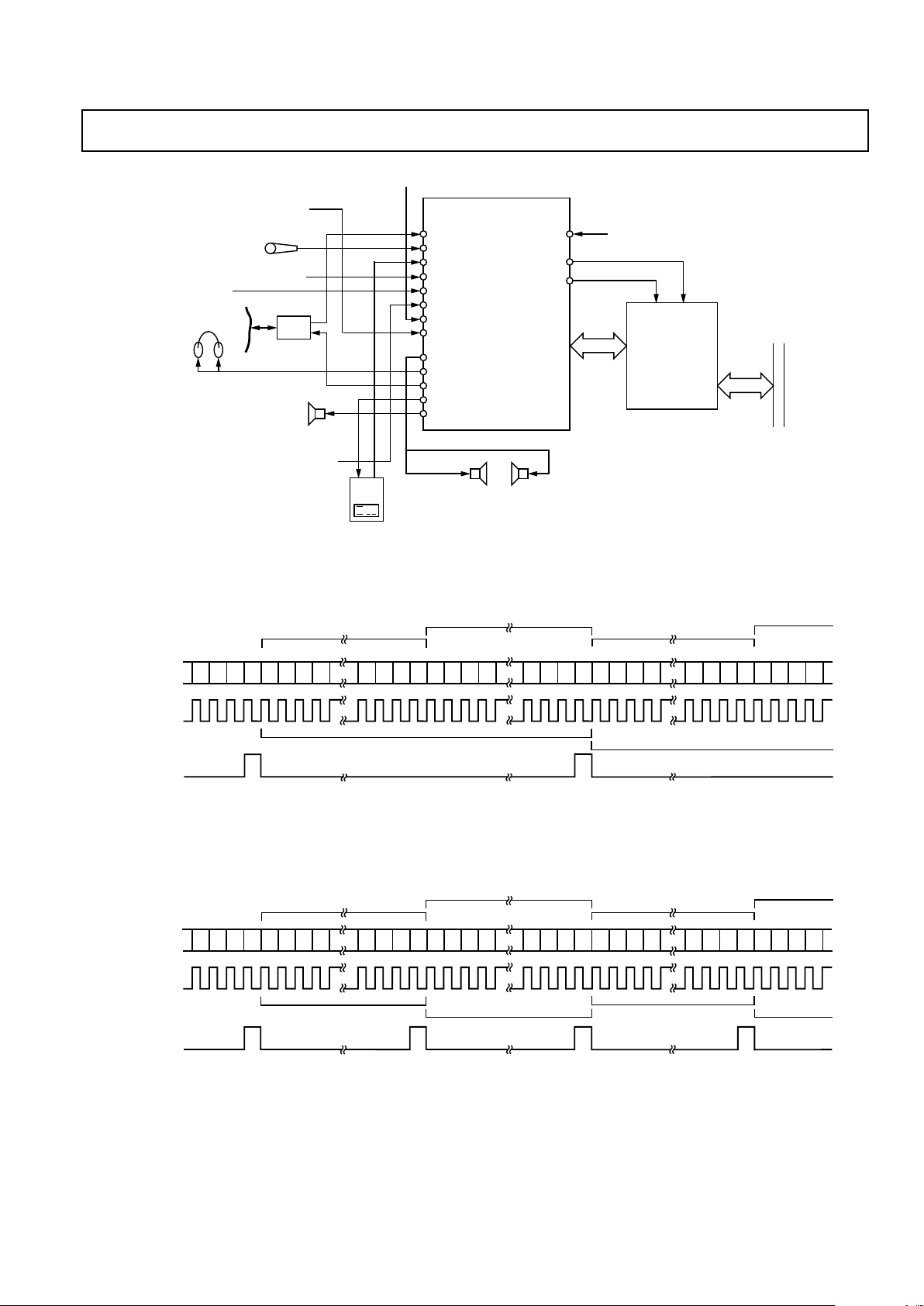
A detailed block diagram of the AD1843 is shown in Figure 2.
DETAILED PRODUCT DESCRIPTION
The Serial-Port AD1843 SoundComm Codec integrates the key
audio and PSTN data conversion and control functions into a
single integrated circuit. The AD1843 is intended to provide a
complete, single-chip audio and fax/modem solution for PC
multimedia applications.
External circuit requirements are limited to a minimal number
of low cost support components. Dynamic range exceeds 80 dB
over the 20 kHz audio band. Sample rates from 4 kHz to
54 kHz with 1 Hz resolution are supported from a single external crystal or clock source.
The AD1843 SoundComm Codec is intended to be interfaced
through a DSP chip or an ASIC to a host bus such as ISA,
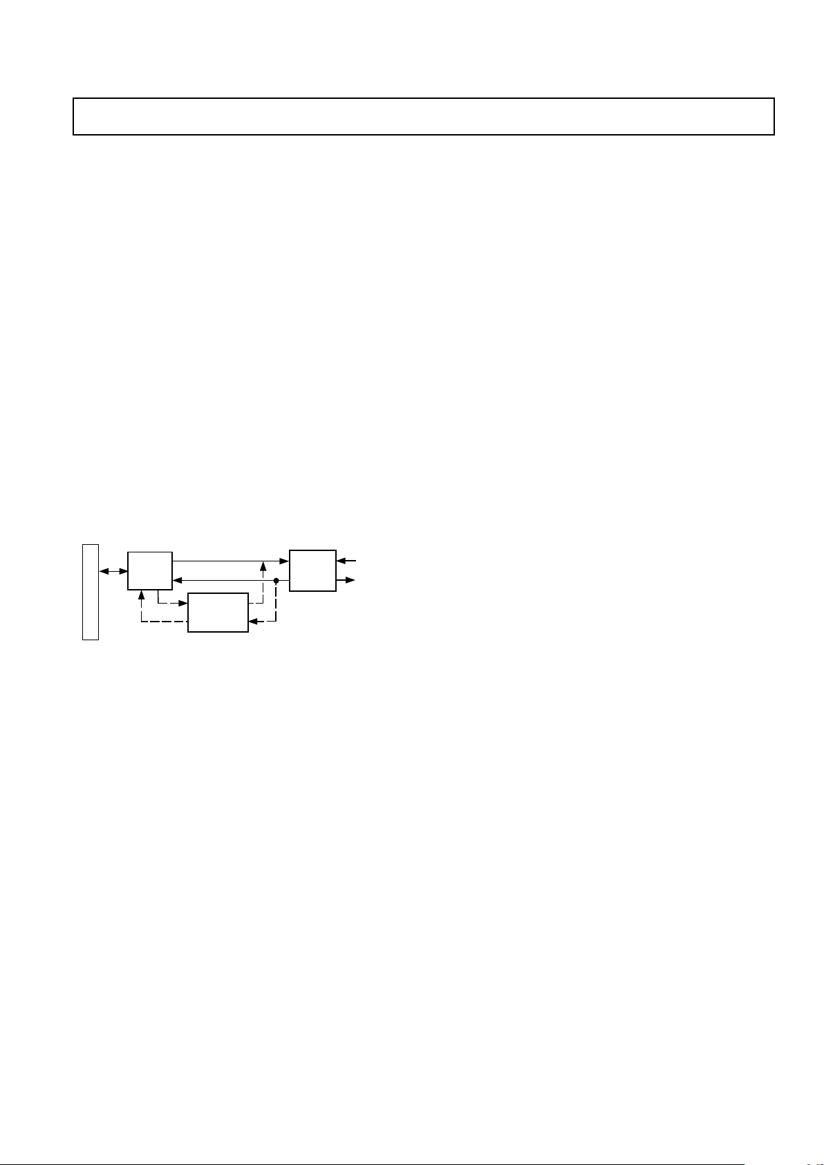
EISA or PCI. A general system architecture is shown in
Figure 3.
S
Y
S
T
E
M
B
U
S
ASIC
ADSP-21xx
ANALOG I/O
AD1843
Figure 3. AD1843 System Diagram
The SoundComm codec includes a stereo pair of ∑∆ analog-todigital converters and two stereo pairs of ∑∆ digital-to-analog
converters. Inputs to the ADC can be selected from eight
sources of analog signals: stereo line (LIN), stereo microphone
(MIC), stereo auxiliary line #1 (AUX1), stereo auxiliary line #2
(AUX2), stereo auxiliary line #3 (AUX3), mono line (MIN),
mixer output, and DAC2 output. A mono output and a stereo
headphone driver are included on-chip. A stereo line level input
(SUM) can be mixed into the output summer. A software-controlled programmable gain stage allows independent gain for
each ADC channel. The ADCs’ output can be digitally mixed
with both the DAC1 and DAC2 inputs. The left and right
ADC channels can be configured for different sample rates and
digital filter function (audio, modem or resampling).
The pair of 16-bit outputs from the ADCs is available over a serial interface that also supports 16-bit digital input to the DACs
and control/status information. The AD1843 can accept and
generate 16-bit twos-complement PCM linear digital data, 8-bit
unsigned magnitude PCM linear data, and 8-bit µ-law or A-law
companded digital data. The data format is defined independently for each conversion resource on the AD1843.
The ∑∆ DACs are preceded by a four sample deep FIFO buffer
and a digital interpolation filter. The DAC1 and DAC2 outputs
can be mixed in the digital domain. Digital and analog attenuators provide independent user volume control (plus mute) over
each DAC channel. Nyquist images and shaped quantized
noise are removed from the DACs’ analog stereo output by onchip switched-capacitor and continuous-time filters. All of the
analog inputs (except the stereo line input) can be mixed with
the DAC1 output in the analog domain. The DAC2 output can
also be mixed with the DAC1 output in the analog domain.
The DAC1 and DAC2 digital data can be fed back to the digital
half of the ADC to enable digital resampling operation. DAC1
and DAC2 can be run at different sample rates and with different digital filter functions, without any beat frequency problems.
FUNCTIONAL DESCRIPTION
This section overviews the functionality of the AD1843 and is
intended as a general introduction to the capabilities of the device. As much as possible, detailed reference information has
been placed in “Control Registers” and other sections. The
user is not expected to refer repeatedly to this section.
Analog Inputs
The AD1843 SoundComm Codec accepts stereo line-level and
mic-level inputs. The mono MIN analog signal input, and LIN
(differential), MIC, AUX1, AUX2, AUX3 and post-mixed
DAC output analog stereo signals are multiplexed to the internal programmable gain amplifier stage (PGA).
The PGA following the input multiplexer allows left and right
independent selectable gains for each channel from 0 dB to
22.5 dB in +1.5 dB steps. The Codec can operate either in a
global stereo mode or in a global mono mode with left-channel
inputs appearing at both channel outputs.
Analog Mixing
The MIN analog mono signal, and the MIC, AUX1, AUX2,
AUX3 and SUM analog stereo signals can be mixed in the analog domain with the DAC1 output. Each channel of each auxiliary analog input can be independently gained/attenuated from
+12 dB to –34.5 dB in 1.5 dB steps or completely muted. The
mixer output is available on LOUT1 externally and as an input
to the ADCs. Even if the AD1843 is not playing back data from
its DACs, the analog mix function can still be active.
MIN allows the analog signal intended for the PC speaker to be
passed through, attenuated or mixed in the AD1843’s analog
domain. MIN can be used to accept other mono input sources.
A digital control signal pin PDMNFT (Power Down Mono
Feed Through) enables the mono input signal to be fed through
to the mono output when the AD1843 mixer is powered down.
Analog-to-Digital Datapath
The AD1843 ∑∆ ADCs incorporate a fourth-order modulator.
A single pole of passive filtering is all that is required for
antialiasing the analog input because of the ADC’s high oversampling ratio. The ADCs include linear-phase digital decimation filters that low-pass filter the input. ADC input overrange
conditions will cause bits to be set that can be read.
Each channel of the mic inputs can be amplified in the analog
domain by +20 dB to compensate for the voltage swing difference between line levels and typical condenser microphone levels.
Digital-to-Analog Datapath
The ∑∆ DACs are preceded by a programmable attenuator and
a low-pass digital interpolation filter. The anti-imaging interpolation filter oversamples and digitally filters the higher frequency
images. The attenuator allows independent control of each
DAC channel from +12.0 dB to –82.5 dB in 1.5 dB steps plus
full mute. The DACs’ ∑∆ noise shapers oversample and convert the signal to a single-bit stream. The DAC outputs are then
Page 14
REV. 0–14–
AD1843
representations in all four formats correspond to equivalent fullscale signals. The eight least-significant bit positions of 8-bit
data in 16-bit fields are ignored on input and zeroed on output.
The 16-bit PCM data format is capable of representing 96 dB of
dynamic range. Eight-bit PCM can represent 48 dB of dynamic
range. Companded µ-law and A-law data formats use nonlinear
coding with less precision for large-amplitude signals. The loss
of precision is compensated for by an increase in dynamic range
to 64 dB and 72 dB, respectively.
On input, 8-bit companded data is expanded to an internal linear representation, according to whether µ-law or A-law was
specified in the Codec’s internal registers. Note that when µ-
law compressed data is expanded to a linear format, it requires
14 bits. A-law data expanded requires 13 bits.
MSB LSB
COMPRESSED
INPUT DATA
8 7
0
15
MSB LSB
3/2 2/1
0
15
EXPANSION
MSB LSB
3/2 2/1 015
DAC INPUT 000/00
Figure 4.µ-Law or A-Law Expansion
When 8-bit companding is specified, the ADCs’ linear output is
compressed to the format specified.
MSB LSB
0
15
ADC OUTPUT
MSB LSB
3/2 2/1
015
TRUNCATION
MSB LSB
8 7
0
15
COMPRESSION
00000000
.
Figure 5.µ-Law or A-Law Compression
Note that all format conversions take place at input or output.
Power Supplies and Voltage Reference
The AD1843 operates from either +5.0 V analog (VCC) and
digital (V
DD
) power supplies or +5.0 V analog and +3.0 V digital supplies. Independent analog and digital supplies are recommended for optimal performance though excellent results can be
obtained in single-supply systems. A voltage reference is included
on the Codec and its +2.25 V buffered output is available on an
external pin (CMOUT). The reference output can be used for
biasing op amps used in single supply systems. The internal reference is externally bypassed to analog ground at the V
REF
pin.
Clocks and Sample Rates
The AD1843 operates from a single external clock or crystal
source. From a single clock, a wide range of sample rates can be
generated. When supplied with a single 24.576 MHz clock, the
AD1843 can be programmed to generate any sample frequency
between 4 kHz and 54 kHz with 1 Hz resolution. For modem
sample rate support, the frequency programmed can also be increased by 8/7 using a control bit. All sample rate changes can
be made “on the fly.”
The AD1843’s SYNC inputs can be used to synchronize the
sampling activity of the four on-chip conversion resources to external clock signals, such as video HSYNC or an ISDN network
clock. The SYNC inputs are used by three on-chip digital phase
filtered in the analog domain by a combination of switched-capacitor and continuous-time filters. They remove the very high frequency components of the DAC bitstream output. No external
components are required. Phase linearity at the analog output is
achieved by internally compensating for the group delay variation of the analog output filters.
Changes in DAC output attenuation may be programmed to
take effect immediately, or only on zero crossings of the digital
signal, thereby eliminating “zipper” noise on playback. Each
channel has its own independent zero-crossing detector and attenuator change control circuitry. A timer guarantees that requested volume changes will occur even in the absence of an
input signal that changes sign. The time-out period is 8 milliseconds at a 48 kHz sampling rate and 48 milliseconds at an
8 kHz sampling rate. (Time-out [ms] ≈ 384 ÷ F
S
[kHz]).
Digital Mixing
Stereo digital output from the ADCs can be mixed digitally with
the input to the DACs. Digital output from the ADCs going
out of the serial port is unaffected by this digital mix. Along the
digital mix datapath, the 16-bit linear output from the ADCs is
attenuated by an amount specified with Control Register bits.
The level of attenuation applied to the left and right channels is
independently programmable. (Note that internally the AD1843
always works with 16-bit PCM linear data, digital mixing included; format conversions take place at the input and output.)
Sixty-four steps of –1.5 dB attenuation are supported to –94.5 dB.
The digital mix datapath can also be completely muted, preventing any mixing of the analog input with the analog output.
Note that the level of the mixed signal is also a function of the
input PGA settings, since they affect the ADCs’ output. The
sample rate of the ADCs and the selected DAC pair must be the
same for the digital mix function to operate properly.
The attenuated digital mix data is digitally summed with the
DAC input data prior to the DACs’ datapath attenuators. The
digital sum of digital mix data and DAC input data is clipped at
plus or minus full scale and does not wrap around. Because
both stereo signals are mixed before the output attenuators,
mix data is attenuated a second time by the DACs’ datapath
attenuators. In case the AD1843 is playing back data but input
digital DAC data fails to arrive in time (“DAC underrun”), then
a midscale zero will be added to the digital mix data in place of
the unavailable DAC data.
Analog Outputs
The two mixer line-level outputs are available at external pins.
Each output channel can be independently muted. When
muted, the outputs will settle to a dc value near CMOUT, the
midscale reference voltage. The two DAC2 stereo outputs are
available at external pins differentially. The full-scale level on
these pins is established by programming bits in a Control Register. In addition, there is stereo headphone output (with a current return), and a mono output. Both the headphone output
and the mono output have a single mute control.
Digital Data Types
The AD1843 supports four data types: 16-bit twos-complement
linear PCM, 8-bit unsigned linear PCM, 8-bit companded µ-law,
and 8-bit companded A-law, as specified by control register bits.
The data type is independently assignable for each conversion
resource (i.e., ADCL, ADCR, DAC1 and DAC2). Data in all
four formats is always transferred MSB first. Eight-bit data is always left-justified in 16-bit fields; said in other words, the MSBs
of all data types are always aligned; in yet other words, full-scale
Page 15

AD1843
REV. 0 –15–
lock loops, which can be arbitrarily assigned to the conversion
resources. The lock range of these digital PLLs is 4 kHz to
54 kHz, which is the same range supported by the registercontrolled clock generators.
If a SYNC input stops after its associated phase lock loop has
had a chance to initially lock, the AD1843 will continue to generate a sample clock (as well as BIT clock and CONV clock)
very similar to the initial frequency, but off by at most ±1%.
The three SYNC inputs feed three on-chip Digital Phase Lock
Loops (DPLLs) which utilize a first-order loop filter with a
20 Hz corner frequency. Jitter frequencies above 20Hz are
attenuated, and jitter frequencies below 20 Hz are interpreted as
time base drift, and are tracked. The DPLL provides 12 dB per
octave of jitter rejection. The DPLLs have been designed to tolerate at least 2% Unit Interval (UI) of SYNC clock jitter. The
DPLLs are critically damped at all input frequencies.
Power Management
The AD1843 SoundComm codec has extensive power management capabilities. Hardware power down is performed using the
PWRDWN pin. Software power management is programmed using Control Register Address 27 and 28. Several elements of the
AD1843 can be powered down on a selective basis. These blocks
include: the DAC2 to DAC1 analog mixer; the entire DAC1 conversion channel; the entire DAC2 conversion channel; the analog
half of the ADC, DAC1 and DAC2; the headphone driver; the entire analog mixer; the right ADC channel; the left ADC channel; all
four conversion channels; clock generator 1; clock generator 2;
clock generator 3; conversion clock outputs 1 through 3; bit clock
outputs 1 through 3; and the nominal 24.576 MHz clock output.
Refer to the descriptions of Control Register Address 27 and 28 for
further information.
For proper operation, the AD1843 must be calibrated following
power-up. This initial calibration occurs automatically without any
user intervention or programming. Subsequent to this initial
power-up autocalibration, there is no requirement to recalibrate the
SoundComm codec following software power-down sequences.
The entire AD1843 or selected portions of the device may be
powered down, allowed to idle indefinitely, then powered up
and used immediately, without the need for repeated autocalibration. The digital information obtained during the initial
power-up calibration is retained and valid unless the
RESET or
PWRDWN pin is asserted, forcing a hardware reset. (If desired,
the user can specify that a calibration cycle occur when leaving
the software power-down state by setting ACEN (Control Register Address 28, Bit 14) to ”1.”) A hardware reset or powerdown clears the calibration information, and therefore a fresh
autocalibration cycle is performed by the AD1843 following this
event. Autocalibration takes approximately 4 ms to complete.
The following table provides an indication of the power savings
associated with powering-down the various resources in the
AD1843. Note that the power savings is somewhat order-
Table I. AD1843 Power-Down Savings
+5 V Digital, +5 V Analog Supplies Total Active Operation Current: 200 mA
Average, Typical Average, Typical
Absolute I
DD
+ Normalized
Software Power Down Control Register Bit(s) ICC Current Power Savings
CLKOUT Output ENCLKO Bit = 0 8 mA 4%
All Bit Clocks and ENBT3, ENBT2, ENBT1 Bits = 0
All Conversion Clocks ENCV3, ENCV2, ENCV1 Bits = 0 2 mA 1%
Clock Generator 1 C1EN Bit = 0 6 mA 3%
Clock Generator 2 C2EN Bit = 0 6 mA 3%
Clock Generator 3 C3EN Bit = 0 6 mA 3%
All Clock Generators C1EN, C2EN, C3EN Bits = 0 20 mA 10%
Headphone Driver HPEN Bit = 0 8 mA 4%
DAC2 to DAC1 Mix DDMEN Bit = 0 2 mA 1%
Analog Input to Analog Output Mix AAMEN Bit = 0 8 mA 4%
ADC Left Channel ADLEN Bit = 0 8 mA 4%
ADC Right Channel ADREN Bit = 0 8 mA 4%
ADC Left and Right Channels ADLEN, ADREN Bits = 0 38 mA 17%
DAC2 (Left and Right Channels) DA2EN Bit = 0 30 mA 15%
DAC1 (Left and Right Channels) DA1EN Bit = 0 24 mA 12%
DAC2 AND DAC1 (Left and Right Chs) DA2EN, DA1EN Bits = 0 60 mA 30%
ADC and DAC2 and DAC1 ADLEN, ADREN,
DA2EN, DA1EN Bits = 0 108 mA 54%
Analog Channel ANAEN Bit = 0 54 mA 27%
All Control Register 27 HPEN, DDMEN, AAMEN, ADLEN,
ADREN, DA2EN, DA1EN, ANAEN Bits = 0 134 mA 67%
Converter PDNI Bit = 1 140 mA 70%
All of the Above (Register 27 and ENCLKO, ENBT3, ENBT2, ENBT1, ENCV3,
Clocks and PDNI) ENCV2, ENCV1, C1EN, C2EN, C3EN, HPEN,
DDMEN, AAMEN, ADLEN, ADREN, DA2EN,
DA1EN, ANAEN Bits = 0, PDNI Bit = 1 176 mA 88%
Page 16

REV. 0–16–
AD1843
dependent; depending upon the sequence in which the hardware
resources are powered down, the savings may be more or less
than the typical numbers given.
Mode Changing
In general, there are very few restrictions with respect to changing the operating mode of the AD1843. Because of the advanced
Continuous Time Oversampling technology, the waiting period
associated with changes to the sample rate of the data converters
(“Mode Change Enable” resynchronization delay) is eliminated.
The only waiting periods associated with the AD1843 occur at
start-up, and are documented in the “START-UP SEQUENCE”
section below. Following the start-up sequence, the sample rate
of the four data conversion resources on the AD1843 may be
changed at any time, on-the-fly (presuming that they are
enabled). All gain, mute and attenuation settings of enabled
resources may also be changed at any time.
Channel Synchronization
If multiple AD1843s are used in a daisy-chained system, and it
is desired to synchronize data conversion activity among the
multiple codecs, the clock generator blocks of the AD1843s
must be enabled on the same frame (see step 5 in the “STARTUP SEQUENCE” section below).
A DAC channel does not actually start processing samples until
the first rising edge of the conversion clock (CONV pin) after
the sixth rising edge of frame sync (SDFS pin) after the channel
is enabled (via a write to DA1EN or DA2EN in Control Register Address 27). The wait until the sixth rising edge of frame
sync is necessary to allow the four deep DAC FIFO to be filled
before conversion commences. The subsequent wait until the
rising edge of the conversion clock is necessary to synchronize
the serial interface based DAC channel enable command with a
conversion clock that is potentially already running (which is
particularly likely if the SYNC pin inputs and lock mode are
in use).
The ADC channels behave very similarly to the DAC channels.
An ADC channel does not actually start taking samples until the
first rising edge of the conversion clock (CONV pin) after the
sixth rising edge of frame sync (SDFS pin) after the channel is
enabled (via a write to ADLEN or ADREN in Control Register
Address 27). The wait until the sixth rising edge of frame sync is
present so that the ADC startup is similar to that of the DAC
startup, as well as to allow some time for stale ADC data inside
the AD1843 to be cleared. The subsequent wait until the rising
edge of the conversion clock is necessary to synchronize the
serial interface based ADC channel enable command with a
conversion clock that it potentially already running (which is particularly likely if the SYNC pin inputs and lock mode are in use).
Supported Conversion Rates
With all conversion channels operating (i.e., ADC left, ADC
right, DAC1 and DAC2), the AD1843 is able to support sampling rates up to 49 kHz, which 2.1% higher than the nominal
maximum audio standard of 48 kHz, to accommodate timebase
drift while configured in slave mode. If either one DAC (i.e.,
either DAC1 or DAC2) or both ADC channels (i.e., ADC left
and ADC right) are shut down, then the AD1843 can support
sampling up to 54 kHz on all channels of the remaining conver-
sion resources, as long as the DFREE bit (Control Register Address 27) is asserted (i.e., set to “1”). If DFREE is not asserted,
then the maximum sampling rate for the remaining conversion
resources is 49 kHz.
Digital Filter Selection
The operative digital filter modes for the four conversion resources on the AD1843 SoundComm are programmed using
Control Register Address 25. ADLFLT (Bit 0) selects the digital filter mode for the ADC left channel and ADRFLT (Bit 1)
selects the digital filter mode for the ADC right channel. Note
that these bits also establish the full-scale input voltage range for
these channels as well. DA1FLT (Bit 8) selects the DAC1 digital filter mode, and DA2FLT (Bit 9) selects the DAC2 digital
filter mode. Note that these bits also establish the full-scale output voltage for these channels as well.
The three digital filter modes are audio, modem and resampler.
The specifications for these modes are given in the description
of Control Register Address 25, as well as in the “SPECIFICATIONS” section of this data sheet. The specifications have been
made to satisfy the demands of the applications which the
AD1843 can serve. The audio mode provides decimation and
interpolation characteristics sufficient for high quality capture and playback of material from 20 Hz to 20 kHz. The modem mode provides characteristics sufficient for modulation
standards up to V.34 quality. The resampling mode provides
optimal characteristics for high quality sample rate conversion.
While in the resampling mode, all images in the resampled data
stream (including those in the transition band) are attenuated to
below the quantization noise floor. Note that the maximum
sample rate for modem mode is 24 kHz.
Digital Resampling
Digital resampling is best achieved by routing the digital output
of one of the DACs back to the digital input of one of the
ADCs. This bypasses the analog portion of the DAC and ADC,
eliminating their noise and signal delay contributions. This feature is enabled by bits DAADR1:0 (Digital ADC Right Channel
Source Select) and DAADL1:0 (Digital ADC Left Channel
Source Select) in Control Register Address 25.
If the “Digital Resampler Filter Mode” (DRSFLT bit = “1,”
Control Register Address 25) is enabled, the DAC2 pair is sacrificed, but the remaining four channels (ADC left and right,
DAC1 left and right) can still be used in any way they could
have been when not in “Digital Resampler Filter Mode.” When
in this mode, internal AD1843 hardware normally devoted to
DAC2 is reallocated to the other four channels, allowing these
channels to realize superior digital filtering. Note that the
AD1843 DOES NOT actually have to be in digital resampler
filter mode to perform digital resampling, however the superior
digital filters in this mode allow for a much higher quality digital
resampling.
Using the AD1843 in a Modem Application
The AD1843 analog performance is sufficient to support the
modem Analog Front End (AFE) function, for data modulation
standards up to and including the 28.8 kbps V.34 ITU standard. The data pump function is performed in a companion
DSP, such as the ADSP-2181, for which several V.34 algorithms (from third party Independent Algorithm Vendors) exist.
Page 17
AD1843
REV. 0 –17–
LINE IN
MIC IN RIGHT
MIC IN LEFT
AUX1 IN
AUX2 IN
AUX3 IN
MONO IN
SUM IN
LINE1 OUT
HEADPHONE OUT
LINE2 OUT RIGHT
LINE2 OUT LEFT
MONO OUT
SYNC2
CONV1
BIT1
SERIAL
INTERFACE
DAA
SERIAL
INTERFACE
ADSP-21xx
DSP OR ASIC
AD1843 SOUNDCOMM
CODEC
IDMA PORT
OR PARALLEL
PORT
NTSC
HORIZONTAL
SYNC SIGNAL
HOST BUS
ISA OR PCI
EXTERNAL POWERED
MULTIMEDIA SPEAKERS
SPEAKERPHONE
AUDIO FROM DAT
OR CASSETTE
PC SPEAKER
PSTN
AUDIO FROM
EXTERNAL MPEG
DECODER
PC ATTENTION
“BEEPER” SIGNAL
AUDIO FROM
CD-ROM
EXTERNAL
WAVEFORM
SYNTHESIZER
Figure 6. Typical Configurations
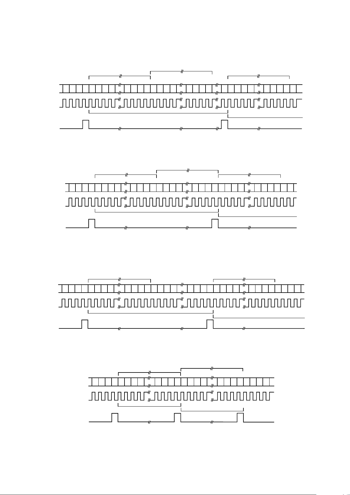
321015141312
321015141312
321015141312
321015141312
512 BITS
MSB
MSB
MSB
MSB
512 BITS
256 BITS 256 BITS
SLOT 15SLOT 0
SLOT 15SLOT 0
SLOT 31 SLOT 16
SLOT 16
256 BITS
256 BITS
SAMPLE PERIOD N
SAMPLE PERIOD N+1
SAMPLE PERIOD N+2
SAMPLE
PERIOD N+3
FRAME M
FRAME M+1
SDI OR SDO
SCLK
SDFS
FRS = 0 [DEFAULT 32 SLOTS PER FRAME, 2 SAMPLES PER FRAME SYNC]
MASTER MODE
NOTE THAT AD1843 FRAME RATE IS NOT RELATED TO SAMPLE RATES
Figure 7. FRS = 0, Master Mode Timing
321015141312
321015141312
321015141312
321015141312
256 BITS
MSB
MSB
MSB
MSB
256 BITS
SLOT 15SLOT 0
SLOT 15SLOT 0
SLOT 15 SLOT 0
SLOT 0
SAMPLE PERIOD N
SAMPLE PERIOD N+1
SAMPLE PERIOD N+2
SAMPLE
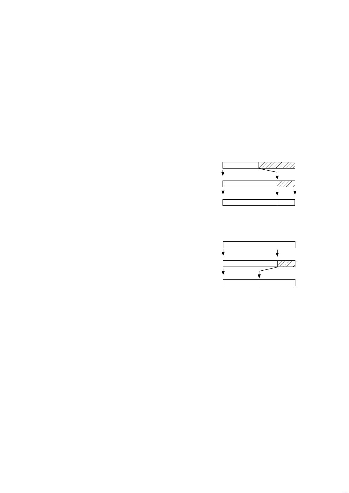
PERIOD N+3
FRAME M
SDI OR SDO
SCLK
SDFS
FRS = 1 [16 SLOTS PER FRAME, 1 SAMPLE PER FRAME SYNC]
MASTER MODE
NOTE THAT SCLK CAN BE PROGRAMMED FOR EITHER 12.288 MHz
OR 16.384 MHz WHEN IN MASTER MODE
256 BITS
FRAME M+1
FRAME M+2
FRAME M+3
Figure 8. FRS = 1, Master Mode Timing
Page 18
REV. 0–18–
AD1843
15 14 13 12
321015141312
3210 15141312 321015
512 BITS
MSB
MSB
MSB
MSB
512 BITS
256 BITS
256 BITS
SLOT 15SLOT 0
SLOT 15SLOT 0
SLOT 31 SLOT 16
256 BITS
SAMPLE PERIOD N
SAMPLE PERIOD N+1
SAMPLE PERIOD N+2
FRAME M
FRAME M+1
SDI OR SDO
SCLK
TSI
FRS = 0 [DEFAULT 32 SLOTS PER FRAME, 2 SAMPLES PER FRAME SYNC]
EXAMPLE SHOWING GAPS BETWEEN FRAMES
SLAVE MODE
GAP
GAP
Figure 9a. FRS = 0, Slave Mode Timing
321015141312
512 BITS
MSB
MSB
MSB
MSB
512 BITS
256 BITS
256 BITS
SLOT 15SLOT 0
SLOT 15SLOT 0
SLOT 31 SLOT 16
256 BITS
SAMPLE PERIOD N
SAMPLE PERIOD N+1
SAMPLE PERIOD N+2
FRAME M
FRAME M+1
SDI OR SDO
SCLK
TSI
FRS = 0 [DEFAULT 32 SLOTS PER FRAME, 2 SAMPLES PER FRAME SYNC]
EXAMPLE SHOWING NO GAPS BETWEEN FRAMES
SLAVE MODE
321015141312
321015141312
32101514
Figure 9b. FRS = 0, Slave Mode Timing
FRS = 1 [16 SLOTS PER FRAME, 1 SAMPLES PER FRAME SYNC]
EXAMPLE SHOWING GAPS BETWEEN FRAMES
SLAVE MODE
GAPGAP
15 14 13 12
3210
15 14 13 12
3210
256 BITS
MSBMSB
256 BITS
SLOT 15SLOT 0
SLOT 15SLOT 0
SAMPLE PERIOD N SAMPLE PERIOD N+1
FRAME M
FRAME M+1
SDI OR SDO
SCLK
TSI
GAP
Figure 10a. FRS = 1, Slave Mode Timing
FRS = 1 [16 SLOTS PER FRAME, 1 SAMPLES PER FRAME SYNC]
EXAMPLE SHOWING NO GAPS BETWEEN FRAMES
SLAVE MODE
15 14 13 12
3210
15 14 13 12
3210
256 BITS
MSBMSB
256 BITS
SLOT 15SLOT 0
SLOT 15SLOT 0
SAMPLE PERIOD N
SAMPLE PERIOD N+1
FRAME M
FRAME M+1
SDI OR SDO
SCLK
TSI
3210 15 14 13 12
MSB
Figure 10b. FRS = 1, Slave Mode Timing
Page 19

AD1843
REV. 0 –19–
Modem Data Access Arrangement (DAA) devices are generally
differential on the transmit side, and single-ended on the receive
side. The DAA transmit input (generally differential) should be
connected to the DAC2 output, pins LOUT2LP and LOUT2LN,
or LOUT2RP and LOUT2RN. The DAA receive output
(generally single-ended) should be connected to one of the
ADC line inputs, LINLP or LINRP. See the “APPLICATION
CIRCUITS” section below for more detail on the electrical
connections. There are several software driver steps that are required to configure the SoundComm codec for use as a modem
AFE.
Configure DAC2
1. Set the DA2FLT bit (Control Register Address 25, Bit 9) to
“1,” to select the digital modem filter mode. The DAC2 outputs can be used either as differential outputs or single-ended
outputs depending on how the pins are connected electrically;
no Control Register writes are required to configure the DAC2
outputs as either differential or single-ended.
2. Program LDA2G5:0 (Control Register Address 10, Bits 8
through 13) to “00 0101” (i.e., +4.5 dB) or RDA2G5:0
(Control Register 10, Bits 0 through 5) to “00 0101” (i.e.,
+4.5 dB), depending on whether the DAA transmit input is
connected to the left channel DAC2 output (use LDA2G5:0)
or the right channel DAC2 output (use RDA2G5:0). This
code establishes the DAC2 nominal analog output swing at
3.156 V p-p single-ended, or 6.312 V p-p differentially. The
3.156 V p-p level is equivalent to 3.17 dBm.
Configure ADC
1. Set the ADLFLT bit (Control Register Address 25, Bit 0) to
“1,” or the ADRFLT bit (Control Register Address 25, Bit 1)
to “1,” to select the digital modem filter mode. Set ADLFLT
if the DAA receive output is connected to the AD1843
LINLP input; set ADRFLT if the DAA receive output is
connected to the AD1843 LINRP input. Set the LINLSD bit
(Control Register Address 28, Bit 0) to “1” if the DAA is
connected to the AD1843 LINLP input; set the LINRSD bit
(Control Register Address 28, Bit 1) to “1” if the DAA is
connected to the AD1843 LINRP input.
2. Program LIG3:0 (Control Register Address 2, Bits 8 through
11) to “0000” (i.e., 0.0 dB) or RIG3:0 (Control Register
Address 2, Bits 0 through 3) to “0000” (i.e., 0.0 dB) depending on whether the left or right ADC input channel is
being used for the modem function. This code maps an analog input swing of 3.156 V p-p to the full dynamic range of
the 16-bit digital sample (i.e., ± 2
15
). The 3.156 V p-p level is
equivalent to 3.17 dBm.
Note that if the AD1843 is to be reconfigured dynamically, the
affected converter must be powered down before its associated
digital filter can be changed. In other words, if the digital filter
for the ADC left channel is being changed from audio mode to
modem mode, the ADC left channel must be powered down
first (using the ADLEN bit in Control Register Address 27).
Use the ADREN bit in Control Register Address 27 for the
ADC right channel, the DAC1EN bit in Control Register
Address 27 for DAC1, and the DAC2EN bit in Control Register Address 27 for DAC2.
Typical Configurations
Figure 6 below illustrates example connections between the
AD1843 SoundComm codec and other system resources. The
rich analog input and output connectivity of the AD1843 allows
a wide variety of configuration possibilities. Note that the level
of modem, speakerphone and external speaker concurrency is
application and DSP resource dependent.
SERIAL INTERFACE
The AD1843 SoundComm Codec transmits and receives both
data and control/status information through its serial port.
The AD1843 can be configured as either master or slave of the
serial interface. This is selected by using the BM pin. When
BM is tied HI, the AD1843 serves as bus master and supplies
the frame sync and the serial clock. When BM is tied LO, the
AD1843 serves as bus slave and receives the frame sync and the
serial clock. The level on BM should not be altered unless the
reset pin (
RESET) is asserted.
The AD1843 has six pins devoted to the serial interface: SDI,
SDO, SCLK, SDFS, TSI and TSO. The SDI pin is for serial
data input to the AD1843 and the SDO pin is for serial data
output from the AD1843. The SCLK pin is the serial interface
clock. Communication in and out of the AD1843 requires bits
of data to be transmitted after a rising edge of SCLK, and
sampled on a falling edge of SCLK. When the AD1843 is bus
master (BM pin tied HI), the SCLK frequency driven by the
AD1843 will be 12.288 MHz by default, but this can be increased to 16.384 MHz by setting the SCF bit in Control Register 26. When the AD1843 is bus slave (BM pin tied LO), the
SCLK frequency driven to the AD1843 may be as high as
24.576 MHz, but must not be any higher than the frequency on
the XTALI pin.
The SDFS pin is for the serial interface frame sync. When bus
master, new frames are marked by a HI pulse driven out on
SDFS one serial clock period before the frame begins. When
bus slave, new frames must be marked by a LO to HI transition
driven in on SDFS one serial clock period before the frame begins, but the transition back from HI to LO may occur at any
time provided the HI and LO times of SDFS are at least one
SCLK period in duration each.
When the AD1843 is bus master, frame size is controlled by the
FRS bit in Control Register 26. When FRS is set to “1,” each
frame is divided into 16 slots of 16 bits. When FRS is reset to
“0,” each frame is divided into 32 slots of 16 bits. In 32 slot
configuration, the second 16 slots of a frame must have slot assignments that are identical to the first 16 slots of the frame; 32
slot configuration is essentially 16 slot configuration with every
other SDFS pulse missing. Although these are the frame sizes
Page 20

REV. 0–20–
AD1843
for Control Register write data input and read data output. The
remaining slots are used for playback (DAC) data input and
capture (ADC) data output, where each channel has an assigned
slot. Table II and Figure 11 illustrate these slot assignments.
Since the conversion channels of the AD1843 can be programmed to run at different sample rates, a communication
mechanism indicates when playback channels request data,
when playback data is actually sent to the AD1843, and when
transmission of capture data from the AD1843 becomes necessary. This is facilitated by the Control and Status Words located in the first slot. The Control Word indicates which slots
in the current frame contain valid playback data. The Status
Word indicates if playback data can be sent to the AD1843 during the next frame, and which slots in the current frame contain
valid capture data. See the descriptions of the Control Word
and the Status Word below for additional detail.
Four word FIFO buffers are used on the inputs of each of the
DACs to allow data to be transferred in small bursts. This reduces the required response time to playback data requests, and
also buffers differences between the frame sync rate and the
channel sample rate. The Status Word indicates that playback
data can be sent if there is any room in the buffers, thus tending
to keep the input buffers full. Underrun flags are available in
Control Register 1, which indicate if an input buffer ran out of
data. If an underrun occurs, a zero is used in place of the unavailable data. To ensure underruns do not occur, playback data
must be sent to the AD1843 within two sample periods after the
status word indicates that the DAC FIFO is not full.
Note that the DAC Not Full status bits (DA2RQ and DA1RQ
in the Status Word Output) are updated immediately (i.e., in
the same frame as a valid write to the DAC FIFOs). If the DAC
Input Valid Flags (DA2V and DA1V in the Control Word
Input) are set (i.e., DAC data is valid) and only one location in
the DAC1 and DAC2 input FIFOs is available, then the
DA2RQ and DA1RQ status bits will reflect this valid write, and
will be reset to “0.” This is possible because the DA2V and
DA1V bits are in the most significant bits of the Control Word
and the DA2RQ and DA1RQ bits are in the least significant bits
of the Status Word, and the AD1843 uses this intervening time
Table II. AD1843 Slot Assignment
32 Slot Mode (FRS Reset to “0”)
Slot SDI Pin SDO Pin
0 & 16 Control Word Input Status Word Output
1 & 17 Control Register Data Input Control Register Data Output
2 & 18 Playback Data Input—DAC1 Left Capture Data Output—ADC Left
3 & 19 Playback Data Input—DAC1 Right Capture Data Output—ADC Right
4 & 20 Playback Data Input—DAC2 Left Reserved (Unused)
5 & 21 Playback Data Input—DAC2 Right Reserved (Unused)
16 Slot Mode (FRS Set to “1”)
Slot SDI Pin SDO Pin
0 Control Word Input Status Word Output
1 Control Register Data Input Control Register Data Output
2 Playback Data Input—DAC1 Left Capture Data Output—ADC Left
3 Playback Data Input—DAC1 Right Capture Data Output—ADC Right
4 Playback Data Input—DAC2 Left Reserved (Unused)
5 Playback Data Input—DAC2 Right Reserved (Unused)
produced by an AD1843 serving as bus master, an AD1843
serving as bus slave does not actually require these frame sizes.
When FRS is set to “1,” a slave will operate correctly with any
number or fraction of slots, provided there are enough slots for
it to complete its necessary communication (see below). When
FRS is reset to “0,” a slave can also operate correctly with a
wide range in the number of slots per frame, however it will automatically retake ownership of the serial interface bus 16 slots
after it is first given ownership of the bus in a frame.
The nominal minimum number of slots when the AD1843 is
configured in slave mode is six. The codec must be supplied
with at least 6 × 16 = 96 SCLK periods (both rising and falling
edges); SCLK may be gated (i.e., no need to be continuous)
between valid slots.
While SDFS marks the beginning of frames, AD1843 bus ownership during a frame is controlled by the TSI (Time Slot In)
and TSO (Time Slot Out) pins. When bus slave, a level HI on
TSI grants the AD1843 bus ownership beginning with the next
SCLK period. The TSI pin is monitored only when an AD1843
does not already own the bus; once an AD1843 is given ownership of the bus, the level on TSI is ignored until one SCLK
period before bus ownership is relinquished. Bus ownership will
last for six slots. Coincident with the final SCLK period of the
final slot owned, the AD1843 asserts TSO HI. This allows
chaining of AD1843s onto a common serial bus by connecting
the TSO pin of one AD1843 to the TSI pin on the next later
AD1843 in a chain. In single codec systems where the
SoundComm is configured as bus slave, connect the AD1843
SDFS and TSI signals together. When an AD1843 is bus master, its function is identical to that just described for the slave,
except a bus master always owns the first six slots and its TSI
pin is ignored (but should be tied LO).
Whenever an AD1843 does not own the bus, its SDO pin will
be three-stated and its SDI pin is ignored. Figures 7 through 10
illustrate the signal, slot, sample and frame relationships for the
four basic operating modes of the AD1843 serial interface.
The AD1843 requires slots of communication each time it takes
ownership of the serial bus. The first slot is used for a Control
Word input and a Status Word output. The second slot is used
Page 21

AD1843
REV. 0 –21–
interval to update the DAC Not Full status bits. Therefore
driver software does not have to make provision for frame-toframe delays between control and status information; the information in each frame is always up to date.
The AD1843 supports locking to an external clock which may
result in a sample rate that is marginally higher than the nominal
audio standard maximum sample rate of 48 kHz. This is necessary since two crystal-based clock sources are never perfectly
matched to one another. One is always at a slightly higher frequency. The AD1843 conversion channels have been designed
to support sample rates that are up to 2.1% higher than 48 kHz
(i.e., 49 kHz), referenced to the AD1843’s clock input on
XTALI, when all conversion channels are simultaneously running. Even higher rates can be supported when all channels are
not running simultaneously. See the “Conversion Rates” section above for additional details. The serial interface must also
allow for this higher sample rate with a frame sync (SDFS) rate
that is at least as high as the sample rate in 16 slot per frame
mode, or half as high as the sample rate in 32 slot per frame
mode. When the AD1843 is bus master, the SCLK frequency
is either 12.288 MHz or 16.384 MHz, which allows for up to
48 kHz or 64 kHz sampling rates, respectively.
The AD1843 Control Registers are read and written by transmitting a read/write request bit along with the Control Register
address in the slot 0 Control Word. When a read is requested,
the contents of the Control Register addressed is transmitted
out during slot 1 of the following frame. When a write is requested, data to be written must be transmitted to the AD1843
in slot 1, and the former contents of the control register are
transmitted out during slot 1 of the following frame. Unless otherwise noted, Control Register writes do not take effect until the
current round of six communication TDM time slots concludes.
Equivalently, unless otherwise noted, Control Register writes do
not take effect until the subsequent falling edge of the TSO signal.
The following sections describe the bit assignments for all time
slots.
IGNORED
3-STATED
CONTROL WORD
STATUS WORD
REGISTER DATA
REGISTER DATA
DAC1 LEFT
ADC LEFT
DAC1 RIGHT
ADC RIGHT
DAC2 LEFT0sDAC2 RIGHT
0s
IGNORED
3-STATED
SDI
SDO
16-BIT
STEREO
DON'T
CARE
IGNORED
3-STATED
CONTROL WORD
STATUS WORD
REGISTER DATA
REGISTER DATA
IGNORED
3-STATED
0s
DAC1R
DON'T
CARE
DAC2L
DAC2R
DON'T
CARE
0s
DAC1L
DON'T
CARE
0s0sADCL
ADCR
SDI
SDO
8-BIT
STEREO
IGNORED
3-STATED
CONTROL WORD
STATUS WORD
REGISTER DATA
REGISTER DATA
DAC1
ADC LEFT
DON'T CARE
ADC RIGHT
DAC2
0s
DON'T CARE
0s
IGNORED
3-STATED
SDI
SDO
16-BIT
MONO
DAC1, DAC2
IGNORED
3-STATED
CONTROL WORD
STATUS WORD
REGISTER DATA
REGISTER DATA
DON'T CARE DON'T CARE
0s
DAC2
0s
DON'T
CARE
0s
DON'T
CARE
0s
DAC1
ADCL ADCR
IGNORED
3-STATED
SDI
SDO
8-BIT
MONO
DAC1, DAC2
THE DIAGRAM ABOVE IS INTENDED TO BE ILLUSTRATIVE OF THE MORE COMMONLY USED CONFIGURATIONS. ADC LEFT, ADC RIGHT, DAC1
AND DAC2 CAN BE INDIVIDUALLY ASSIGNED TO 8-BIT OR 16-BIT SAMPLE WIDTH, AND DAC1 AND DAC2 CAN BE INDIVIDUALLY ASSIGNED
TO STEREO OR MONO MODE. EACH AD1843 CONSUMES 6 TMD SLOTS (REQUIRING 96 SCLK PERIODS), LEAVING 10 TDM SLOTS
UNUSED IN A 16 SLOT FRAME.
NOTE THAT BECAUSE THE SERIAL INTERFACE AND THE ADC AND DACS ARE IN GENERAL ASYNCHRONOUS, NOT EVERY CAPTURE OR
PLAYBACK TIME SLOT WILL CONTAIN VALID DATA. THE HOST PROCESSOR MUST POLL THE STATUS WORD TO DETERMINE WHETHER
THE ADC DATA IS VALID AND WHETHER THE DAC IS REQUESTING ADDITIONAL SAMPLES.
TIME
SLOT 0
TIME
SLOT 1
TIME
SLOT 2
TIME
SLOT 3
TIME
SLOT 4
TIME
SLOT 5
SCLK
SDFS
16 BITS
Figure 11. AD1843 Slot Assignments
Page 22

REV. 0–22–
AD1843
SERIAL INTERFACE INPUT
Note that the references to slot numbers are valid only when the AD1843 is configured in master mode. For slave mode, bus ownership does not necessarily start on Slot 0.
Control Word Input (Slot 0 or 16)
Data 15 Data 14 Data 13 Data 12 Data 11 Data 10 Data 9 Data 8
res res res res res res DA2V DA1V
Data 7 Data 6 Data 5 Data 4 Data 3 Data 2 Data 1 Data 0
R/W res res IA4 IA3 IA2 IA1 IA0
DA2V DAC2 Input Valid Flag. When in DAC2 stereo mode, setting this bit to “1” indicates that slots 4 and 5
contain valid playback data for the left and right channels of DAC2, respectively. When in DAC2 mono
mode, setting this bit to “1” indicates that slot 4 contains valid playback data for both left and right channels
of DAC2. Slot 5 is ignored in DAC2 mono mode. When this bit is reset to “0,” data in slots 4 and 5 is
ignored. This bit is ignored if the AD1843 did not request data for DAC2 in the last frame (see the DA2RQ
bit in the Status Word Output).
DA1V DAC1 Input Valid Flag. When in DAC1 stereo mode, setting this bit to “1” indicates that slots 2 and 3
contain valid playback data for the left and right channels of DAC1, respectively. When in DAC1 mono
mode, setting this bit to “1” indicates that slot 2 contains valid playback data for both left and right channels
of DAC1. Slot 3 is ignored in DAC1 mono mode. When this bit is reset to “0,” data in slots 2 and 3 is
ignored. This bit is ignored if the AD1843 did not request data for DAC1 in the last frame (see the DA1RQ
bit in the Status Word Output).
R/W Read/Write Request. Either a read from or a write to a Control Register occurs every frame. Setting this bit
to “1” indicates a Control Register read while resetting this bit to “0” initiates a Control Register write. Bits
IA4:0 define the Control Register address. When reading, the contents of the Control Register addressed are
transmitted during slot 1 of the following frame. When writing, the data to be written is taken from slot 1
and the former contents of the Control Register are transmitted during slot 1 of the following frame.
IA4:0 Control Register address for read or write.
res Reserved for future expansion. To ensure future compatibility, write “0” to all reserved bits.
Control Register Write Data Input (Slot 1 or 17)
Data 15 Data 14 Data 13 Data 12 Data 11 Data 10 Data 9 Data 8
DATA15 DATA14 DATA13 DATA12 DATA11 DATA10 DATA9 DATA8
Data 7 Data 6 Data 5 Data 4 Data 3 Data 2 Data 1 Data 0
DATA7 DATA6 DATA5 DATA4 DATA3 DATA2 DATA1 DATA0
Format for the input data to written to the addressed Control Register. MSB is first.
DAC1 Left Sample Input (Slot 2 or 18)
Data 15 Data 14 Data 13 Data 12 Data 11 Data 10 Data 9 Data 8
DATA15 DATA14 DATA13 DATA12 DATA11 DATA10 DATA9 DATA8
Data 7 Data 6 Data 5 Data 4 Data 3 Data 2 Data 1 Data 0
DATA7 DATA6 DATA5 DATA4 DATA3 DATA2 DATA1 DATA0
Data format may be 8-bit unsigned linear PCM, 16-bit signed linear PCM, 8-bit µ-Law companded, or 8-bit A-Law companded.
MSB is first. DATA7:0 are ignored in 8-bit linear or 8-bit companded modes.
Page 23

AD1843
REV. 0 –23–
DAC1 Right Sample Input (Slot 3 or 19)
Data 15 Data 14 Data 13 Data 12 Data 11 Data 10 Data 9 Data 8
DATA15 DATA14 DATA13 DATA12 DATA11 DATA10 DATA9 DATA8
Data 7 Data 6 Data 5 Data 4 Data 3 Data 2 Data 1 Data 0
DATA7 DATA6 DATA5 DATA4 DATA3 DATA2 DATA1 DATA0
Data format may be 8-bit unsigned linear PCM, 16-bit signed linear PCM, 8-bit µ-Law companded, or 8-bit A-Law companded.
MSB is first. DATA7:0 are ignored in 8-bit linear or 8-bit companded modes.
DAC2 Left Sample Input (Slot 4 or 20)
Data 15 Data 14 Data 13 Data 12 Data 11 Data 10 Data 9 Data 8
DATA15 DATA14 DATA13 DATA12 DATA11 DATA10 DATA9 DATA8
Data 7 Data 6 Data 5 Data 4 Data 3 Data 2 Data 1 Data 0
DATA7 DATA6 DATA5 DATA4 DATA3 DATA2 DATA1 DATA0
Data format may be 8-bit unsigned linear PCM, 16-bit signed linear PCM, 8-bit µ-Law companded, or 8-bit A-Law companded.
MSB is first. DATA7:0 are ignored in 8-bit linear or 8-bit companded modes.
DAC2 Right Sample Input (Slot 5 or 21)
Data 15 Data 14 Data 13 Data 12 Data 11 Data 10 Data 9 Data 8
DATA15 DATA14 DATA13 DATA12 DATA11 DATA10 DATA9 DATA8
Data 7 Data 6 Data 5 Data 4 Data 3 Data 2 Data 1 Data 0
DATA7 DATA6 DATA5 DATA4 DATA3 DATA2 DATA1 DATA0
Data format may be 8-bit unsigned linear PCM, 16-bit signed linear PCM, 8-bit µ-Law companded, or 8-bit A-Law companded.
MSB is first. DATA7:0 are ignored in 8-bit linear or 8-bit companded modes.
Page 24

REV. 0–24–
AD1843
SERIAL INTERFACE OUTPUT
Status Word Output (Slot 0 or 16)
Data 15 Data 14 Data 13 Data 12 Data 11 Data 10 Data 9 Data 8
res res res res res res ADRV ADLV
Data 7 Data 6 Data 5 Data 4 Data 3 Data 2 Data 1 Data 0
res res res res res res DA2RQ DA1RQ
ADRV Right ADC Channel Output Valid Flag. Set to “1” if slot 3 (or 19) contains valid right ADC capture data.
ADLV Left ADC Channel Output Valid Flag. Set to “1” if slot 2 (or 18) contains valid left ADC capture data.
DA2RQ DAC2 Input Request Flag. Set to “1” if DAC2 is enabled and its four word stereo input buffer is not full.
DA1RQ DAC1 Input Request Flag. Set to “1” if DAC1 is enabled and its four word stereo input buffer is not full.
res Reserved for future expansion. Read back as “0.” Should be ignored to ensure future compatibility.
Control Register Data Output (Slots 1 or 17)
Data 15 Data 14 Data 13 Data 12 Data 11 Data 10 Data 9 Data 8
DATA15 DATA14 DATA13 DATA12 DATA11 DATA10 DATA9 DATA8
Data 7 Data 6 Data 5 Data 4 Data 3 Data 2 Data 1 Data 0
DATA7 DATA6 DATA5 DATA4 DATA3 DATA2 DATA1 DATA0
Contents of Control Register addressed in previous frame.
ADC Left Sample Output (Slots 2 or 18)
Data 15 Data 14 Data 13 Data 12 Data 11 Data 10 Data 9 Data 8
DATA15 DATA14 DATA13 DATA12 DATA11 DATA10 DATA9 DATA8
Data 7 Data 6 Data 5 Data 4 Data 3 Data 2 Data 1 Data 0
DATA7 DATA6 DATA5 DATA4 DATA3 DATA2 DATA1 DATA0
Data format may be 8-bit unsigned linear PCM, 16-bit signed linear PCM, 8-bit µ-Law companded, or 8-bit A-Law companded.
MSB is first. DATA7:0 are ignored in 8-bit linear or 8-bit companded modes.
ADC Right Sample Output (Slots 3 or 19)
Data 15 Data 14 Data 13 Data 12 Data 11 Data 10 Data 9 Data 8
DATA15 DATA14 DATA13 DATA12 DATA11 DATA10 DATA9 DATA8
Data 7 Data 6 Data 5 Data 4 Data 3 Data 2 Data 1 Data 0
DATA7 DATA6 DATA5 DATA4 DATA3 DATA2 DATA1 DATA0
Data format may be 8-bit unsigned linear PCM, 16-bit signed linear PCM, 8-bit µ-Law companded, or 8-bit A-Law companded.
MSB is first. DATA7:0 are ignored in 8-bit linear or 8-bit companded modes.
Page 25

AD1843
REV. 0 –25–
Reserved Output (Slots 4 or 20)
Data 15 Data 14 Data 13 Data 12 Data 11 Data 10 Data 9 Data 8
res res res res res res res res
Data 7 Data 6 Data 5 Data 4 Data 3 Data 2 Data 1 Data 0
res res res res res res res res
res Reserved for future expansion. Read back as “0.” Should be ignored to ensure future compatibility.
Reserved Output (Slots 5 or 21)
Data 15 Data 14 Data 13 Data 12 Data 11 Data 10 Data 9 Data 8
res res res res res res res res
Data 7 Data 6 Data 5 Data 4 Data 3 Data 2 Data 1 Data 0
res res res res res res res res
res Reserved for future expansion. Read back as “0.” Should be ignored to ensure future compatibility.
CONTROL REGISTERS
Control Register Architecture
All Control Registers are cleared to their default state when either the RESET pin or the PWRDWN pin is asserted. All conversion
related Control Registers (Addresses 1–15, 25 and 27) are cleared to defaults when the conversion resources of the AD1843 are powered down through the PDNI bit in Control Register Address 28. Control Registers which manage analog DAC gain/attenuation
(Addresses 3–10) are cleared to defaults whenever the resource they manage is powered down. Finally, the three clock generator
sample phase shift Control Registers (Addresses 18, 21 and 24) are cleared to defaults whenever their associated clock generator is
powered down. Writes to Control Registers are blocked until a clearing condition no longer exists. Writes to Control Registers are
also blocked immediately after the
RESET pin or the PWRDWN pin is asserted until the AD1843’s internal clocks have settled,
which is indicated by the INIT bit in Control Register Address 0. Control Registers may always be read.
Figures 12 and 13 associate the Control Registers to the AD1843 Block Diagram.
Page 26

REV. 0–26–
AD1843
4
CMOUT
V
REF
∑
HPOUTR
HPOUTC
HPOUTL
LOUT2LP
LOUT2LN
LOUT2RP
LOUT2RN
LEFT
RIGHT
20 dB
AUX3L
AUX2R
AUX1L
AUX2L
AUX1R
LINRP
LINRN
MICR
MICL
GN/AT = GAIN/
ATTENUATION
DRIVER
AD1843
AAFILTL
AAFILTR
SUML
SUMR
LINLP
LINLN
MOUT
∑
∑
∑
∑
∑
∑
∑
∑
∑
MUTE
MUTE
∑∆
DAC
MUTE
AUX3R
MIN
∑∆
ADC
PGA
VOLTAGE REFERENCE
CRA2
GN/AT
MUTE
CRA7
GN/AT
MUTE
CRA4
GN/AT
MUTE
CRA5
GN/AT
MUTE
CRA6
GN/AT
MUTE
CRA8
CRA8
CRA8
LOUT1L
LOUT1R
GN/AT
MUTE
CRA9
S
E
L
E
C
T
O
R
GN/AT
MUTE
CRA3
MUTE
CRA8
GN/AT
MUTE
CRA10
CRAX = CONTROL REGISTER ADDRESS “X”
GNDA
FILTRFILTL
CRA2
∑∆
DAC
Address Register Description
0 Codec Status and Revision Identification (Read Only)
1 Channel Status Flags
2 Input Control—ADC Source and Gain/Attenuation
3 Mix Control—DAC2 to Mixer
4 Mix Control—Auxiliary 1 to Mixer
5 Mix Control—Auxiliary 2 to Mixer
6 Mix Control—Auxiliary 3 to Mixer
7 Mix Control—Mic to Mixer
8 Mix/Misc. Control—Mono In to Mixer and Miscellaneous Settings
9 Output Control—DAC1 Analog Gain/Attenuation
10 Output Control—DAC2 Analog Gain/Attenuation
11 Output Control—DAC1 Digital Attenuation
12 Output Control—DAC2 Digital Attenuation
13 Digital Mix Control—ADC to DAC1
14 Digital Mix Control—ADC to DAC2
15 Codec Configuration—Channel Sample Rate Source Select
Figure 12. AD1843 Control Registers Associated with Block Diagram
Page 27

AD1843
REV. 0 –27–
8 9
GNDD
V
DD
S
E
L
E
C
T
O
R
2
LEFT
RIGHT
LEFT
RIGHT
3
V
CC
ADC
µ/A
LAW
D
I
G
I
T
A
L
I
N
T
E
R
F
A
C
E
CONTROL AND STATUS REGISTERS
CRA0, CRA1, CRA25, CRA26,
CRA27, CRA28
RESET
PWRDWN
∑
∑
MUTE
ATTN
∑
∑
MUTE
∑
∑
∑
∑
FIFO
S
E
L
E
C
T
O
R
µ/A
LAW
SCLK
SDFS
SDI
SDO
BM
CS
TSO
TSI
XCTL [1:0]
PDMNFT
CLOCK GENERATION
CLKOUT
XTALI
XTALO
SYNC3 SYNC2 SYNC1 CONV3 CONV2 CONV1 BIT3 BIT2 BIT1
CRA15, CRA16, CRA17, CRA18, CRA19,
CRA20, CRA21, CRA22, CRA23, CRA24
AD1843
CRAX = CONTROL REGISTER ADDRESS “X”
CRA25
CRA25
CRA25
CRA25
CRA12
CRA11
ATTN
MUTE
CRA13
ATTN
MUTE
CRA14
CRA26
CRA26
DAC1
DAC2
CRA26
µ/A
LAW
FIFO
ATTN
Address Register Description
16 Clock Generator 1 Control—Mode
17 Clock Generator 1 Control—Sample Rate
18 Clock Generator 1 Control—Sample Phase Shift
19 Clock Generator 2 Control—Mode
20 Clock Generator 2 Control—Sample Rate
21 Clock Generator 2 Control—Sample Phase Shift
22 Clock Generator 3 Control—Mode
23 Clock Generator 3 Control—Sample Rate
24 Clock Generator 3 Control—Sample Phase Shift
25 Codec Configuration—Digital Filter and Mode Select
26 Codec Configuration—Serial Interface
27 Codec Configuration—Channel Power Down
28 Codec Configuration—Fundamental Settings
29 Reserved for Future Expansion
30 Reserved for Future Expansion
31 Reserved for Future Expansion
Figure 13. AD1843 Control Registers Associated with Block Diagram
Page 28

REV. 0–28–
AD1843
Address 0 Codec Status and Revision Identification
Data 15 Data 14 Data 13 Data 12 Data 11 Data 10 Data 9 Data 8
INIT PDNO res res res res res res
Data 7 Data 6 Data 5 Data 4 Data 3 Data 2 Data 1 Data 0
res res res res ID3 ID2 ID1 ID0
This register is read only.
INIT Clock Initialization Flag. This bit is set to “1” if the AD1843’s internal clocks generated from the crystal input pin
XTALI have not yet stabilized. When set to “1,” Control Registers may be read if the AD1843 is configured as a Bus
Slave (see the definition for the BM pin), but Control Register writes will be blocked. This bit is set to a “1” after the
RESET pin is asserted, or when the power-down sequence (initiated by asserting the PWRDWN pin) has completed.
The bit is reset to “0” usually within 400 to 800 µsec after the
RESET or the PWRDWN pin is deasserted, depending
upon parasitic capacitance on the XTALI and XTALO pins outside the AD1843. Because these parasitics are a function of the board design and layout, the exact amount of time required for the crystal to start to oscillate, and the internal clocks to stabilize cannot be known exactly in advance.
PDNO Converter Power-Down Flag. This bit is set to “1” if the AD1843 conversion resources are powered down, or are in
the process of entering or exiting power down. Conversion resources are all resources in the AD1843 with the exception of the three clock generators and the serial interface. Conversion power-down is entered if either the power-down
pin (
PWRDWN) is driven LO, or if the PDNI (Converter Power Down) bit in Control Register Address 28 is as-
serted. Power down is exited only if both pin (
PWRDWN) and bit (PDNI) are deasserted. When this bit is set to
“1,” Control Registers may still be read, but only Control Registers 16–24, 26 and 28 which do not manage conversion resources may be written. See the “Power Management” section for further details. This bit is set to “1” immediately after a reset since the PDNI bit is initially asserted after a reset.
ID3:0 Revision Identification. These bits define the revision level of the AD1843. The first version of the AD1843 is
“0001.”
res Reserved for future expansion. To ensure future compatibility, write “0” to all reserved bits.
Initial default state after reset: 1100 0000 0000 0001 (C001 hex). Cleared to default and cannot be written to when:
the
RESET pin is asserted LO; or when the PWRDWN pin is asserted LO.
Address 1 Channel Status Flags
Data 15 Data 14 Data 13 Data 12 Data 11 Data 10 Data 9 Data 8
res res res res res res SU2 SU1
Data 7 Data 6 Data 5 Data 4 Data 3 Data 2 Data 1 Data 0
res res res res OVR1 OVR0 OVL1 OVL0
This register is cleared to all “0” after any read or write access.
SU2 DAC2 Sample Underrun. When set to “1,” this bit indicates that the four word stereo input buffer for DAC pair 2
ran out of samples. If this occurs, zeros are used in place of the unavailable data. This bit is “sticky” and is cleared
after any write to this register. It is also cleared by powering down DAC2 (see the DA2EN bit in Control Register
Address 27).
SU1 DAC1 Sample Underrun. When set to “1,” this bit indicates that the four word stereo input buffer for DAC pair 1
ran out of samples. If this occurs, zeros are used in place of the unavailable data. This bit is “sticky” and is cleared
after any write to this register. It is also cleared by powering down DAC1 (see the DA1EN bit in Control Register
Address 27).
OVR1:0 ADC Right Overrange Detect. These bits record the largest output magnitude on the ADC right channel and are
cleared to “00” after any write to this register. The peak amplitude as recorded by these bits is “sticky,” i.e., the largest output magnitude recorded by these bits will persist until these bits are explicitly cleared. They are also cleared by
powering down the ADC right channel (see the ADREN bit in Control Register Address 27).
00 = Greater than –1.0 dB underrange
01 = Between –1.0 dB and 0 dB underrange
10 = Between 0 dB and 1 dB overrange
11 = Greater than 1.0 dB overrange
Page 29

AD1843
REV. 0 –29–
OVL1:0 ADC Left Overrange Detect. These bits record the largest output magnitude on the ADC left channel and are
cleared to “00” after any write to this register. The peak amplitude as recorded by these bits is “sticky,” i.e., the largest output magnitude recorded by these bits will persist until these bits are explicitly cleared. They are also cleared by
powering down the ADC left channel (see the ADLEN bit in Control Register Address 27).
00 = Greater than –1.0 dB underrange
01 = Between –1.0 dB and 0 dB underrange
10 = Between 0 dB and 1 dB overrange
11 = Greater than 1.0 dB overrange
res Reserved for future expansion. To ensure future compatibility, write “0” to all reserved bits.
Initial default state after reset: 0000 0000 0000 0000 (0000 hex). Cleared to default when: the
RESET pin is asserted
LO; when the
PWRDWN pin is asserted LO; or when the PDNO bit in Control Register Address 0 is set to “1” (all
conversions disabled).
Address 2 Input Control—ADC Source and Gain/Attenuation
Data 15 Data 14 Data 13 Data 12 Data 11 Data 10 Data 9 Data 8
LSS2 LSS1 LSS0 LMGE LIG3 LIG2 LIG1 LIG0
Data 7 Data 6 Data 5 Data 4 Data 3 Data 2 Data 1 Data 0
RSS2 RSS1 RSS0 RMGE RIG3 RIG2 RIG1 RIG0
LSS2:0 Left ADC Source Select
000 = Left Line Input
001 = Left Mic Input
010 = Left Auxiliary 1 Input
011 = Left Auxiliary 2 Input
100 = Left Auxiliary 3 Input
101 = Mono Input
110 = Left DAC1 Output
111 = Left DAC2 Output
LMGE Left ADC Microphone Gain Enable
0 = 0 dB Gain
1 = +20 dB Gain
LIG3:0 Left ADC Input Gain. Least significant bit represents +1.5 dB.
0000 = 0.0 dB Gain
1111 = +22.5 dB Gain
RSS2:0 Right ADC Source Select
000 = Right Line Input
001 = Right Mic Input
010 = Right Auxiliary 1 Input
011 = Right Auxiliary 2 Input
100 = Right Auxiliary 3 Input
101 = Mono Input
110 = Right DAC1 Output
111 = Right DAC2 Output
RMGE Right ADC Microphone Gain Enable
0 = 0 dB Gain
1 = +20 dB Gain
RIG3:0 Right ADC Input Gain. Least significant bit represents +1.5 dB.
0000 = 0.0 dB Gain
1111 = +22.5 dB Gain
Initial Default State after Reset: 0000 0000 0000 0000 (0000 hex). Cleared to default and cannot be written to when:
the
RESET pin is asserted LO; when the PWRDWN pin is asserted LO; or when the PDNO bit in Control Register 0
is set to “1” (all conversions disabled).
Page 30

REV. 0–30–
AD1843
Address 3 Mix Control—DAC2 to Mixer
Data 15 Data 14 Data 13 Data 12 Data 11 Data 10 Data 9 Data 8
LD2MM res res LD2M4 LD2M3 LD2M2 LD2M1 LD2M0
Data 7 Data 6 Data 5 Data 4 Data 3 Data 2 Data 1 Data 0
RD2MM res res RD2M4 RD2M3 RD2M2 RD2M1 RD2M0
LD2MM Left DAC2 Mix Mute
0 = Mix Enabled
1 = Mix Muted
LD2M4:0 Left DAC2 Mix Gain/Attenuation Select. Least significant bit represents –1.5 dB. Referred to 2.0 V p-p DAC2
output level.
00000 = +12.0 dB Gain
01000 = 0.0 dB
11111 = –34.5 dB Attenuation
RD2MM Right DAC2 Mix Mute
0 = Mix Enabled
1 = Mix Muted
RD2M4:0 Right DAC2 Mix Gain/Attenuation Select. Least significant bit represents –1.5 dB. Referred to 2.0 V p-p DAC2
output level.
00000 = +12.0 dB Gain
01000 = 0.0 dB
11111 = –34.5 dB Attenuation
res Reserved for future expansion. To ensure future compatibility, write “0” to all reserved bits.
Initial default state after reset: 1000 1000 1000 1000 (8888 hex). Cleared to default and cannot be written to when:
the
RESET pin is asserted LO; when the PWRDWN pin is asserted LO; when the PDNO bit in Control Register
Address 0 is set to “1” (all conversions disabled); or when the DDMEN bit (DAC2 to DAC1 analog mix disabled),
the DA2EN bit (DAC2 powered down), or the ANAEN bit (analog channels powered down) in Control Register Address 27 is reset to “0.”
Address 4 Mix Control—Auxiliary 1 to DAC1
Data 15 Data 14 Data 13 Data 12 Data 11 Data 10 Data 9 Data 8
LX1MM res res LX1M4 LX1M3 LX1M2 LX1M1 LX1M0
Data 7 Data 6 Data 5 Data 4 Data 3 Data 2 Data 1 Data 0
RX1MM res res RX1M4 RX1M3 RX1M2 RX1M1 RX1M0
LX1MM Left Auxiliary 1 Mix Mute
0 = Mix Enabled
1 = Mix Muted
LX1M4:0 Left Auxiliary 1 Mix Gain/Attenuation Select. Least significant bit represents –1.5 dB. Referred to 2.0 V p-p DAC1
output level.
00000 = +12.0 dB Gain
01000 = 0.0 dB
11111 = –34.5 dB Attenuation
RX1MM Right Auxiliary 1 Mix Mute
0 = Mix Enabled
1 = Mix Muted
RX1M4:0 Right Auxiliary 1 Mix Gain/Attenuation Select. Least significant bit represents –1.5 dB. Referred to 2.0 V p-p DAC1
output level.
00000 = +12.0 dB Gain
01000 = 0.0 dB
11111 = –34.5 dB Attenuation
Page 31

AD1843
REV. 0 –31–
res Reserved for future expansion. To ensure future compatibility, write “0” to all reserved bits.
Initial default state after reset: 1000 1000 1000 1000 (8888 hex). Cleared to default and cannot be written
to when: the
RESET pin is asserted LO; when the PWRDWN pin is asserted LO; when the PDNO bit in
Control Register Address 0 is set to “1” (all conversions disabled); or when the AAMEN bit (analog input to
analog mix disabled), or the ANAEN bit (analog channels powered down) in Control Register Address 27 is
reset to “0.”
Address 5 Mix Control—Auxiliary 2 to Mixer
Data 15 Data 14 Data 13 Data 12 Data 11 Data 10 Data 9 Data 8
LX2MM res res LX2M4 LX2M3 LX2M2 LX2M1 LX2M0
Data 7 Data 6 Data 5 Data 4 Data 3 Data 2 Data 1 Data 0
RX2MM res res RX2M4 RX2M3 RX2M2 RX2M1 RX2M0
LX2MM Left Auxiliary 2 Mix Mute
0 = Mix Enabled
1 = Mix Muted
LX2M4:0 Left Auxiliary 2 Mix Gain/Attenuation Select. Least significant bit represents –1.5 dB. Referred to
2.0 V p-p DAC1 output level.
00000 = +12.0 dB Gain
01000 = 0.0 dB
11111 = –34.5 dB Attenuation
RX2MM Right Auxiliary 2 Mix Mute
0 = Mix Enabled
1 = Mix Muted
RX2M4:0 Right Auxiliary 2 Mix Gain/Attenuation Select. Least significant bit represents –1.5 dB. Referred to
2.0 V p-p DAC1 output level.
00000 = +12.0 dB Gain
01000 = 0.0 dB
11111 = –34.5 dB Attenuation
res Reserved for future expansion. To ensure future compatibility, write “0” to all reserved bits.
Initial default state after reset: 1000 1000 1000 1000 (8888 hex). Cleared to default and cannot be written to when:
the
RESET pin is asserted LO; when the PWRDWN pin is asserted LO; when the PDNO bit in Control Register Ad-
dress 0 is set to “1” (all conversions disabled); or when the AAMEN bit (analog input to analog mix disabled), or the
ANAEN bit (analog channels powered down) in Control Register Address 27 is reset to “0.”
Address 6 Mix Control—Auxiliary 3 to Mixer
Data 15 Data 14 Data 13 Data 12 Data 11 Data 10 Data 9 Data 8
LX3MM res res LX3M4 LX3M3 LX3M2 LX3M1 LX3M0
Data 7 Data 6 Data 5 Data 4 Data 3 Data 2 Data 1 Data 0
RX3MM res res RX3M4 RX3M3 RX3M2 RX3M1 RX3M0
LX3MM Left Auxiliary 3 Mix Mute
0 = Mix Enabled
1 = Mix Muted
LX3M4:0 Left Auxiliary 3 Mix Gain/Attenuation Select. Least significant bit represents –1.5 dB. Referred to
2.0 V p-p DAC1 output level.
00000 = +12.0 dB Gain
01000 = 0.0 dB
11111 = –34.5 dB Attenuation
Page 32

REV. 0–32–
AD1843
RX3MM Right Auxiliary 3 Mix Mute
0 = Mix Enabled
1 = Mix Muted
RX3M4:0 Right Auxiliary 3 Mix Gain/Attenuation Select. Least significant bit represents –1.5 dB. Referred to
2.0 V p-p DAC1 output level.
00000 = +12.0 dB Gain
01000 = 0.0 dB
11111 = –34.5 dB Attenuation
res Reserved for future expansion. To ensure future compatibility, write “0” to all reserved bits.
Initial default state after reset: 1000 1000 1000 1000 (8888 hex). Cleared to default and cannot be written to when:
the
RESET pin is asserted LO; when the PWRDWN pin is asserted LO; when the PDNO bit in Control Register
Address 0 is set to “1” (all conversions disabled); or when the AAMEN bit (analog input to analog mix disabled), or
the ANAEN bit (analog channels powered down) in Control Register Address 27 is reset to “0.”
Address 7 Mix Control—Mic to Mixer
Data 15 Data 14 Data 13 Data 12 Data 11 Data 10 Data 9 Data 8
LMCMM res res LMCM4 LMCM3 LMCM2 LMCM1 LMCM0
Data 7 Data 6 Data 5 Data 4 Data 3 Data 2 Data 1 Data 0
RMCMM res res RMCM4 RMCM3 RMCM2 RMCM1 RMCM0
LMCMM Left Microphone Mix Mute
0 = Mix Enabled
1 = Mix Muted
LMCM4:0 Left Microphone Mix Gain/Attenuation Select. Least significant bit represents –1.5 dB. Referred to 2.0 V p-p
DAC1 output level.
00000 = +12.0 dB Gain
01000 = 0.0 dB
11111 = –34.5 dB Attenuation
RMCMM Right Microphone Mix Mute
0 = Mix Enabled
1 = Mix Muted
RMCM4:0 Right Microphone Mix Gain/Attenuation Select. Least significant bit represents –1.5 dB. Referred to 2.0 V p-p
DAC1 output level.
00000 = +12.0 dB Gain
01000 = 0.0 dB
11111 = –34.5 dB Attenuation
res Reserved for future expansion. To ensure future compatibility, write “0” to all reserved bits.
Initial default state after reset: 1000 1000 1000 1000 (8888 hex). Cleared to default and cannot be written to when:
the
RESET pin is asserted LO; when the PWRDWN pin is asserted LO; when the PDNO bit in Control Register
Address 0 is set to “1” (all conversions disabled); or when the AAMEN bit (analog input to analog mix disabled), or
the ANAEN bit (analog channels powered down) in Control Register Address 27 is reset to “0.”
Address 8 Mix/Miscellaneous Control—Mono In to Mixer and Miscellaneous Settings
Data 15 Data 14 Data 13 Data 12 Data 11 Data 10 Data 9 Data 8
MNMM res res MNM4 MNM3 MNM2 MNM1 MNM0
Data 7 Data 6 Data 5 Data 4 Data 3 Data 2 Data 1 Data 0
ALLMM MNOM HPOM HPOS SUMM res DAC2T DAC1T
MNMM Mono Input Mix Mute
0 = Mix Enabled
1 = Mix Muted
Page 33

AD1843
REV. 0 –33–
MNM4:0 Left and Right Mono Mix Gain/Attenuation Select. Least significant bit represents –1.5 dB.
00000 = +12.0 dB Gain
01000 = 0.0 dB
11111 = –34.5 dB Attenuation
ALLMM All Mix Mute. Mutes all mixing (MIC, AUX1, AUX2, AUX3, and DAC2) to left and right DAC1, overriding the
independent mute control bits in Control Register Addresses 3 through 8.
0 = Mix to DAC1 Enabled
1 = Mix to DAC1 Muted
MNOM Mono Output Mute
0 = Mono Output Enabled
1 = Mono Output Muted
HPOM Headphone Output Mute (Left and Right)
0 = Headphone Output Enabled
1 = Headphone Output Muted
HPOS Headphone Output Voltage Swing (Left and Right)
0 = 2 volts peak-to-peak
1 = 4 volts peak-to-peak
SUMM Sum Left and Right Mute. Mutes mixing from SUML and SUMR pins to DAC1.
0 = SUML and SUMR Mix to DAC1 Enabled
1 = SUML and SUMR Mix to DAC1 Muted
DAC2T DAC2 Gain/Attenuation Change Timing. This bit controls when changes to the DAC2 gain/attenuation setting
(Control Register 10) take effect. When set to “1,” changes take effect immediately. When reset to “0,” changes are
delayed until either the output level on DAC2 crosses zero (midscale), or until after a 10 to 12 ms time-out period is
reached. Delaying gain/attenuation changes until zero crossings reduces instantaneous output voltage changes, which
reduces audible “clicks.”
0 = Gain/Attenuation Changes Applied on Signal Zero Crossing or After a 10-12 ms Time-Out
1 = Gain/Attenuation Changes Applied Immediately
DAC1T DAC1 Gain/Attenuation Change Timing. This bit controls when changes to the DAC1 gain/attenuation setting
(Control Register 9) take effect. When set to “1,” changes take effect immediately. When reset to “0,” changes are
delayed until either the output level on DAC1 crosses zero (midscale), or until after a 10 to 12 ms time-out period is
reached. Delaying gain/attenuation changes until zero crossings reduces instantaneous output voltage changes, which
reduces audible “clicks.”
0 = Gain/Attenuation Changes Applied on Signal Zero Crossing or After a 10-12 ms Time-Out
1 = Gain/Attenuation Changes Applied Immediately
res Reserved for future expansion. To ensure future compatibility, write “0” to all reserved bits.
Initial default state after reset: 1000 1000 0110 1000 (8868 hex). Cleared to default and cannot be written to when:
the
RESET pin is asserted LO; when the PWRDWN pin is asserted LO; or when the PDNO bit in Control Register
Address 0 is set to “1” (all conversions powered down). The MSB half (Data 15 through Data 8) of this Control Register is cleared to default and cannot be written to also when: the AAMEN bit (analog input to analog mix disabled),
or the ANAEN bit (analog channels powered down) in Control Register 27 is reset to “0.”
Address 9 Output Control—DAC1 Analog Gain/Attenuation
Data 15 Data 14 Data 13 Data 12 Data 11 Data 10 Data 9 Data 8
LDA1GM res LDA1G5 LDA1G4 LDA1G3 LDA1G2 LDA1G1 LDA1G0
Data 7 Data 6 Data 5 Data 4 Data 3 Data 2 Data 1 Data 0
RDA1GM res RDA1G5 RDA1G4 RDA1G3 RDA1G2 RDA1G1 RDA1G0
LDA1GM Left DAC1 Analog Mute
0 = Left DAC1 Enabled
1 = Left DAC1 Muted
Page 34

REV. 0–34–
AD1843
LDA1G5:0 Left DAC1 Analog/Digital Gain/Attenuation Select. Least significant bit represents –1.5 dB. Note that the
implementation of the attenuation is mixed analog and digital.
0 00000 = +12.0 dB: +12.0 dB Analog, +0.0 dB Digital
0 01000 = 0.0 dB: +0.0 dB Analog, +0.0 dB Digital
0 11111 = –34.5 dB: –34.5 dB Analog, +0.0 dB Digital
1 00000 = –36.0 dB: –34.5 dB Analog, –1.5 dB Digital
1 11111 = –82.5 dB: –34.5 dB Analog, –48.0 dB Digital
RDA1GM Right DAC1 Analog Mute
0 = Right DAC1 Enabled
1 = Right DAC1 Muted
RDA1G5:0 Right DAC1 Analog/Digital Gain/Attenuation Select. Least significant bit represents –1.5 dB. Note that the
implementation of the attenuation is mixed analog and digital.
0 00000 = +12.0 dB: +12.0 dB Analog, +0.0 dB Digital
0 01000 = 0.0 dB: +0.0 dB Analog, +0.0 dB Digital
0 11111 = –34.5 dB: –34.5 dB Analog, +0.0 dB Digital
1 00000 = –36.0 dB: –34.5 dB Analog, –1.5 dB Digital
1 11111 = –82.5 dB: –34.5 dB Analog, –48.0 dB Digital
res Reserved for future expansion. To ensure future compatibility, write “0” to all reserved bits.
Initial default state after reset: 1000 1000 1000 1000 (8888 hex). Cleared to default and cannot be written to when:
the
RESET pin is asserted LO; when the PWRDWN pin is asserted LO; when the PDNO bit in Control Register
Address 0 is set to “1” (all conversions disabled); when the ANAEN bit in Control Register Address 27 is reset to “0”
(analog channels powered down); or when the DA1EN bit in Control Register Address 27 is reset to “0” (DAC1
disabled).
Address 10 Output Control—DAC2 Analog Gain/Attenuation
Data 15 Data 14 Data 13 Data 12 Data 11 Data 10 Data 9 Data 8
LDA2GM res LDA2G5 LDA2G4 LDA2G3 LDA2G2 LDA2G1 LDA2G0
Data 7 Data 6 Data 5 Data 4 Data 3 Data 2 Data 1 Data 0
RDA2GM res RDA2G5 RDA2G4 RDA2G3 RDA2G2 RDA2G1 RDA2G0
LDA2GM Left DAC2 Analog Mute
0 = Left DAC2 Enabled
1 = Left DAC2 Muted
LDA2G5:0 Left DAC2 Analog/Digital Gain/Attenuation Select. Least significant bit represents –1.5 dB. Note that the imple-
mentation of the attenuation is mixed analog and digital.
0 00000 = +12.0 dB: +12.0 dB Analog, +0.0 dB Digital
0 01000 = 0.0 dB: +0.0 dB Analog, +0.0 dB Digital
0 11111 = –34.5 dB: –34.5 dB Analog, +0.0 dB Digital
1 00000 = –36.0 dB: –34.5 dB Analog, –1.5 dB Digital
1 11111 = –82.5 dB: –34.5 dB Analog, –48.0 dB Digital
RDA2GM Right DAC2 Analog Mute
0 = Right DAC2 Enabled
1 = Right DAC2 Muted
RDA2G5:0 Right DAC2 Analog/Digital Gain/Attenuation Select. Least significant bit represents –1.5 dB. Note that the imple-
mentation of the attenuation is mixed analog and digital.
0 00000 = +12.0 dB: +12.0 dB Analog, +0.0 dB Digital
0 01000 = 0.0 dB: +0.0 dB Analog, +0.0 dB Digital
0 11111 = –34.5 dB: –34.5 dB Analog, +0.0 dB Digital
1 00000 = –36.0 dB: –34.5 dB Analog, –1.5 dB Digital
1 11111 = –82.5 dB: –34.5 dB Analog, –48.0 dB Digital
res Reserved for future expansion. To ensure future compatibility, write “0” to all reserved bits.
Initial default state after reset: 1000 1000 1000 1000 (8888 hex). Cleared to default and cannot be written to when:
the
RESET pin is asserted LO; when the PWRDWN pin is asserted LO; when the PDNO bit in Control Register
Address 0 is set to “1” (all conversions disabled); when the ANAEN bit in Control Register Address 27 is reset to “0”
(analog channels powered down); or when the DA2EN bit in Control Register Address 27 is reset to “0” (DAC2
disabled).
Page 35

AD1843
REV. 0 –35–
Address 11 Output Control—DAC1 Digital Attenuation
Data 15 Data 14 Data 13 Data 12 Data 11 Data 10 Data 9 Data 8
LDA1AM res LDA1A5 LDA1A4 LDA1A3 LDA1A2 LDA1A1 LDA1A0
Data 7 Data 6 Data 5 Data 4 Data 3 Data 2 Data 1 Data 0
RDA1AM res RDA1A5 RDA1A4 RDA1A3 RDA1A2 RDA1A1 RDA1A0
LDA1AM Left DAC1 Digital Mute
0 = Left DAC1 Enabled
1 = Left DAC1 Muted
LDA1A5:0 Left DAC1 Digital Attenuation Select. Least significant bit represents –1.5 dB.
000000 = +0.0 dB Attenuation
111111 = –94.5 dB Attenuation
RDA1AM Right DAC1 Digital Mute
0 = Right DAC1 Enabled
1 = Right DAC1 Muted
RDA1A5:0 Right DAC1 Digital Attenuation Select. Least significant bit represents –1.5 dB.
000000 = +0.0 dB Attenuation
111111 = –94.5 dB Attenuation
res Reserved for future expansion. To ensure future compatibility, write “0” to all reserved bits.
Initial default state after reset: 0000 0000 0000 0000 (0000 hex). Cleared to default and cannot be written to when:
the
RESET pin is asserted LO; when the PWRDWN pin is asserted LO; or when the PDNO bit in Control Register
Address 0 is set to “1” (all conversions disabled).
Address 12 Output Control—DAC2 Digital Attenuation
Data 15 Data 14 Data 13 Data 12 Data 11 Data 10 Data 9 Data 8
LDA2AM res LDA2A5 LDA2A4 LDA2A3 LDA2A2 LDA2A1 LDA2A0
Data 7 Data 6 Data 5 Data 4 Data 3 Data 2 Data 1 Data 0
RDA2AM res RDA2A5 RDA2A4 RDA2A3 RDA2A2 RDA2A1 RDA2A0
LDA2AM Left DAC2 Digital Mute
0 = Left DAC2 Enabled
1 = Left DAC2 Muted
LDA2A5:0 Left DAC2 Digital Attenuation Select. Least significant bit represents –1.5 dB.
000000 = +0.0 dB Attenuation
111111 = –94.5 dB Attenuation
RDA2AM Right DAC2 Digital Mute
0 = Right DAC2 Enabled
1 = Right DAC2 Muted
RDA2A5:0 Right DAC2 Digital Attenuation Select. Least significant bit represents –1.5 dB.
000000 = +0.0 dB Attenuation
111111 = –94.5 dB Attenuation
res Reserved for future expansion. To ensure future compatibility, write “0” to all reserved bits.
Initial default state after reset: 0000 0000 0000 0000 (0000 hex). Cleared to default and cannot be written to when:
the
RESET pin is asserted LO; when the PWRDWN pin is asserted LO; or when the PDNO bit in Control Register
Address 0 is set to “1” (all conversions disabled).
Page 36

REV. 0–36–
AD1843
Address 13 Digital Mix Control—ADC to DAC1
Data 15 Data 14 Data 13 Data 12 Data 11 Data 10 Data 9 Data 8
LAD1MM res LAD1M5 LAD1M4 LAD1M3 LAD1M2 LAD1M1 LAD1M0
Data 7 Data 6 Data 5 Data 4 Data 3 Data 2 Data 1 Data 0
RAD1MM res RAD1M5 RAD1M4 RAD1M3 RAD1M2 RAD1M1 RAD1M0
Restrictions: ADC and DAC channel mixed must receive conversion rate from same Clock Generator. Serial interface must be running at a rate greater than or equal to the ADC/DAC conversion rate. For bus master: SDFS frequency ≥ ADC/DAC conversion rate. For
bus slave: TSI frequency ≥ ADC/DAC conversion rate.
LAD1MM Digital Mix of Left ADC Output with Left DAC1 Input Mute.
0 = Mix Enabled
1 = Mix Muted
LAD1M5:0 Digital Mix of Left ADC Output with Left DAC1 Input Attenuation Select. Least significant bit represents –1.5 dB.
000000 = +0.0 dB Attenuation
111110 = –93.0 dB Attenuation
111111 = Full Mute
RAD1MM Digital Mix of Right ADC Output with Right DAC1 Input Mute.
0 = Mix Enabled
1 = Mix Muted
RAD1M5:0 Digital Mix of Right ADC Output with Right DAC1 Input Attenuation Select. Least significant bit represents –1.5 dB.
000000 = +0.0 dB Attenuation
111110 = –93.0 dB Attenuation
111111 = Full Mute
res Reserved for future expansion. To ensure future compatibility, write “0” to all reserved bits.
Initial default state after reset: 1000 0000 1000 0000 (8080 hex). Cleared to default and cannot be written to when:
the
RESET pin is asserted LO; when the PWRDWN pin is asserted LO; or when the PDNO bit in Control Register
Address 0 is set to “1” (all conversions disabled).
Address 14 Digital Mix Control—ADC to DAC2
Data 15 Data 14 Data 13 Data 12 Data 11 Data 10 Data 9 Data 8
LAD2MM res LAD2M5 LAD2M4 LAD2M3 LAD2M2 LAD2M1 LAD2M0
Data 7 Data 6 Data 5 Data 4 Data 3 Data 2 Data 1 Data 0
RAD2MM res RAD2M5 RAD2M4 RAD2M3 RAD2M2 RAD2M1 RAD2M0
Restrictions: ADC and DAC channel mixed must receive conversion rate from same Clock Generator. Serial interface must be running at a rate greater than or equal to the ADC/DAC conversion rate. For bus master: SDFS frequency ≥ ADC/DAC conversion rate. For
bus slave: TSI frequency ≥ ADC/DAC conversion rate.
LAD2MM Digital Mix of Left ADC Output with Left DAC2 Input Mute.
0 = Mix Enabled
1 = Mix Muted
LAD2M5:0 Digital Mix of Left ADC Output with Left DAC2 Input Attenuation Select. Least significant bit represents –1.5 dB.
000000 = +0.0 dB Attenuation
111110 = –93.0 dB Attenuation
111111 = Full Mute
RAD2MM Digital Mix of Right ADC Output with Right DAC2 Input Mute.
0 = Mix Enabled
1 = Mix Muted
RAD2M5:0 Digital Mix of Right ADC Output with Right DAC2 Input Attenuation Select. Least significant bit represents –1.5 dB.
000000 = +0.0 dB Attenuation
111110 = –93.0 dB Attenuation
111111 = Full Mute
res Reserved for future expansion. To ensure future compatibility, write “0” to all reserved bits.
Initial default state after reset: 1000 0000 1000 0000 (8080 hex). Cleared to default and cannot be written to when:
the
RESET pin is asserted LO; when the PWRDWN pin is asserted LO; or when the PDNO bit in Control Register
Address 0 is set to “1” (all conversions disabled).
Page 37

AD1843
REV. 0 –37–
Address 15 Codec Configuration—Channel Sample Rate Source Select
Data 15 Data 14 Data 13 Data 12 Data 11 Data 10 Data 9 Data 8
res res res res DA2C1 DA2C0 DA1C1 DA1C0
Data 7 Data 6 Data 5 Data 4 Data 3 Data 2 Data 1 Data 0
res res res res ADRC1 ADRC0 ADLC1 ADLC0
DA2C1:0 DAC2 Sample Rate Source. Selects the sample rate clock source for left and right channels of DAC2.
00 = Conversion Sample Rate is 48.0 kHz
01 = Conversion Sample Rate is from Clock Generator 1
10 = Conversion Sample Rate is from Clock Generator 2
11 = Conversion Sample Rate is from Clock Generator 3
DA1C1:0 DAC1 Sample Rate Source. Selects the sample rate clock source for left and right channels of DAC1.
00 = Conversion Sample Rate is 48.0 kHz
01 = Conversion Sample Rate is from Clock Generator 1
10 = Conversion Sample Rate is from Clock Generator 2
11 = Conversion Sample Rate is from Clock Generator 3
ADRC1:0 ADC Right Sample Rate Source. Selects the sample rate clock source for the right ADC channel.
00 = Conversion Sample Rate is 48.0 kHz
01 = Conversion Sample Rate is from Clock Generator 1
01 = Conversion Sample Rate is from Clock Generator 2
11 = Conversion Sample Rate is from Clock Generator 3
ADLC1:0 ADC Left Sample Rate Source. Selects the sample rate clock source for the left ADC channel.
00 = Conversion Sample Rate is 48.0 kHz
01 = Conversion Sample Rate is from Clock Generator 1
10 = Conversion Sample Rate is from Clock Generator 2
11 = Conversion Sample Rate is from Clock Generator 3
res Reserved for future expansion. To ensure future compatibility, write “0” to all reserved bits.
Initial default state after reset: 0000 0000 0000 0000 (0000 hex). Cleared to default and cannot be written to when:
the
RESET pin is asserted LO; when the PWRDWN pin is asserted LO; or when the PDNO bit in Control Register
Address 0 is set to “1” (all conversions disabled).
Address 16 Clock Generator 1 Control—Mode
Data 15 Data 14 Data 13 Data 12 Data 11 Data 10 Data 9 Data 8
C1REF C1VID C1PLLG C1P200 C1X8/7 C1C128 res res
Data 7 Data 6 Data 5 Data 4 Data 3 Data 2 Data 1 Data 0
C1M7 C1M6 C1M5 C1M4 C1M3 C1M2 C1M1 C1M0
C1REF Clock Generator 1 Reference Select. Selects the fundamental clock reference used by Clock Generator 1 to
synthesize its “Conversion” (sample) and “Bit” clock rates.
0 = Clocks are referenced to the input on pin XTALI (crystal or master clock input).
Sample clock frequency is defined by Control Register Address 17 and Bit C1X8/7.
Sample clock phase may be shifted by Control Register Address 18.
Bit clock frequency is defined by bits C1M7:0 and C1P200.
Bit C1VID is ignored.
1 = Clocks are referenced to the input on pin SYNC1 (Sync 1 Clock Input).
Sample clock frequency is defined by C1VID and C1M7:0.
Sample clock phase is locked to SYNC1 and cannot be shifted.
Bit clock frequency is defined by bits C1M7:0 and C1P200 unless in Video Lock Mode (C1VID set to “1”)
where the Bit clocks are not produced.
Control Register Addresses 17, 18 and the C1X8/7 bit are ignored.
Page 38

REV. 0–38–
AD1843
C1VID Clock Generator 1 Video Lock Mode. This bit is used to select between lock modes when the Clock Generator 1 is
referenced to SYNC1 (C1REF set to “1”). This bit should be reset to “0” if C1REF is reset to “0.” When reset to
“0,” Clock Generator 1 is in normal lock mode where the Conversion clock will be frequency and phase locked to
SYNC1, and the Bit clock frequency is chosen using bits C1M7:0 and C1P200. When set to “1,” Clock Generator 1
is in video lock mode, where the Conversion clock frequency is selected using bits C1M7:0, and a Bit clock is not produced.
C1PLLG Clock Generator 1 PLL Loop Gain Select. If reset to “0,” this bit selects finite PLL loop gain, and if set to “1,” this
bit selects infinite PLL loop gain. This bit should nominally be reset to “0.” Setting it to “1” may enhance the PLL’s
ability to lock to certain SYNC1 inputs, but it may also increase conversion noise.
C1P200 Clock Generator 1 Bit Clock +200 Frequency Modifier. When set to “1,” the Bit clock driven out of pin BIT1 will
have a frequency that is 200 Hertz greater than the frequency selected through bit C1M7:0. This bit is ignored when
in Video Lock Mode (C1VID set to “1”). C1P200 only modifies the bit clock driven on the BIT1 pin.
C1X8/7 Clock Generator 1 Conversion Clock 8/7 Frequency Modifier. When set to “1,” the Conversion clock frequency gen-
erated will be 8/7 times the value programmed in Control Register Address 17. This bit is ignored when clocks are
referenced to SYNC1 (C1REF set to “1”).
C1C128 Clock Generator 1 Conversion Clock Pin (CONV1) Frequency Select. When set to “1,” the frequency driven on to
the CONV1 pin will be 128 times the conversion rate. When reset to “0,” the frequency driven on to the CONV1 pin
will be the same as the conversion rate. C1C128 only modifies the clock frequency driven on the CONV1 pin.
res Reserved for future expansion. To ensure future compatibility, write “0” to all reserved bits.
C1M7:0 Clock Generator 1 Clock Rate Modifiers.
When not in Video Lock Mode (C1REF and C1VID are not both set to “1”):
Bits C1M7:0 select the Bit clock rate which will be driven out on pin BIT1. Using the following table, the least significant four bits (C1M3:0) are programmed to the desired Bit clock rate, and the most significant four bits
(C1M7:4) must be programmed to the Conversion clock rate established using Control Register Address 17 and the
C1X8/7 bit. If the actual Conversion clock differs from the value selected by C1M7:4, then the resultant Bit clock
will be different from the rate selected by the ratio of the C1M7:4 selected rate to the Control Register Address 17
plus the C1X8/7 bit actual rate.
C1M3:0 Bit Clock Frequency* C1M7:4 Conversion (Sample) Rate
0000 2,400 Hertz 0000 7,200 Hertz
0001 4,800 0001 8,400
0010 7,200 0010 9,000
0011 9,600 0011 9,600
0100 12,000 0100 11,200
0101 14,400 0101 12,000
0110 16,800 0110 12,800
0111 19,200 0111 7,200 × 8/7
1000 21,600 1000 9,000 × 8/7
1001 24,000 1001 9,600 × 8/7
1010 26,400 1010 12,000 × 8/7
1011 28,800 1011 Reserved
1100 Reserved 1100 Reserved
1101 Reserved 1101 Reserved
1110 Reserved 1110 Reserved
1111 See Below 1111 See Below
*Bit clock frequencies listed will be increased by 200 Hz if C1P200 is set to “1.”
When C1M7:4 is programmed to “1111” and C1M3:0 is programmed to “1111,” the Bit clock rate will be 128 times
the Conversion rate.
When in Video Lock Mode (C1REF and C1VID are both set to “1”):
Bits C1M7:0 select the Conversion clock rate. The most significant bit (C1M7) must be set to indicate
the type of video lock, either NTSC or PAL. For an NTSC lock, C1M7 must be reset to “0,” and the SYNC1 pin
must receive the NTSC sync frequency (525 lines/frame × 30 Hz × 1000/1001 frame rate ≈ 15.734 kHz). For a PAL
lock, C1M7 must be set to “1,” and the SYNC1 pin must receive the PAL sync frequency (625 lines/frame × 25 Hz
frame rate ≈ 15.625 kHz). The next three most significant bits (C1M6:4) select a desired base Conversion clock rate,
and the least significant four bits (C1M3:0) select a divisor. The Conversion clock created by Clock Generator 1 will
be the base divided by the divisor. The following tables list the possible choices for base and divisor.
Page 39

AD1843
REV. 0 –39–
NTSC (C1M7 = “0”): Base Frequency In Hz (C1M6:4)
48,000 32,000 44,100 44,100 × 2/3 48,000* 44,056
Divisor (C1M3:0) (000) (001) (010) (011) (100) (101)
1 (0000) Yes Yes Yes Yes Yes Yes
2 (0001) Yes Yes Yes Yes Yes Yes
3 (0010) Yes No Yes No Yes Yes
4 (0011) Yes Yes Yes Yes Yes Yes
5 (0100) Yes Yes Yes Yes Yes Yes
6 (0101) Yes No Yes No Yes Yes
7 (0110) No No Yes No Yes Yes
8 (0111) Yes No Yes No Yes Yes
*When C1M6:4 = “100,” base frequency is 48,000 Hz only if NTSC sync rate is increased by 1001/1000, or is exactly 15.750 kHz.
PAL (C1M7 = “1”):
Base Frequency In Hz (C1M6:4)
48,000 32,000 44,100 44,100 × 2/3
Divisor (C1M3:0) (000) (001) (010) (011)
1 (0000) Yes Yes Yes Yes
2 (0001) Yes Yes Yes Yes
3 (0010) Yes No Yes No
4 (0011) Yes Yes Yes Yes
5 (0100) Yes Yes Yes Yes
6 (0101) Yes No Yes No
7 (0110) Yes No Yes No
8 (0111) Yes No Yes No
Initial default state after reset: 0000 0000 1111 1111 (00FF hex). Cleared to default and cannot be written to
when: the
RESET pin is asserted LO; or when the PWRDWN pin is asserted LO.
Address 17 Clock Generator 1 Control—Sample Rate
Data 15 Data 14 Data 13 Data 12 Data 11 Data 10 Data 9 Data 8
C1C15 C1C14 C1C13 C1C12 C1C11 C1C10 C1C9 C1C8
Data 7 Data 6 Data 5 Data 4 Data 3 Data 2 Data 1 Data 0
C1C7 C1C6 C1C5 C1C4 C1C3 C1C2 C1C1 C1C0
C1C15:0 Clock Generator 1 Conversion (Sample) Rate Select. Defines the conversion rate produced by Clock Generator 1
when not referenced to the SYNC1 pin (Control Register Address 16 Bit 15 [C1REF]). One LSB represents exactly
one Hertz, assuming a 24.576 MHz clock input on the XTALI pin. Usable range is 4 kHz (0x0FA0) to 54 kHz
(0xD2F0).
Initial default state after reset: 1011 1011 1000 0000 (BB80 hex), which is 48 kHz, assuming a 24.576 MHz clock input on the XTALI pin. Cleared to default and cannot be written to when: the
RESET pin is asserted LO; or when
the
PWRDWN pin is asserted LO.
Address 18 Clock Generator 1 Control—Sample Phase Shift
Data 15 Data 14 Data 13 Data 12 Data 11 Data 10 Data 9 Data 8
res res res res res res res C1PD
Data 7 Data 6 Data 5 Data 4 Data 3 Data 2 Data 1 Data 0
C1P7 C1P6 C1P5 C1P4 C1P3 C1P2 C1P1 C1P0
C1PD Clock Generator 1 Phase Shift Direction. This bit controls the direction of sample clock phase shift.
0 = Phase Advance
1 = Phase Retard
C1P7:0 Clock Generator 1 Phase Shift Magnitude. These bits control the magnitude of sample clock phase shift. One LSB
represents exactly 0.12 degrees. LSBs are processed and decremented at a rate of 3.072 MHz (assuming a 24.576
MHz clock input on the XTALI pin). When this register is read, it indicates any phase advance/retard remaining to
be processed as of the beginning of slot 0 if bus master, or when TSI was received if bus slave. This register may be
Page 40

REV. 0–40–
AD1843
res Reserved for future expansion. To ensure future compatibility, write “0” to all reserved bits.
Initial default state after reset: 0000 0000 0000 0000 (0000 hex). Cleared to default and cannot be written to when:
the
RESET pin is asserted LO; when the PWRDWN pin is asserted LO; or when the G1EN bit in Control Register
Address 28 is reset to “0” (clock generator 1 disabled).
Address 19 Clock Generator 2 Control—Mode
Data 15 Data 14 Data 13 Data 12 Data 11 Data 10 Data 9 Data 8
C2REF C2VID C2PLLG C2P200 C2X8/7 C2C128 res res
Data 7 Data 6 Data 5 Data 4 Data 3 Data 2 Data 1 Data 0
C2M7 C2M6 C2M5 C2M4 C2M3 C2M2 C2M1 C2M0
C2REF Clock Generator 2 Reference Select. Selects the fundamental clock reference used by Clock Generator 2 to
synthesize its “Conversion” (sample) and “Bit” clock rates.
0 = Clocks are referenced to the input on pin XTALI (crystal or master clock input).
Sample clock frequency is defined by Control Register Address 20 and Bit C2X8/7.
Sample clock phase may be shifted by Control Register Address 21.
Bit clock frequency is defined by bits C2M7:0 and C2P200.
Bit C2VID is ignored.
1 = Clocks are referenced to the input on pin SYNC2 (Sync 2 Clock Input).
Sample clock frequency is defined by C2VID and C2M7:0.
Sample clock phase is locked to SYNC2 and cannot be shifted.
Bit clock frequency is defined by bits C2M7:0 and C2P200 unless in Video Lock Mode (C2VID set to “1”)
where the Bit clocks are not produced.
Control Register Addresses 17, 18 and the C2X8/7 bit are ignored.
C2VID Clock Generator 2 Video Lock Mode. This bit is used to select between lock modes when the Clock Generator 2 is
referenced to SYNC2 (C2REF set to “1”). This bit should be reset to “0” if C2REF is reset to “0.” When reset to
“0,” Clock Generator 2 is in normal lock mode where the Conversion clock will be frequency and phase locked to
SYNC2, and the Bit clock frequency is chosen using bits C2M7:0 and C2P200. When set to “1,” Clock Generator 2
is in video lock mode, where the Conversion clock frequency is selected using bits C2M7:0, and a Bit clock is not produced.
C2PLLG Clock Generator 2 PLL Loop Gain Select. If reset to “0,” this bit selects finite PLL loop gain, and if set to “1,” this
bit selects infinite PLL loop gain. This bit should nominally be reset to “0.” Setting it to “1” may enhance the PLL’s
ability to lock to certain SYNC2 inputs, but it may also increase conversion noise.
C2P200 Clock Generator 2 Bit Clock +200 Frequency Modifier. When set to “1,” the Bit clock driven out of pin BIT2 will
have a frequency that is 200 Hertz greater than the frequency selected through bit C2M7:0. This bit is ignored when
in Video Lock Mode (C2VID set to “1”). C2P200 only modifies the bit clock driven on the BIT2 pin.
C2X8/7 Clock Generator 2 Conversion Clock 8/7 Frequency Modifier. When set to “1,” the Conversion clock frequency gen-
erated will be 8/7 times the value programmed in Control Register Address 20. This bit is ignored when clocks are
referenced to SYNC2 (C2REF set to “1”).
C2C128 Clock Generator 2 Conversion Clock Pin (CONV2) Frequency Select. When set to “1,” the frequency driven on to
the CONV2 pin will be 128 times the conversion rate. When reset to “0,” the frequency driven on to the CONV2 pin
will be the same as the conversion rate. C2C128 only modifies the clock frequency driven on the CONV2 pin.
res Reserved for future expansion. To ensure future compatibility, write “0” to all reserved bits.
C2M7:0 Clock Generator 2 Clock Rate Modifiers.
When not in Video Lock Mode (C2REF and C2VID are not both set to “1”):
Bits C2M7:0 select the Bit clock rate which will be driven out on pin BIT2. Using the following table, the least significant four bits (C2M3:0) are programmed to the desired Bit clock rate, and the most significant four bits
overwritten even if all previously programmed phase advance/retard has not been processed. When written, the contents of this register (just prior to the write) are transmitted during slot 1 of the following frame (as with all Control
Register writes).
Page 41

AD1843
REV. 0 –41–
(C2M7:4) must be programmed to the Conversion clock rate established using Control Register Address 20 and the
C2X8/7 bit. If the actual Conversion clock differs from the value selected by C2M7:4, then the resultant Bit clock will
be different from the rate selected by the ratio of the C2M7:4 selected rate to the Control Register Address 20 plus
the C2X8/7 bit actual rate.
C2M3:0 Bit Clock Frequency* C2M7:4 Conversion (Sample) Rate
0000 2,400 Hertz 0000 7,200 Hertz
0001 4,800 0001 8,400
0010 7,200 0010 9,000
0011 9,600 0011 9,600
0100 12,000 0100 11,200
0101 14,400 0101 12,000
0110 16,800 0110 12,800
0111 19,200 0111 7,200 × 8/7
1000 21,600 1000 9,000 × 8/7
1001 24,000 1001 9,600 × 8/7
1010 26,400 1010 12,000 × 8/7
1011 28,800 1011 Reserved
1100 Reserved 1100 Reserved
1101 Reserved 1101 Reserved
1110 Reserved 1110 Reserved
1111 See Below 1111 See Below
*Bit clock frequencies listed will be increased by 200 Hz if C2P200 is set to “1.”
When C2M7:4 is programmed to “1111” and C2M3:0 is programmed to “1111,” the Bit clock rate will be 128 times
the Conversion rate.
When in Video Lock Mode (C2REF and C2VID are both set to “1”):
Bits C2M7:0 select the Conversion clock rate. The most significant bit (C2M7) must be set to indicate the type of
video lock, either NTSC or PAL. For an NTSC lock, C2M7 must be reset to “0,” and the SYNC2 pin must receive
the NTSC sync frequency (525 lines/frame × 30 Hz × 1000/1001 frame rate ≈ 15.734 kHz). For a PAL lock, C2M7
must be set to “1,” and the SYNC2 pin must receive the PAL sync frequency (625 lines/frame × 25 Hz frame rate ≈
15.625 kHz). The next three most significant bits (C2M6:4) select a desired base Conversion clock rate, and the least
significant four bits (C2M3:0) select a divisor. The Conversion clock created by Clock Generator 2 will be the base
divided by the divisor. The following tables list the possible choices for base and divisor.
NTSC (C2M7 = “0”):
Base Frequency In Hz (C2M6:4)
48,000 32,000 44,100 44,100 × 2/3 48,000* 44,056
Divisor (C2M3:0) (000) (001) (010) (011) (100) (101)
1 (0000) Yes Yes Yes Yes Yes Yes
2 (0001) Yes Yes Yes Yes Yes Yes
3 (0010) Yes No Yes No Yes Yes
4 (0011) Yes Yes Yes Yes Yes Yes
5 (0100) Yes Yes Yes Yes Yes Yes
6 (0101) Yes No Yes No Yes Yes
7 (0110) No No Yes No Yes Yes
8 (0111) Yes No Yes No Yes Yes
*When C2M6:4 = “100,” base frequency is 48,000 Hz only if NTSC sync rate is increased by 1001/1000, or is exactly 15.750 kHz.
PAL (C2M7 = “1”): Base Frequency In Hz (C2M6:4)
48,000 32,000 44,100 44,100 × 2/3
Divisor (C2M3:0) (000) (001) (010) (011)
1 (0000) Yes Yes Yes Yes
2 (0001) Yes Yes Yes Yes
3 (0010) Yes No Yes No
4 (0011) Yes Yes Yes Yes
5 (0100) Yes Yes Yes Yes
6 (0101) Yes No Yes No
7 (0110) Yes No Yes No
8 (0111) Yes No Yes No
Initial default state after reset: 0000 0000 1111 1111 (00FF hex). Cleared to default and cannot be written to when:
the
RESET pin is asserted LO; or when the PWRDWN pin is asserted LO.
Page 42

REV. 0–42–
AD1843
Address 20 Clock Generator 2 Control—Sample Rate
Data 15 Data 14 Data 13 Data 12 Data 11 Data 10 Data 9 Data 8
C2C15 C2C14 C2C13 C2C12 C2C11 C2C10 C2C9 C2C8
Data 7 Data 6 Data 5 Data 4 Data 3 Data 2 Data 1 Data 0
C2C7 C2C6 C2C5 C2C4 C2C3 C2C2 C2C1 C2C0
C2C15:0 Clock Generator 2 Conversion (Sample) Rate Select. Defines the conversion rate produced by Clock Generator 2 when
not referenced to the SYNC2 pin (Control Register Address 19 Bit 15 [C2REF]). One LSB represents exactly one Hertz,
assuming a 24.576 MHz clock input on the XTALI pin. Usable range is 4 kHz (0x0FA0) to 54 kHz (0xD2F0).
Initial default state after reset: 1011 1011 1000 0000 (BB80 hex), which is 48 kHz, assuming a 24.576 MHz clock input on the XTALI pin. Cleared to default and cannot be written to when: the
RESET pin is asserted LO; or when
the
PWRDWN pin is asserted LO.
Address 21 Clock Generator 2 Control—Sample Phase Shift
Data 15 Data 14 Data 13 Data 12 Data 11 Data 10 Data 9 Data 8
res res res res res res res C2PD
Data 7 Data 6 Data 5 Data 4 Data 3 Data 2 Data 1 Data 0
C2P7 C2P6 C2P5 C2P4 C2P3 C2P2 C2P1 C2P0
C2PD Clock Generator 2 Phase Shift Direction. This bit controls the direction of sample clock phase shift.
0 = Phase Advance
1 = Phase Retard
C2P7:0 Clock Generator 2 Phase Shift Magnitude. These bits control the magnitude of sample clock phase shift. One LSB repre-
sents exactly 0.12 degrees. LSBs are processed and decremented at a rate of 3.072 MHz (assuming a 24.576 MHz clock
input on the XTALI pin). When this register is read, it indicates any phase advance/retard remaining to be processed as of
the beginning of slot 0 if bus master, or when TSI was received if bus slave. This register may be overwritten even if all previously programmed phase advance/retard has not been processed. When written, the contents of this register (just prior to
the write) are transmitted during slot 1 of the following frame (as with all Control Register writes).
res Reserved for future expansion. To ensure future compatibility, write “0” to all reserved bits.
Initial default state after reset: 0000 0000 0000 0000 (0000 hex). Cleared to default and cannot be written to when:
the
RESET pin is asserted LO; when the PWRDWN pin is asserted LO; or when the G2EN bit in Control Register
Address 28 is reset to “0” (clock generator 2 disabled).
Address 22 Clock Generator 3 Control—Mode
Data 15 Data 14 Data 13 Data 12 Data 11 Data 10 Data 9 Data 8
C3REF C3VID C3PLLG C3P200 C3X8/7 C3C128 res res
Data 7 Data 6 Data 5 Data 4 Data 3 Data 2 Data 1 Data 0
C3M7 C3M6 C3M5 C3M4 C3M3 C3M2 C3M1 C3M0
C3REF Clock Generator 3 Reference Select. Selects the fundamental clock reference used by Clock Generator 3 to synthe-
size its “Conversion” (sample) and “Bit” clock rates.
0 = Clocks are referenced to the input on pin XTALI (crystal or master clock input).
Sample clock frequency is defined by Control Register Address 23 and Bit C3X8/7.
Sample clock phase may be shifted by Control Register Address 24.
Bit clock frequency is defined by bits C3M7:0 and C3P200.
Bit C3VID is ignored.
Page 43

AD1843
REV. 0 –43–
1 = Clocks are referenced to the input on pin SYNC3 (Sync 3 Clock Input).
Sample clock frequency is defined by C3VID and C3M7:0.
Sample clock phase is locked to SYNC3 and cannot be shifted.
Bit clock frequency is defined by bits C3M7:0 and C3P200 unless in Video Lock Mode
(C3VID set to “1”) where the Bit clocks are not produced.
Control Register Addresses 23, 24 and the C3X8/7 bits are ignored.
C3VID Clock Generator 3 Video Lock Mode. This bit is used to select between lock modes when the Clock Generator 3 is
referenced to SYNC3 (C3REF set to “1”). This bit should be reset to “0” if C3REF is reset to “0.” When reset to
“0,” Clock Generator 3 is in normal lock mode where the Conversion clock will be frequency and phase locked to
SYNC3, and the Bit clock frequency is chosen using bits C3M7:0 and C3P200. When set to “1,” Clock Generator 3
is in video lock mode, where the Conversion clock frequency is selected using bits C3M7:0, and a Bit clock is not produced.
C3PLLG Clock Generator 3 PLL Loop Gain Select. If reset to “0,” this bit selects finite PLL loop gain, and if set to “1,” this
bit selects infinite PLL loop gain. This bit should nominally be reset to “0.” Setting it to “1” may enhance the PLL’s
ability to lock to certain SYNC3 inputs, but it may also increase conversion noise.
C3P200 Clock Generator 3 Bit Clock +200 Frequency Modifier. When set to “1,” the Bit clock driven out of pin BIT3 will
have a frequency that is 200 Hertz greater than the frequency selected through bit C3M7:0. This bit is ignored when
in Video Lock Mode (C3VID set to “1”). C3P200 only modifies the bit clock driven on the BIT3 pin.
C3X8/7 Clock Generator 3 Conversion Clock 8/7 Frequency Modifier. When set to “1,” the Conversion clock frequency gen-
erated will be 8/7 times the value programmed in Control Register Address 23. This bit is ignored when clocks are
referenced to SYNC3 (C3REF set to “1”).
C3C128 Clock Generator 3 Conversion Clock Pin (CONV3) Frequency Select. When set to “1,” the frequency driven on to
the CONV3 pin will be 128 times the conversion rate. When reset to “0,” the frequency driven on to the CONV3 pin
will be the same as the conversion rate. C3C128 only modifies the clock frequency driven on the CONV3 pin.
res Reserved for future expansion. To ensure future compatibility, write “0” to all reserved bits.
C3M7:0 Clock Generator 3 Clock Rate Modifiers.
When not in Video Lock Mode (C3REF and C3VID are not both set to “1”):
Bits C3M7:0 select the Bit clock rate which will be driven out on pin BIT3. Using the following table, the least sig-
nificant four bits (C3M3:0) are programmed to the desired Bit clock rate, and the most significant four bits
(C3M7:4) must be programmed to the Conversion clock rate established using Control Register Address 23 and the
C3X8/7 bit. If the actual Conversion clock differs from the value selected by C3M7:4, then the resultant Bit clock
will be different from the rate selected by the ratio of the C3M7:4 selected rate to the Control Register Address 23
plus the C3X8/7 bit actual rate.
C3M3:0 Bit Clock Frequency* C3M7:4 Conversion (Sample) Rate
0000 2,400 Hertz 0000 7,200 Hertz
0001 4,800 0001 8,400
0010 7,200 0010 9,000
0011 9,600 0011 9,600
0100 12,000 0100 11,200
0101 14,400 0101 12,000
0110 16,800 0110 12,800
0111 19,200 0111 7,200 × 8/7
1000 21,600 1000 9,000 × 8/7
1001 24,000 1001 9,600 × 8/7
1010 26,400 1010 12,000 × 8/7
1011 28,800 1011 Reserved
1100 Reserved 1100 Reserved
1101 Reserved 1101 Reserved
1110 Reserved 1110 Reserved
1111 See Below 1111 See Below
*Bit clock frequencies listed will be increased by 200 Hz if C3P200 is set to “1.”
When C3M7:4 is programmed to “1111” and C3M3:0 is programmed to “1111,” the Bit clock rate will be 128 times
the Conversion rate.
Page 44

REV. 0–44–
AD1843
When in Video Lock Mode (C3REF and C3VID are both set to “1”):
Bits C3M7:0 select the Conversion clock rate. The most significant bit (C3M7) must be set to indicate the type of
video lock, either NTSC or PAL. For an NTSC lock, C3M7 must be reset to “0,” and the SYNC3 pin must
receive the NTSC sync frequency (525 lines/frame × 30 Hz × 1000/1001 frame rate ≈ 15.734 kHz). For a PAL lock,
C3M7 must be set to “1,” and the SYNC3 pin must receive the PAL sync frequency (625 lines/frame × 25 Hz frame
rate ≈ 15.625 kHz). The next three most significant bits (C3M6:4) select a desired base Conversion clock rate, and
the least significant four bits (C3M3:0) select a divisor. The Conversion clock created by Clock Generator 3 will be
the base divided by the divisor. The following tables list the possible choices for base and divisor.
NTSC (C3M7 = “0”):
Base Frequency In Hz (C3M6:4)
48,000 32,000 44,100 44,100 × 2/3 48,000* 44,056
Divisor (C3M3:0) (000) (001) (010) (011) (100) (101)
1 (0000) Yes Yes Yes Yes Yes Yes
2 (0001) Yes Yes Yes Yes Yes Yes
3 (0010) Yes No Yes No Yes Yes
4 (0011) Yes Yes Yes Yes Yes Yes
5 (0100) Yes Yes Yes Yes Yes Yes
6 (0101) Yes No Yes No Yes Yes
7 (0110) No No Yes No Yes Yes
8 (0111) Yes No Yes No Yes Yes
*When C3M6:4 = “100,” base frequency is 48,000 Hz only if NTSC sync rate is increased by 1001/1000, or is exactly 15.570 kHz.
PAL (C3M7 = “1”): Base Frequency In Hz (C3M6:4)
48,000 32,000 44,100 44,100 × 2/3
Divisor (C3M3:0) (000) (001) (010) (011)
1 (0000) Yes Yes Yes Yes
2 (0001) Yes Yes Yes Yes
3 (0010) Yes No Yes No
4 (0011) Yes Yes Yes Yes
5 (0100) Yes Yes Yes Yes
6 (0101) Yes No Yes No
7 (0110) Yes No Yes No
8 (0111) Yes No Yes No
Initial default state after reset: 0000 0000 1111 1111 (00FF hex). Cleared to default and cannot be written to when:
the
RESET pin is asserted LO; or when the PWRDWN pin is asserted LO.
Address 23 Clock Generator 3 Control—Sample Rate
Data 15 Data 14 Data 13 Data 12 Data 11 Data 10 Data 9 Data 8
C3C15 C3C14 C3C13 C3C12 C3C11 C3C10 C3C9 C3C8
Data 7 Data 6 Data 5 Data 4 Data 3 Data 2 Data 1 Data 0
C3C7 C3C6 C3C5 C3C4 C3C3 C3C2 C3C1 C3C0
C3C15:0 Clock Generator 3 Conversion (Sample) Rate Select. Defines the conversion rate produced by Clock Generator 3
when not referenced to the SYNC3 pin (Control Register Address 22 Bit 15 [C3REF]). One LSB represents exactly
one Hertz, assuming a 24.576 MHz clock input on the XTALI pin. Usable range is 4 kHz (0x0FA0) to 54 kHz
(0xD2F0).
Initial default state after reset: 1011 1011 1000 0000 (BB80 hex), which is 48 kHz, assuming a 24.576 MHz clock input on the XTALI pin. Cleared to default and cannot be written to when: the
RESET pin is asserted LO; or when
the
PWRDWN pin is asserted LO.
Page 45

AD1843
REV. 0 –45–
Address 24 Clock Generator 3 Control—Sample Phase Shift
Data 15 Data 14 Data 13 Data 12 Data 11 Data 10 Data 9 Data 8
res res res res res res res C3PD
Data 7 Data 6 Data 5 Data 4 Data 3 Data 2 Data 1 Data 0
C3P7 C3P6 C3P5 C3P4 C3P3 C3P2 C3P1 C3P0
C3PD Clock Generator 3 Phase Shift Direction. This bit controls the direction of sample clock phase shift.
0 = Phase Advance
1 = Phase Retard
C3P7:0 Clock Generator 3 Phase Shift Magnitude. These bits control the magnitude of sample clock phase shift. One LSB
represents exactly 0.12 degrees. LSBs are processed and decremented at a rate of 3.072 MHz (assuming a 24.576
MHz clock input on the XTALI pin). When this register is read, it indicates any phase advance/retard remaining to
be processed as of the beginning of slot 0 if bus master, or when TSI was received if bus slave. This register may be
overwritten even if all previously programmed phase advance/retard has not been processed. When written, the con-
tents of this register (just prior to the write) are transmitted during slot 1 of the following frame (as with all Control
Register writes).
res Reserved for future expansion. To ensure future compatibility, write “0” to all reserved bits.
Initial default state after reset: 0000 0000 0000 0000 (0000 hex). Cleared to default and cannot be written to when:
the
RESET pin is asserted LO; when the PWRDWN pin is asserted LO; or when the G3EN bit in Control Register
Address 28 is reset to “0” (clock generator 3 disabled).
Address 25 Codec Configuration—Digital Filter and Mode Select
Data 15 Data 14 Data 13 Data 12 Data 11 Data 10 Data 9 Data 8
DRSFLT DAMIX res res res res DA2FLT DA1FLT
Data 7 Data 6 Data 5 Data 4 Data 3 Data 2 Data 1 Data 0
DAADR1 DAADR0 DAADL1 DAADL0 res res ADRFLT ADLFLT
Restrictions: Modem filter should not be selected when channel sample rate is above 24 kHz.
DRSFLT Digital Resampler Filter Mode. DAC2 is sacrificed so that the remaining four channels (left ADC, right ADC, left
and right DAC1) have sufficient resources to realize the more stringent resampling filter requirements. See below for
filter specifications. (Note: Digital resampling can be done without using the resampling filters but performance is not
as optimal.) This bit can be altered only if all channels (DAC1, DAC2, ADL, and ADR) are powered down. Note
that this bit enables the digital resampler filters, but does not enable the digital resampler data pathways. Use the
DAADR1:0 and DAADL1:0 bits to enable the resampler data pathways.
0 = Audio/Modem Filter Modes (Defined by DA1FLT, DA2FLT, ADLFLT and ADRFLT)
1 = Digital Resampler Filter Mode (DA1FLT, DA2FLT, ADLFLT and ADRFLT filter selections are ignored).
DAMIX DAC Digital Mix Enable. When set to “1,” DAC1 and DAC2 are mixed at the output of the digital interpolation fil-
ter. Left and right channels are still separated, but DAC1 and DAC2 outputs are identical. This bit can be altered
only if both DAC1 and DAC2 are powered down.
0 = Digital Mix Disabled
1 = Digital Mix Enabled
DA2FLT DAC2 (Left and Right Channels) Digital Filter Select and Analog Output Swing Select. Digital filter selected is over-
ridden when DRSFLT is set to “1.” See below for filter specifications. This bit can be altered only if DAC2
is powered down.
0 = Digital Audio Filter. Nominal analog swing is 2.000 V p-p when output level is +0.0 dB (see Control Register
Address 10).
1 = Digital Modem Filter. Nominal analog swing is 3.156 V p-p when output level is +4.5 dB (see Control Register
Address 10).
Page 46

REV. 0–46–
AD1843
DA1FLT DAC1 (Left and Right Channels) Digital Filter Select. This bit is overridden when DRSFLT is set to “1.” See be-
low for filter specifications. This bit can be altered only if DAC1 is powered down. Unlike DA2FLT, this bit does
not control the analog output swing of DAC1, which is fixed at 2.000 V p-p when the output level is set to 0 dB by
Control Register Address 9.
0 = Digital Audio Filter
1 = Digital Modem Filter
DAADR1:0 Digital ADC Right Channel Source Select.
00 = Input from Analog: ADC Right Channel (Normal Operation)
01 = Reserved
10 = Input from Digital: DAC1 Right Channel (Digital Resampler)
11 = Input from Digital: DAC2 Right Channel (Digital Resampler)
DAADL1:0 Digital ADC Left Channel Source Select.
00 = Input from Analog: ADC Left Channel (Normal Operation)
01 = Reserved
10 = Input from Digital: DAC1 Left Channel (Digital Resampler)
11 = Input from Digital: DAC2 Left Channel (Digital Resampler)
ADRFLT ADC Right Channel Digital Filter Select and Analog Input Full Scale Mapping Select. Digital filter selected is over-
ridden when DRSFLT is set to “1.” See below for filter specifications. This bit can be altered only if the ADC right
channel is powered down.
0 = Digital Audio Filter. 2.800 V p-p analog input maps to ±2
15
when gain is set to 0.0 dB (see Control Register
Address 2).
1 = Digital Modem Filter. 3.156 V p-p analog input maps to ±2
15
when gain is set to 0.0 dB (see Control Register
Address 2).
ADLFLT ADC Left Channel Digital Filter Select and Analog Input Full Scale Mapping Select. Digital filter selected is over-
ridden when DRSFLT is set to “1.” See below for filter specifications. This bit can be altered only if the ADC left
channel is powered down.
0 = Digital Audio Filter. 2.800 V p-p analog input maps to ±2
15
when gain is set to 0.0 dB (see Control Register
Address 2).
1 = Digital Modem Filter. 3.156 V p-p analog input maps to ± 2
15
when gain is set to 0.0 dB (see Control Register
Address 2).
res Reserved for future expansion. To ensure future compatibility, write “0” to all reserved bits.
Initial default state after reset: 0000 0000 0000 0000 (0000 hex). Cleared to default and cannot be written to when:
the
RESET pin is asserted LO; when the PWRDWN pin is asserted LO; or when the PDNO bit in Control Register
Address 0 is set to “1” (all conversions disabled).
The table below lists the single path (DAC or ADC only) filter characteristics of the “Audio,” “Modem,” and “Resampler” digital
filters. Passband ripple and group delay must be doubled if the DAC is routed back through the ADC for digital resampling. For
further information, see the “Filter Selection” section and the filter frequency response plots, Figures 34 through 36.
Passband Stopband Linear
Filter Ripple Edge Ripple Edge Group Delay
Audio –0.016 dB 0.400 × F
S
< –91.8 dB 0.600 × F
S
< 15/F
S
Modem –0.220 dB 0.442 × F
S
< –75.7 dB 0.542 × F
S
< 19/F
S
Resampler –0.035 dB 0.400 × F
S
< –92.2 dB 0.500 × F
S
< 25/F
S
FS is the conversion (sample) rate.
Address 26 Codec Configuration—Serial Interface
Data 15 Data 14 Data 13 Data 12 Data 11 Data 10 Data 9 Data 8
DA2SM DA1SM res res DA2F1 DA2F0 DA1F1 DA1F0
Data 7 Data 6 Data 5 Data 4 Data 3 Data 2 Data 1 Data 0
SCF FRS FRST ADTLK ADRF1 ADRF0 ADLF1 ADLF0
Page 47

AD1843
REV. 0 –47–
DA2SM DAC2 Stereo/Mono Mode Select. When in stereo mode, data transmitted to the AD1843 during slot 4 is
used by DAC2 left and data transmitted to the AD1843 during slot 5 is used by DAC2 right. When in
mono mode, data transmitted to the AD1843 during slot 4 is used by both DAC2 left and right, and data
transmitted to the AD1843 during slot 5 is ignored. (Note: slot 0 is assumed to be the first slot.)
0 = Stereo Mode
1 = Mono Mode
DA1SM DAC1 Stereo/Mono Mode Select. When in stereo mode, data transmitted to the AD1843 during slot 2 is
used by DAC1 left and data transmitted to the AD1843 during slot 3 is used by DAC1 right. When in
mono mode, data transmitted to the AD1843 during slot 2 is used by both DAC1 left and right, and data
transmitted to the AD1843 during slot 3 is ignored. (Note: slot 0 is assumed to be the first slot.)
0 = Stereo Mode
1 = Mono Mode
DA2F1:0 DAC2 (Left and Right Channels) Data Format Select.
00 = 8-bit Unsigned Linear PCM
01 = 16-bit Signed Linear PCM
10 = 8-bit µ-Law Companded
11 = 8-bit A-Law Companded
DA1F1:0 DAC1 (Left and Right Channels) Data Format Select.
00 = 8-bit Unsigned Linear PCM
01 = 16-bit Signed Linear PCM
10 = 8-bit µ-Law Companded
11 = 8-bit A-Law Companded
SCF SCLK Frequency Select. Changes to this bit do not take effect until shortly after the sixth slot (the final slot
owned) is completed. Relevant when the AD1843 is in Master Mode only.
0 = 12.288 MHz
1 = 16.384 MHz
FRS Frame Size Select. Selects the number of slots per frame. Changes to this bit do not take effect until the
time specified by the FRST bit.
0 = 32 Slots per Frame
1 = 16 Slots per Frame
FRST Frame Size Change Timing. Selects the point in time when FRS takes effect.
0 = Frame Size Changes Once the Current Frame is Complete
1 = Frame Size Changes Immediately, Beginning with the Current Frame
ADTLK ADC Transmit Lock Mode Select. When this bit is set to “1,” ADC transmit lock mode is entered. In this
mode, left and right ADC samples are transmitted during a frame only if both left and right samples are
ready to be transmitted. When not in ADC transmit lock mode, left and right samples are transmitted as
they individually become available. Note that even if left and right ADCs are programmed to the same
sample rate, unless the AD1843 is in transmit lock mode, ADC samples will not necessarily be transmitted
paired together in a TDM frame. This bit should be set to “1” only if both ADCs are powered down and
only if both ADCs will be programmed to the sample rate once they are enabled. This bit may be reset to
“0” at any time. While in ADC transmit lock mode, both ADCs must be enabled and disabled simultaneously (write to Control Register Address 27 must set ADLEN and ADREN both to “0” or to “1”).
0 = ADC Transmit Lock Mode Disabled
1 = ADC Transmit Lock Mode Enabled
ADRF1:0 ADC Right Channel Data Format Select.
00 = 8-bit Unsigned Linear PCM
01 = 16-bit Signed Linear PCM
10 = 8-bit µ-Law Companded
11 = 8-bit A-Law Companded
ADLF1:0 ADC Left Channel Data Format Select.
00 = 8-bit Unsigned Linear PCM
01 = 16-bit Signed Linear PCM
10 = 8-bit µ-Law Companded
11 = 8-bit A-Law Companded
res Reserved for future expansion. To ensure future compatibility, write “0” to all reserved bits.
Initial default state after reset: 0000 0000 0000 0000 (0000 hex). Cleared to default and cannot be written
to when: the
RESET pin is asserted LO; or when the PWRDWN pin is asserted LO.
Page 48

REV. 0–48–
AD1843
Address 27 Codec Configuration—Channel Power Down
Data 15 Data 14 Data 13 Data 12 Data 11 Data 10 Data 9 Data 8
DFREE res res DDMEN res res DA2EN DA1EN
Data 7 Data 6 Data 5 Data 4 Data 3 Data 2 Data 1 Data 0
ANAEN HPEN res AAMEN res res ADREN ADLEN
DFREE Digital Resource Free. When set to “1,” this bit reduces the level of power down normally achieved by asserting the
power down bits in this Control Register. However, it allows the digital resources of channels powered down to be
partially transferred to the remaining enabled channels and thus permits conversion rates higher than the 48 kHz
nominal maximum. See the “Supported Conversion Rates” section.
0 = Power Down of Digital Resources is Complete
1 = Power Down of Digital Resources is Incomplete, Freeing Transferable Resources to Enabled Channels
DDMEN DAC2 to DAC1 Mix Enable/Power Down. When reset to “0,” Control Register Address 3 is cleared to its default
and cannot be written.
0 = Mix is Powered Down
1 = Mix is Enabled
DA2EN DAC2 (Left and Right Channels) Enable/Power Down. When this bit is reset to “0,” DAC2 is powered down and
serial interface requests for samples (see slot 0) will cease immediately. When this bit is set to “1,” DAC2 is enabled
and requests for samples resume on the next frame. Conversions will not actually begin until the first rising edge of
the conversion clock (CONV pin) after the sixth rising edge of frame sync (SDFS pin) after this bit is set to “1.” This
delay allows the four word stereo input buffer for DAC2 to be filled before conversions begin and allows the serial interface to synchronize with the conversion clock, which is potentially already running. This delay also allows DACs
on multiple AD1843s sharing the same frame sync to begin conversions synchronously, providing they are enabled at
any time during the same frame. When this bit is reset to “0,” Control Register Address 10, which is the Output
Level Control Register for DAC2, is cleared to default and cannot be written.
0 = DAC2 is Powered Down, Control Register Address 10 (DAC2 Output Level Control) is Cleared
1 = DAC2 is Enabled
DA1EN DAC1 (Left and Right Channels) Enable/Power Down. When this bit is reset to “0,” DAC1 is powered down and
serial interface requests for samples (see slot 0) will cease immediately. When this bit is set to “1,” DAC1 is enabled
and requests for samples resume on the next frame. Conversions will not actually begin until the first rising edge of
the conversion clock (CONV pin) after the sixth rising edge of frame sync (SDFS pin) after this bit is set to “1.” This
delay allows the four word stereo input buffer for DAC1 to be filled before conversions begin and allows the serial interface to synchronize with the conversion clock, which is potentially already running. This delay also allows DACs
on multiple AD1843s sharing the same frame sync to begin conversions synchronously, providing they are enabled at
any time during the same frame. When this bit is reset to “0,” Control Register Address 9, which is the Output Level
Control Register for DAC1, is cleared to default and cannot be written.
0 = DAC1 is Powered Down, Control Register Address 9 (DAC1 Output Level Control) is Cleared
1 = DAC1 is Enabled
ANAEN Analog Channel Enable/Power Down. If this bit is reset to “0,” all analog conversion circuitry (related to bits
DA1EN, DA2EN, ADLEN, ADREN, DDMEN and AAMEN) will be powered down. When reset to “0,” the only
conversion channels usable (but must be enabled separately) are the digital resampling paths. Since resetting this bit
to “0” powers down the analog ADC, DAC1, DAC2 and analog mixers, their related output level Control Register
Addresses 4 through 7, half of 8, 9 and 10 are cleared and cannot be written while ANAEN remains “0.”
0 = Analog Channels are Powered Down, Control Register Addresses 4 through 7, half of 8, 9 and 10 are Cleared to
Default (Digital to Digital Still Possible)
1 = Analog DAC and ADC Paths are Controlled by DA1EN, DA2EN, ADLEN, ADREN, DDMEN and AAMEN
HPEN Headphone Enable/Power Down.
0 = Headphone Output is Powered Down
1 = Headphone Output is Enabled
AAMEN Analog Input to Analog Output Mix Enable/Power Down. When reset to “0,” Control Register Addresses 4 - 7 and
half of Control Register Address 8 are cleared and cannot be written.
0 = Mix is Powered Down
1 = Mix is Enabled
Page 49

AD1843
REV. 0 –49–
ADREN ADC Right Channel Enable/Power Down. When this bit is reset to “0,” the right ADC channel is powered down and
serial interface sample output will cease after the current frame. When this bit is set to “1,” the right ADC channel is
enabled and sampling of analog input will begin on the first rising edge of the conversion clock (CONV pin) after the
sixth rising edge of frame sync (SDFS pin). This delay allows the ADC startup to be similar to the DAC startup, and
allows some time for stale ADC data inside the AD1843 to be cleared. It also allows the serial interface to synchronize
with the conversion clock, which is potentially already running. Multiple ADCs on multiple AD1843s which share the
same frame sync will be synchronously started if they are enabled at any time during the same frame.
0 = ADC Right Channel is Powered Down
1 = ADC Right Channel is Enabled
ADLEN ADC Left Channel Enable/Power Down. When this bit is reset to “0,” the left ADC channel is powered down and
serial interface sample output will cease after the current frame. When this bit is set to “1,” the left ADC channel is
enabled and sampling of analog input will begin on the first rising edge of the conversion clock (CONV pin) after the
sixth rising edge of frame sync (SDFS pin). This delay allows the ADC startup to be similar to the DAC startup, and
allows some time for stale ADC data inside the AD1843 to be cleared. It also allows the serial interface to synchronize
with the conversion clock, which is potentially already running. Multiple ADCs on multiple AD1843s which share the
same frame sync will be synchronously started if they are enabled at any time during the same frame.
0 = ADC Left Channel is Powered Down
1 = ADC Left Channel is Enabled
res Reserved for future expansion. To ensure future compatibility, write “0” to all reserved bits.
Initial default state after reset: 0000 0000 1100 0000 (00C0 hex). Cleared to default and cannot be written to when:
the
RESET pin is asserted LO; when the PWRDWN pin is asserted LO; or when the PDNO bit in Control Register
Address 0 is set to “1” (all conversions disabled).
Address 28 Codec Configuration—Fundamental Settings
Data 15 Data 14 Data 13 Data 12 Data 11 Data 10 Data 9 Data 8
PDNI ACEN C3EN C2EN C1EN ENCLKO XCTL1 XCTL0
Data 7 Data 6 Data 5 Data 4 Data 3 Data 2 Data 1 Data 0
ENCV3 ENBT3 ENCV2 ENBT2 ENCV1 ENBT1 LINRSD LINLSD
PDNI Converter Power Down. When set to “1,” this bit initiates the process of powering down all conversion channels,
overriding the settings in Control Register Address 27. Unlike the individual power down bits in Control Register
Address 27, asserting this bit allows the DAC and V
REF
output pins to slowly decay to ground. Setting this bit to “1”
results in lower power consumption than results from powering down all channels individually through Control Register Address 27, and also reduces speaker “click” if asserted before the power supply is removed. Power down is not
complete until approximately 5 ms after this bit is set to “1.” During this time, the AD1843 still requires a clock input from XTALI for proper operation. When reset to “0,” this bit initiates the process of preparing the AD1843 for
conversions after power down. Approximately 470 ms are necessary to exit power down. The power up/down status
of the AD1843 may be monitored through the PDNO bit in Control Register Address 0. Asserting the power down
pin (
PWRDWN) will result in an even greater degree of power down as it also powers down the serial interface and
crystal oscillator. Once a power up or power down sequence has been initiated, its completion cannot be interrupted.
Changes made to the state of PDNI (i.e., writes to PDNI) are ignored until a previously pending PDNI state change
has been completely processed.
0 = Normal (Non-Power Down) Operation
1 = Initiate Power Down of All Conversion Channels
ACEN Autocalibration Enable. When set to “1,” autocalibration will occur each time power down is exited (PDNI is
changed from a “1” to a “0”). Autocalibration increases the time required to exit power down by 4 ms (from
470 ms to 474 ms). When reset to “0,” autocalibration is disabled. This bit is set to “1” initially after reset and cannot be overwritten until after the AD1843 has come out of power down (PDNO bit in Control Register Address 0
reset to “0”) at least once. Note that an autocalibration cycle is always performed following a hardware reset (i.e.,
RESET pin asserted) or a hardware power down (i.e., PWRDWN pin asserted), regardless of the state of ACEN.
0 = Autocalibration Disabled
1 = Autocalibration Enabled, Initiated upon Exiting Power Down
C3EN Clock Generator 3 Enable/Power Down.
0 = Clock Generator 3 Powered Down
1 = Clock Generator 3 Enabled
Page 50

REV. 0–50–
AD1843
C2EN Clock Generator 2 Enable/Power Down.
0 = Clock Generator 2 Powered Down
1 = Clock Generator 2 Enabled
C1EN Clock Generator 1 Enable/Power Down.
0 = Clock Generator 1 Powered Down
1 = Clock Generator 1 Enabled
ENCLKO CLKOUT Pin Enable.
0 = Clock Output is Three-stated (Powered Down)
1 = Clock Output is Enabled
XCTL1:0 External Control. The state of these independent bits is reflected on the respective XCTL1 and XCTL0 output pins.
0 = TTL Logic Level LO on XCTL1/XCTL0 pin
1 = TTL Logic Level HI on XCTL1/XCTL0 pin
ENCV3 CONV3 Pin Enable.
0 = CONV3 is Three-stated (Powered Down)
1 = CONV3 is Enabled
ENBT3 BIT3 Pin Enable.
0 = BIT3 is Three-stated (Powered Down)
1 = BIT3 is Enabled
ENCV2 CONV2 Pin Enable.
0 = CONV2 is Three-stated (Powered Down)
1 = CONV2 is Enabled
ENBT2 BIT2 Pin Enable.
0 = BIT2 is Three-stated (Powered Down)
1 = BIT2 is Enabled
ENCV1 CONV1 Pin Enable.
0 = CONV1 is Three-stated (Powered Down)
1 = CONV1 is Enabled
ENBT1 BIT1 Pin Enable.
0 = BIT1 is Three-stated (Powered Down)
1 = BIT1 is Enabled
LINRSD Line Input Right Channel Single-Ended or Differential Configuration.
0 = Right Channel Line Input is Single-Ended
1 = Right Channel Line Input is Differential
LINLSD Line Input Left Channel Single-Ended or Differential Configuration.
0 = Left Channel Line Input is Single-Ended
1 = Left Channel Line Input is Differential
res Reserved for future expansion. To ensure future compatibility, write “0” to all reserved bits.
Initial default state after reset: 1100 0100 0000 0000 (C400 hex). Cleared to default and cannot be written to when:
the
RESET pin is asserted LO; or when the PWRDWN pin is asserted LO.
Address 29 Reserved for Future Expansion
Data 15 Data 14 Data 13 Data 12 Data 11 Data 10 Data 9 Data 8
res res res res res res res res
Data 7 Data 6 Data 5 Data 4 Data 3 Data 2 Data 1 Data 0
res res res res res res res res
res Reserved for future expansion. To ensure future compatibility, write “0” to all reserved bits.
Initial default state after reset: 0000 0000 0000 0000 (0000 hex). Cleared to default and cannot be written to when:
the
RESET pin is asserted LO; or when the PWRDWN pin is asserted LO.
Page 51

AD1843
REV. 0 –51–
Address 30 Reserved for Future Expansion
Data 15 Data 14 Data 13 Data 12 Data 11 Data 10 Data 9 Data 8
res res res res res res res res
Data 7 Data 6 Data 5 Data 4 Data 3 Data 2 Data 1 Data 0
res res res res res res res res
res Reserved for future expansion. To ensure future compatibility, write “0” to all reserved bits.
Initial default state after reset: 0000 0000 0000 0000 (0000 hex). Cleared to default and cannot be written to when:
the
RESET pin is asserted LO; or when the PWRDWN pin is asserted LO.
Address 31 Reserved for Future Expansion
Data 15 Data 14 Data 13 Data 12 Data 11 Data 10 Data 9 Data 8
res res res res res res res res
Data 7 Data 6 Data 5 Data 4 Data 3 Data 2 Data 1 Data 0
res res res res res res res res
res Reserved for future expansion. To ensure future compatibility, write “0” to all reserved bits.
Initial default state after reset: 0000 0000 0000 0000 (0000 hex). Cleared to default and cannot be written to when:
the
RESET pin is asserted LO; or when the PWRDWN pin is asserted LO.
BIT AND REGISTER MAPS
A map of all TDM time slot bit assignments and Control Register contents is summarized for reference as follows in Figure 14
and Figure 15:
INPUT SLOT
0 OR 16
1 OR 17
2 OR 18
3 OR 19
4 OR 20
5 OR 21
DATA 15
RES
DATA 15
DATA 15
DATA 15
DATA 15
DATA 15
DATA 14
RES
DATA 14
DATA 14
DATA 14
DATA 14
DATA 14
DATA 13
RES
DATA 13
DATA 13
DATA 13
DATA 13
DATA 13
DATA 12
RES
DATA 12
DATA 12
DATA 12
DATA 12
DATA 12
DATA 11
RES
DATA 11
DATA 11
DATA 11
DATA 11
DATA 11
DATA 10
RES
DATA 10
DATA 10
DATA 10
DATA 10
DATA 10
DATA 9
DA2V
DATA 9
DATA 9
DATA 9
DATA 9
DATA 9
DATA 8
DA1V
DATA 8
DATA 8
DATA 8
DATA 8
DATA 8
DATA 7
R/W
DATA 7
DATA 7
DATA 7
DATA 7
DATA 7
DATA 6
RES
DATA 6
DATA 6
DATA 6
DATA 6
DATA 6
DATA 5
RES
DATA 5
DATA 5
DATA 5
DATA 5
DATA 5
DATA 4
IA4
DATA 4
DATA 4
DATA 4
DATA 4
DATA 4
DATA 3
IA3
DATA 3
DATA 3
DATA 3
DATA 3
DATA 3
DATA 2
IA2
DATA 2
DATA 2
DATA 2
DATA 2
DATA 2
DATA 1
IA1
DATA 1
DATA 1
DATA 1
DATA 1
DATA 1
DATA 0
IA0
DATA 0
DATA 0
DATA 0
DATA 0
DATA 0
OUTPUT SLOT
0 OR 16
1 OR 17
2 OR 18
3 OR 19
4 OR 20
5 OR 21
DATA 15
RES
DATA 15
DATA 15
DATA 15
RES
RES
DATA 14
RES
DATA 14
DATA 14
DATA 14
RES
RES
DATA 13
RES
DATA 13
DATA 13
DATA 13
RES
RES
DATA 12
RES
DATA 12
DATA 12
DATA 12
RES
RES
DATA 11
RES
DATA 11
DATA 11
DATA 11
RES
RES
DATA 10
RES
DATA 10
DATA 10
DATA 10
RES
RES
DATA 9
ADRV
DATA 9
DATA 9
DATA 9
RES
RES
DATA 8
ADLV
DATA 8
DATA 8
DATA 8
RES
RES
DATA 7
RES
DATA 7
DATA 7
DATA 7
RES
RES
DATA 6
RES
DATA 6
DATA 6
DATA 6
RES
RES
DATA 5
RES
DATA 5
DATA 5
DATA 5
RES
RES
DATA 4
RES
DATA 4
DATA 4
DATA 4
RES
RES
DATA 3
RES
DATA 3
DATA 3
DATA 3
RES
RES
DATA 2
RES
DATA 2
DATA 2
DATA 2
RES
RES
DATA 1
DA2RQ
DATA 1
DATA 1
DATA 1
RES
RES
DATA 0
DA1RQ
DATA 0
DATA 0
DATA 0
RES
RES
Figure 14. AD1843 TDM Time Slot Bit Assignment Map
Page 52

REV. 0–52–
AD1843
Figure 15. AD1843 Control Register Map
Register readback (on the following frame) matches the data
written. Writes to these Control Registers will fail until the
AD1843 internal clocks are stabilized. If the system has been
designed for 16 slots per frame, it is suggested that this first
“polling write/readback” is to Control Register Address 26,
with FRS (Bit 6) set to “1” and FRST (Bit 5) set to “1,”
so that the AD1843 will support the 16 slot per frame mode
immediately.
4. Put the conversion resources into standby. With the ex-
ception of the serial interface, the AD1843 is still completely
powered down before this step. The PDNI bit (Control Register Address 28, Bit 15) should now be reset to “0” to initiate the process of taking the AD1843 conversion resources
out of power down and into standby. This requires approximately 470 ms. An autocalibration cycle always occurs
(automatically, without user programming or intervention)
following the deassertion of the
RESET pin or the
PWRDWN pin (i.e., hardware reset or hardware power
down), adding another approximately 4 ms, for a total of
approximately 474 ms. Subsequent software power-down
cycles, programmed using Control Register bits, do not ordinarily require additional calibration cycles. The original calibration information is retained during the power down
sequence. However, the user can force an autocalibration to
occur following a software power down by setting ACEN
(Control Register Address 28, Bit 14) to “1.” The host CPU
or DSP can poll the PDNO bit (Control Register Address 0,
Bit 14) to determine when the conversion resources are out
of power down. Alternatively, the host CPU or DSP can
write to Control Register Address 27 (using a data pattern
different from the initial reset default), and proceed when the
CONTROL REG
ADDRESS 0
ADDRESS 1
ADDRESS 2
ADDRESS 3
ADDRESS 4
ADDRESS 5
ADDRESS 6
ADDRESS 7
ADDRESS 8
ADDRESS 9
ADDRESS 10
ADDRESS 11
ADDRESS 12
ADDRESS 13
ADDRESS 14
ADDRESS 15
ADDRESS 16
ADDRESS 17
ADDRESS 18
ADDRESS 19
ADDRESS 20
ADDRESS 21
ADDRESS 22
ADDRESS 23
ADDRESS 24
ADDRESS 25
ADDRESS 26
ADDRESS 27
ADDRESS 28
ADDRESS 29
ADDRESS 30
ADDRESS 31
DATA 15
INIT
RES
LSS2
LD1MM
LX1MM
LX2MM
LX3MM
LMCMM
MNMM
LDA1GM
LDA2GM
LDA1AM
LDA2AM
LAD1MM
LAD2MM
RES
C1REF
C1C15
RES
C2REF
C2C15
RES
C3REF
C3C15
RES
DRSFLT
DA2SM
DFREE
PDNI
RES
RES
RES
DATA 14
PDNO
RES
LSS1
RES
RES
RES
RES
RES
RES
RES
RES
RES
RES
RES
RES
RES
C1VID
C1C14
RES
C2VID
C2C14
RES
C3VID
C3C14
RES
DAMIX
DA1SM
RES
ACEN
RES
RES
RES
DATA 13
RES
RES
LSS0
RES
RES
RES
RES
RES
RES
LDA1G5
LDA2G5
LDA1A5
LDA2A5
LAD1M5
LAD2M5
RES
C1PLLG
C1C13
RES
C2PLLG
C2C13
RES
C3PLLG
C3C13
RES
RES
RES
RES
C3EN
RES
RES
RES
DATA 12
RES
RES
LMGE
LD1M4
LX1M4
LX2M4
LX3M4
LMCM4
MNM4
LDA1G4
LDA2G4
LDA1A4
LDA2A4
LAD1M4
LAD2M4
RES
C1P200
C1C12
RES
C2P200
C2C12
RES
C3P200
C3C12
RES
RES
RES
DDMEN
C2EN
RES
RES
RES
DATA 11
RES
RES
LIG3
LD1M3
LX1M3
LX2M3
LX3M3
LMCM3
MNM3
LDA1G3
LDA2G3
LDA1A3
LDA2A3
LAD1M3
LAD2M3
DA2C1
C1X8/7
C1C11
RES
C2X8/7
C2C11
RES
C3X8/7
C3C11
RES
RES
DA2F1
RES
C1EN
RES
RES
RES
DATA 10
RES
RES
LIG2
LD1M2
LX1M2
LX2M2
LX3M2
LMCM2
MNM2
LDA1G2
LDA2G2
LDA1A2
LDA2A2
LAD1M2
LAD2M2
DA2C0
C1C128
C1C10
RES
C2C128
C2C10
RES
C3C128
C3C10
RES
RES
DA2F0
RES
ENCLKO
RES
RES
RES
DATA 9
RES
SU2
LIG1
LD1M1
LX1M1
LX2M1
LX3M1
LMCM1
MNM1
LDA1G1
LDA2G1
LDA1A1
LDA2A1
LAD1M1
LAD2M1
DA1C1
RES
C1C9
RES
RES
C2C9
RES
RES
C3C9
RES
DA2FLT
DA1F1
DA2EN
XCTL1
RES
RES
RES
DATA 8
RES
SU1
LIG0
LD1M0
LX1M0
LX2M0
LX3M0
LMCM0
MNM0
LDA1G0
LDA2G0
LDA1A0
LDA2A0
LAD1M0
LAD2M0
DA1C0
RES
C1C8
C1PD
RES
C2C8
C2PD
RES
C3C8
C3PD
DA1FLT
DA1F0
DA1EN
XCTL0
RES
RES
RES
DATA 7
RES
RES
RSS2
RD1MM
RX1MM
RX2MM
RX3MM
RMCMM
ALLMM
RDA1GM
RDA2GM
RDA1AM
RDA2AM
RAD1MM
RAD2MM
RES
C1M7
C1C7
C1P7
C2M7
C2C7
C2P7
C3M7
C3C7
C3P7
DAADR1
SCF
ANAEN
ENCV3
RES
RES
RES
DATA 6
RES
RES
RSS1
RES
RES
RES
RES
RES
MNOM
RES
RES
RES
RES
RES
RES
RES
C1M6
C1C6
C1P6
C2M6
C2C6
C2P6
C3M6
C3C6
C3P6
DAADR0
FRS
HPEN
ENBT3
RES
RES
RES
DATA 5
RES
RES
RSS0
RES
RES
RES
RES
RES
HPOM
RDA1G5
RDA2G5
RDA1A5
RDA2A5
RAD1M5
RAD2M5
RES
C1M5
C1C5
C1P5
C2M5
C2C5
C2P5
C3M5
C3C5
C3P5
DAADL1
FRST
RES
ENCV2
RES
RES
RES
DATA 4
RES
RES
RMGE
RD1M4
RX1M4
RX2M4
RX3M4
RMCM4
HPOS
RDA1G4
RDA2G4
RDA1A4
RDA2A4
RAD1M4
RAD2M4
RES
C1M4
C1C4
C1P4
C2M4
C2C4
C2P4
C3M4
C3C4
C3P4
DAADL0
ADTLK
AAMEN
ENBT2
RES
RES
RES
DATA 3
ID3
OVR1
RIG3
RD1M3
RX1M3
RX2M3
RX3M3
RMCM3
SUMM
RDA1G3
RDA2G3
RDA1A3
RDA2A3
RAD1M3
RAD2M3
ADRC1
C1M3
C1C3
C1P3
C2M3
C2C3
C2P3
C3M3
C3C3
C3P3
RES
ADRF1
RES
ENCV1
RES
RES
RES
DATA 2
ID2
OVR0
RIG2
RD1M2
RX1M2
RX2M2
RX3M2
RMCM2
RES
RDA1G2
RDA2G2
RDA1A2
RDA2A2
RAD1M2
RAD2M2
ADRC0
C1M2
C1C2
C1P2
C2M2
C2C2
C2P2
C3M2
C3C2
C3P2
RES
ADRF0
RES
ENBT1
RES
RES
RES
DATA 1
ID1
OVL1
RIG1
RD1M1
RX1M1
RX2M1
RX3M1
RMCM1
DAC2T
RDA1G1
RDA2G1
RDA1A1
RDA2A1
RAD1M1
RAD2M1
ADLC1
C1M1
C1C1
C1P1
C2M1
C2C1
C2P1
C3M1
C3C1
C3P1
ADRFLT
ADLF1
ADREN
LINRSD
RES
RES
RES
DATA 0
ID0
OVL0
RIG0
RD1M0
RX1M0
RX2M0
RX3M0
RMCM0
DAC1T
RDA1G0
RDA2G0
RDA1A0
RDA2A0
RAD1M0
RAD2M0
ADLC0
C1M0
C1C0
C1P0
C2M0
C2C0
C2P0
C3M0
C3C0
C3P0
ADLFLT
ADLF0
ADLEN
LINLSD
RES
RES
RES
Figure 16 shows an annotated version of the AD1843 detailed
block diagram, indicating the specific Control Register bit fields
which configures the various features of the SoundComm codec.
START-UP SEQUENCE
The following paragraphs describe a typical, generic start-up
sequence, for the purpose of helping hardware, systems and
software driver engineers understand some of the considerations
involved in bringing up a system which includes the AD1843.
Note that it does not exhaustively outline all of the flexible configurations and features available in the AD1843.
1. System power supplies stabilize. Ideally, the AD1843
RESET pin should be held LO during this period. If
RESET is not asserted, the AD1843 will come up in an un-
known state.
2. Assert the
RESET signal (PLCC Pin 52, TQFP Pin 65).
Once the power supplies have stabilized, the AD1843
RE-
SET must be asserted LO for at least 100 ns with BM
(PLCC Pin 10, TQFP Pin 12) tied to the appropriate level to
establish whether the codec is serial bus master or slave.
3. Deassert the
RESET signal and enter a wait period to
allow the AD1843 internal clocks and the external crystal oscillator to stabilize. The wait period duration will be
typically 400 µs to 800 µs after
RESET is deasserted, but significantly longer time may be necessary depending on
XTALI and XTALO pin parasitics. If the AD1843 is serial
bus master, the host CPU or DSP can poll the INIT bit
(Control Register Address 0, Bit 15) to determine when the
AD1843 is ready to proceed. Alternatively, the host CPU or
DSP can write to Control Register 16 through 24, or 26 or
28 (using a data pattern different from the initial reset default
for that Control Register), and proceed when the Control
Page 53

AD1843
REV. 0 –53–
Figure 16. AD1843 Annotated Detailed Block Diagram with Control Register Address and Data Values
PDMNFT
8 9
GNDD
V
DD
CMOUT
V
REF
∑
CLOCK GENERATION
CLKOUT
XTALI XTALO SYNC3 SYNC2 SYNC1 CONV3 CONV2 CONV1 BIT3 BIT2 BIT1
HPOUTR
HPOUTC
HPOUTL
LOUT2LP
LOUT2LN
LOUT2RP
LOUT2RN
2
LEFT
RIGHT
20dB
LEFT
RIGHT
3
V
CC
ADC
DAC1
DAC2
D
IGI
TAL
I
NTE
RFACE
LOUT1L
LOUT1R
AUX3L
AUX2R
AUX1L
AUX2L
AUX1R
LINRP
LINRN
MICR
MICL
GN/AT = GAIN/ATTENUATION
DRIVER
HPEN[27]
CONTROL
AND STATUS
REGISTERS
AD1843
AAFILTL
AAFILTR
SUML
SUMR
LINLP
LINLN
MOUT
RESET
PWRDWN
∑
∑
∑
∑
∑
∑
∑
∑
∑
MUTE
MNOM[8]
MUTE
∑
∑
MUTE
DAMIX[25]
∑
∑
∑
∑
∑
AUX3R
MIN
∑∆ ADC
ADLEN[27]
ADREN[27]
PGA
LIG[2]
RIG[2]
µ/A
LAW
SCLK
SDFS
SDI
SDOBMCS
TSO
TSI
XCTL [1:0]
VOLTAGE REFERENCE
RMGE[2]
LMGE[2]
SELECTO
R
(0)
(1)
(2)
(3)
(4)
(5)
(6)
(7)
RSS[2]
LSS[2]
(2)
(3)
DAADL[25]
DAADR[25]
(0)
DAADL[25]
DAADR[25]
SELECTOR
SELECTOR
µ/A
LAW
µ/A
LAW
[ ] INDICATES CONTROL REGISTER ADDRESS
( ) INDICATES CONTROL REGISTER DATA
MUTE
HPOM[8]
MUTE
SUMM[8]
MUTE
LDA2GM[10]
RDA2GM[10]
GN/AT
LDA2G[10]
RDA2G[10]
∑∆
DAC
DA2EN[27]
GN/AT
LD2M[3]
RD2M[3]
MUTE
LD2MM[3]
RD2MM[3]
ALLMM[8]
GN/AT
LDA1G[9]
RDA1G[9]
MUTE
LDA1GM[9]
RDA1GM[9]
∑∆
DAC
DA1EN[27]
LEFT
RIGHT
MUTE
MNMM[8]
ALLMM[8]
MUTE
LX3MM[6]
RX3MM[6]
ALLMM[8]
GN/AT
LX3M[6]
RX3M[6]
GN/AT
LX2M[5]
RX2M[5]
GN/AT
LX1M[4]
RX1M[4]
GN/AT
LMCM[7]
RMCM[7]
GN/AT
MNM[8]
MUTE
LX2MM[5]
RX2MM[5]
ALLMM[8]
MUTE
LX1MM[4]
RX1MM[4]
ALLMM[8]
MUTE
LMCMM[7]
RMCMM[7]
ALLMM[8]
LEFT
RIGHT
MUTE
LDA1AM[11]
RDA1AM[11]
ATTN
LDA1A[11]
RDA1A[11]
MUTE
LDA2AM[12]
RDA2AM[12]
ATTN
LDA2A[12]
RDA2A[12]
FIFO
FIFO
∑
ATTN
LAD2M[14]
RAD2M[14]
FILTL FILTR
4
GNDA
MUTE
DAMIX[25]
MUTE
LAD2MM[14]
RAD2MM[14]
ATTN
LAD1M[13]
RAD1M[13]
MUTE
LAD1MM[13]
RAD1MM[13]
Page 54

REV. 0–54–
AD1843
RESET = LO
PWRDWN = HI, RESET = HI
PWRDWN = LO
PWRDWN = HI
ACEN = 1
ACEN = 0
PDNI = 1 OR
PWRDWN = LO
PDNI = 1
PDNI = 0
CONVERSION
RESOURCES
POWER DOWN
INIT = 0
PDNO = 1
ALL DOWN
INIT = 1
PDNO =1
INITIALIZING
INIT = 1
PDNO = 1
TIME: 800µs?
AUTOCAL
INIT = 0
PDNO = 1
TIME: < 4ms
STBY STBYENSTBYENSTBY
ENEN
CONVERSION RESOURCES
POWERED UP
INIT = 0
PDNO = 0
ADCL ADCR DAC1 DAC2
CONVERSION RESOURCES
ENTERING POWER DOWN
INIT = 0
PDNO = 1
TIME: < 5ms
PWRDWN = LO
PDNI = 0
CONVERSION RESOURCES
EXITING POWER DOWN
INIT = 0
PDNO = 1
TIME: < 470ms
INTERFACE: DOWN
CLOCK GENERATORS: DOWN
CONVERSIONS: DOWN
INTERFACE: READS ONLY IF SLAVE,
DOWN IF MASTER
CLOCK GENERATORS: DOWN
CONVERSIONS: DOWN
INTERFACE: ALIVE
CLOCK GENERATORS: ENABLEABLE
(CONTROL REGISTER ADDRESS 28)
CONVERSIONS: DOWN
INTERFACE: ALIVE
CLOCK GENERATORS: ENABLEABLE
(CONTROL REGISTER ADDRESS 28)
CONVERSIONS: DOWN
INTERFACE: ALIVE
CLOCK GENERATORS: ENABLEABLE
(CONTROL REGISTER ADDRESS 28)
CONVERSIONS: ENABLEABLE
(CONTROL REGISTER ADDRESS 27)
NONE
NONE
16-24, 26, 28
POTENTIALLY ALL,
DEPENDING ON
ENABLED
RESOURCES
(SEE TEXT)
16-24, 26, 28
AD1843 STATE ACTIVITY LEVEL
WRITABLE
REGISTERS
*
= STATE
= TRANSMISSION (WILL NOT BE INTERRUPTED ONCE STARTED UNLESS RESET = LO)
*
REGISTERS ARE ALWAYS READABLE, UNLESS RESET = LO
Figure 17. AD1843 Start-Up Sequence State Diagram
Control Register readback (on the following frame) matches
the data written. Writes to Control Register Address 27 will
fail unless the conversion resources are out of power down.
5. Power up the clock generators and enable clock output
pins. When the PDNI bit (Control Register Address 28, Bit
15) is reset to “0” in Step 4 above, the C3EN, C2EN,
C1EN, CONV[3:1], and BIT[3:1] bits, which are also located in Control Register Address 28, may be set to “1” to
power up any clock generators which will be used, and to
enable any conversion clock and bit clock outputs needed.
While waiting for the conversion resources to enter standby,
it is convenient to write to the clock generator Control Registers (16 through 24) to select sample rates, bit clock frequencies, external/internal sample rate lock mode, etc. This is
also a convenient time to write to Control Register Address
26 (if it was not already written in Step 3) to select the serial
interface configuration such as data format, SCLK frequency, etc.
6. Configure conversion resources while they are in
standby. Once in standby, the conversion resources may be
configured. They are forced to their defaults whenever powered down. Control Register Address 2 may be written to select between ADC sources and gain levels. Control Register
Address 15 may be written to select the assignments of
sample clock sources to conversion resource. Control Register Addresses 13 and 14 may be written to enable digital data
flow paths which mix ADC output back into the DAC input.
Control Register Address 25 may be written to select conversion resource filter mode (audio, modem or resampler), and
to select digital data flow paths which may be used to achieve
digital-to-digital sample rate conversion and DAC-to-DAC
digital mixing. Note that, with the exception of filter mode
and DAC-to-DAC digital mixing, all of these configuration
selections may also be changed while a conversion resource is
out of standby and enabled.
7. Enable conversion resources. Conversion resources are
taken out of standby and enabled by writes to Control Register Address 27. Control Register Address 27 contains individual enable bits for the conversion resources which are
grouped as follows: DAC1 (stereo pair); DAC2 (stereo pair);
ADC left channel; ADC right channel; DAC2 to DAC1 mix;
and ADC input to DAC1 output mix.
If a DAC is enabled, it will begin requesting playback
samples on the next TDM frame (i.e., the DA2RQ and/or
the DA1RQ flags in the Status Register will be set to “1”).
Conversions will not actually begin until the first rising edge
of the conversion clock (assigned to the DAC) after the sixth
rising edge of the frame sync (SDFS) signal. This delay allows the four word deep stereo FIFOs to be filled before conversions begin. (Six frames are required to fill a four word
deep FIFO because on the first frame, the DAC playback is
enabled; on the second frame, the DA2RQ and/or DA1RQ
flags are set to “1”; then four more frames are required to actually fill the FIFO.)
If an ADC is enabled, sampling of the analog input will begin on the first rising edge of the conversion clock (assigned
to the ADC) after the sixth rising edge of the frame sync
(SDFS) signal. The data valid flags (ADRV and/or ADLV)
in the Status Word will be set to a “1,” indicating a sample is
being transmitted shortly thereafter. The exact TDM frame
Page 55

AD1843
REV. 0 –55–
in which the valid flag is first asserted, and continues to be
asserted in future frames, depends on how the AD1843 is
configured, i.e., the sample rates selected, the frame size
selected, and how the shared digital resources within the
AD1843 are internally allocated to process all conversion
channels. Note that because of this, two ADCs which are
enabled during the same frame and share the same sample
rate clock, will not necessarily transmit data during the same
frames thereafter, even though their analog inputs will always
be sampled at the same instant in time. The two ADCs will
transmit data during the same frame if ADTLK (Control
Register Address 26, Bit 4) is set HI. See the description of
the ADTLK bit for restrictions.
If mixing is enabled, either a mix from DAC2 to DAC1 or a
mix from an ADC input to a DAC output, then the mix will
begin during the same TDM frame that it is enabled.
8. Configure conversion resources while they are enabled.
Once enabled, DAC output gain/attenuation levels may be
changed using Control Register Addresses 3 through 10.
These registers are forced to their default of full attenuation
whenever the resource they control is either in standby or
completely powered down. Note that while a conversion resource is enabled, all configuration selections related to it
may be changed except those outlined in Step 6.
The AD1843 Start-Up Sequence state diagram is shown in
Figure 17.
APPLICATIONS CIRCUITS
The AD1843 SoundComm Codec has been designed to require
a minimum of external circuitry. The recommended circuits are
shown in Figures 18 through 34. Analog Devices estimates that
the total cost of all the components shown in these Figures (including the crystal but not including the DAA) to be less than
$6 in 10,000 piece quantities.
Industry-standard compact disc “line-levels” are 2 V
rms centered around analog ground. (For other audio equipment, “line
level” is much more loosely defined.) The AD1843 SoundComm
Codec is a +5 V analog supply powered device. Nominal line
level voltage swings for the AD1843 are defined to be 1 V rms
(ADRFLT and ADLFLT = 0) for a sine wave ADC input and
0.707 V rms for a sine wave DAC output (DA2FLT = 0). Thus,
2 V rms input analog signals must be attenuated and either centered around the reference voltage intermediate between 0 V
and +5 V or ac-coupled. The CMOUT pin will be at this intermediate voltage, nominally 2.25 V. It has limited drive but can
be used as a voltage datum to an op amp input. CMOUT loading should be minimized to limit any audible clicks and pops.
Note that dc-coupled inputs are not recommended, as they provide no performance benefits with the AD1843 architecture.
Furthermore, dc offsets on inputs create the potential for clicks
when changing the input mix gain/attenuation/mute.
The
RESET pin must be asserted at or shortly after power up in
order to initialize the AD1843 Control Registers to their default
states. If the AD1843 will not be used immediately, and if it is
desired to utilize the mono input to mono output feedthrough
feature, it is essential that the mono output is ac-coupled to prevent audible pops and clicks. It is recommended that all outputs
are ac coupled, as standing current in output loads or in the
voltage reference will contribute to audible pops and clicks.
A circuit for 2 V rms line-level inputs is shown in Figure 18.
Note that this is a divide-by-two resistive divider, and that the
line input is being used in a single-ended configuration. The
1 µF ac-coupling capacitor may be of any type (tantalum is a
popular choice).
LINLP
5.1k
1µF
5.1k
LINRP
5.1k
1µF
5.1k
1nF
1nF
Figure 18. AD1843 2 V rms Single-Ended Line-Level
Input Circuit
If line-level inputs are already at the 1 V rms levels expected by
the AD1843, the circuit shown in Figure 19 below should be
used. Note that when single-ended line inputs are desired, only
the LINRP and LINLP pins are used. DO NOT use the
LINRN or LINLN pins if the line input is single-ended.
LINLP
1µF
1µF
LINRP
Figure 19. AD1843 1 V rms Single-Ended Line-Level
Input Circuit
The three auxiliary inputs, the SUM inputs, and the mono input of the AD1843 present an input impedance which is lower
than the stereo line input. The circuit shown in Figure 20
should be used with 2 V rms swings on these inputs. With 1 V
rms swings, the circuit in Figure 19 above should be used.
4.1k
1µF
3.3k
AUX1L
AUX2L
AUX3L
SUML
1nF
4.1k
1µF
3.3k
1nF
MIN
4.1k
1µF
3.3k
AUX1R
AUX2R
AUX3R
SUMR
1nF
Figure 20. AD1843 2 V rms Aux, SUM, and Mono Input
Circuits
For optimal performance, the AD1843 includes provision for a
differential configuration of the LIN inputs. Figure 21 illustrates a simple single-ended to differential converter. For the
best noise immunity, the circuitry to the left of the dotted line
should be located as close to the driving signal source as possible.
The 0.9K resistor and the 1000 pF capacitor are mandatory when using the LINRN and/or the LINLN inputs.
Furthermore, the 0.9K resistor and the 1000 pF NPO capacitor
should be located as close to the AD1843 as possible. If the
output range of the source does not match that of the AD1843
input, the op amp gain setting resistor values should be scaled
to match the source voltage range to the AD1843 input voltage
range.
Inexpensive feedback capacitors can be added (as shown in the
Figure 21 with dotted lines) for additional noise filtering (6 dB
per octave). Without the additional filter capacitor, there is a
single antialiasing pole at approximately 160 kHz. There is
Page 56

REV. 0–56–
AD1843
“room” in the frequency domain for a second pole, especially in
modem applications, where the signal bandwidth is 4.2 kHz. A
suggested capacitor value is 120 pF when using the 10K op amp
feedback resistor as shown, for a –3 dB point of approximately
133 kHz. Note that the combined effect of both filters causes a
gain error of approximately 0.1% at 4.2 kHz.
1µF
0.9k
LINRN
LINLN
10k
10k
1/2
SSM2135
10k
SOURCE
10k
1/2
SSM2135
1µF
1000pF
NPO
LINLP
LINRP
CLOSE TO SOURCE CLOSE TO AD1843
1µF
CMBUF
CMBUF
Figure 21. Single-Ended to Differential Converter
The AD1843 Codec contains an optional +20 dB gain block to
accommodate condenser microphones. Particular system requirements will depend upon the characteristics of the intended
microphone. Figure 22 illustrates one example of how an electret condenser mic requiring phantom power could be connected to the AD1843. CMOUT is shown buffered by an op
amp; the current drawn from CMOUT should be as minimal as
possible. Note that if a battery-powered microphone is used,
the buffer and R2s are not needed. The values of R1, R2, and
C should be chosen in light of the mic characteristics and intended gain. Typical values for these might be R1 = 20 kΩ,
R2 = 2 kΩ, and C = 220 pF. Figure 22 shows a voltage follower
buffer on the CMOUT signal. The output of this buffer,
CMBUF, can be used in any circuit which needs the commonmode bias point from the AD1843’s on-chip voltage reference.
The AD820 is a JFET input op amp whose very high impedance inputs present essentially no load on the CMOUT output
from the AD1843.
1/2 SSM2135
OR AD820
5k
1µF
CMOUT
MICL
LEFT ELECTRET
CONDENSER
MICROPHONE
INPUT
RIGHT ELECTRET
CONDENSER
MICROPHONE
INPUT
R1
0.33µF
C
1/2 AD820
R2
R2
1/2 SSM2135
OR AD820
5k
1µF
MICR
R1
0.33µF
C
CMBUF
Figure 22. AD1843 “Phantom-Powered” Microphone
Input Circuit
Connect unused analog inputs to CMBUF or leave them
unconnected; do not connect unused analog inputs to
either analog power or ground!
Figure 23 shows ac-coupled line outputs. The resistors are used
to center the output signals around analog ground. If dccoupling is desired, CMOUT could be used with op amps as
mentioned above, if desired.
LOUT1R
LOUT2RP
47k
1µF
LOUT1L
LOUT2LP
47k
1µF
Figure 23. AD1843 (Single-Ended) Line Output
Connections
For optimal performance, the AD1843 DAC2 output has provision for a differential configuration. A simple differential-tosingle-ended conversion circuit is shown in Figure 24. The
noise rejection of this circuit is limited by the match of the R
i
and Rf resistors. The resistors should be 1% tolerance components. The equation that determines the output voltage is as
follows:
V
O
= (Rf/Ri)(V+) – (Rf/Ri)(V–)
For maximum noise immunity, this circuit should be located in
close proximity to where V
O
is processed. Another differential
receiver option is the SSM2141, which provides better matching
than a discrete implementation.
1/2
SSM2135
R
f
1/2
SSM2135
LOUT2LN
(V–)
10pF
V
O
R
i
R
f
10pF
LOUT2LP
(V+)
CMBUF
R
i
1/2
SSM2135
R
f
1/2
SSM2135
LOUT2RN
(V–)
10pF
V
O
R
i
R
f
10pF
LOUT2RP
(V+)
CMBUF
R
i
Figure 24. AD1843 Differential-to-Single-Ended Converter
Line Output Connections
A circuit for headphone drive is illustrated in Figure 25. The
AD1843 headphone output is designed to drive loads of 32
ohms or smaller (i.e., higher impedance). If larger loads are
used (e.g., 16 ohms or 8 ohms), the analog output will be distorted for large output signals because of current limiting.
“Walkman”-type headphone impedances are generally around
32 ohms. Telephone handset impedances are typically 150 ohms.
HPOUTL
HPOUTR
HPOUTC
Figure 25. AD1843 Headphone Drive Connections
Figure 26 shows an example circuit for the mono output
(MOUT) from the AD1843. The OP279 is a single +5 V supply
op amp which can drive a small 8 ohm or 16 ohm speaker to
modest levels.
Page 57

AD1843
REV. 0 –57–
MOUT
CMBUF
10k
10k
1/2
OP279
16
OPTIONAL
TO PC
SPEAKER
470µF
Figure 26. AD1843 Mono Output Circuit
Figure 27 illustrates reference bypassing. V
REF
should only be
connected to its bypass capacitors. The 10 µF capacitor should
be tantalum, and the 0.1 µF capacitor should be ceramic. Figure
27 shows an optional voltage follower buffer on the CMOUT
signal. The output of this buffer, CMBUF, can be used in any
circuit which needs the common-mode bias point from the
AD1843’s on-chip voltage reference. The AD820 is a JFET input op amp whose very high impedance inputs present essentially no load on the CMOUT output from the AD1843.
V
REF
10µF 0.1µF
CMOUT
10µF
0.1µF
CMBUF
1/2
AD820
OPTIONAL BUFFER
Figure 27. AD1843 Voltage Reference Bypassing
Figure 28 illustrates the signal-path filtering capacitors, FILTL
and FILTR, connections to analog ground. The 1.0 µF capaci-
tors required by the AD1843 can be of any type.
1.0µF
FILTL
1.0µF
FILTR
Figure 28. AD1843 External Filter Capacitor Connections
Figure 29 illustrates the antialias filtering capacitors, AAFILTL
and AAFILTR, connections to analog ground. The 1000 pF
capacitors must be NPO types.
1000pF
NPO
AAFILTL AAFILTR
1000pF
NPO
Figure 29. AD1843 Antialias Filter Capacitor Connections
The 24.576 MHz crystal shown in the crystal connection circuitry of Figure 30 should be fundamental-mode and paralleltuned. Note that using the exact data sheet frequency is not
required and that external clock sources can be used in place of
the AD1843’s internal oscillator. If using an external clock
source, apply it to the crystal input pin (XTALI) while leaving
the crystal output pin (XTALO) unconnected. Attention
24.576 MHz
XTALI XTALO
20–64pF20–64pF
Figure 30. AD1843 Crystal Connections
should be paid to providing a low-jitter external input clock.
Ideally, there should be no greater than 5 ns rms of random
(white) phase jitter to ensure that it does not significantly degrade the SNR of the AD1843.
Figure 31 and Figure 32 show example circuits for a Data
Access Arrangement (DAA). These circuits are shown as
examples only; DAA circuits are subject to regulatory approval
since they connect directly to the Public Switched Telephone
Network (PSTN).
220Ω
SSI 73M9001
TXA
TXA/
MONSUM
TIP
RING
OH/
RLY2/
AG0
AG1
POWER/
RXA
SPK
SPK/
TRAN1
TRAN2
RI/
REOUT1
REOUT2
VCCA
VCCD
AGND
DGND
23
22
15
29
2
8
7
14
17
18
LO
HI
LO
6
21
12
11
1
30
19
9
13
16
10
20
+5VA
V
CC
56k
TO AD1843
XCTL0
RING
INDICATION
TO HOST
INTERRUPT
1
2
3
4
5
6
J1
RJ11
SINGLE
PHONE
COIL
220µF
TO
AD1843 LINLP
TO
AD1843 MIN
LOUT2LN
LOUT2LP
V
CC
FROM AD1843
COIL
Figure 31. Silicon Systems DAA Example Circuit
Figure 32. Cermetek DAA Example Circuit
XMIT+
XMIT–
RCV
OFFHK
RT
TIP
RING
V
CC
GND
CERMETEK
CH1837
DAA
C3 100nF
C2 100nF
C1 100nF
LOUT2LP
LOUT2LN
LINLP
XCTL0
8
6
5
3
4
U3B
43
SN74HC14
U3A
21
SN74HC14
AD1843
C4 100nF
DV
DD
9
1
2
EARTH
GROUND
VR1
MOV
VR3
MOV
VR2
MOV
F1
CURRENT
LIMIT
F2
CURRENT
LIMIT
C6, 1nF
1.5kV
C5, 1nF
1.5kV
RING (RED)
TIP (GREEN)
6
5
4
3
2
1
J1
RJ-11 JACK
U3D
89
SN74HC14
U3C
65
SN74HC14
DV
DD
R1
100k
IRQ
TO DSP OR HOST
CPU INTERRUPT
+C7
4.7µF TANT
(OPTIONAL)
NOTES:
1. VR1,2,3. OVER VOLTAGE AND LIGHTNING PROTECTION
MOV SIDACTORS. AVAILABLE AS A SINGLE UNIT FROM
TECCOR, PART NUMBER P3203AB OR P3203AA.
2. C5,6. EMI/RFI SUPPRESSION. HIGH VOLTAGE DISK
CERAMIC CAPACITORS, 1nF 1.5kV.
3. F1,2. CURRENT LIMITING DEVICES. RAYCHEM POLY FUSE,
PART NUMBER TB600-45; LITTLE FUSE TYPE 251.250 OR
BUSSMAN TYPE MCR1/4. FOR NON UL APPLICATIONS,
A 10 OHM, 1/8W CARBON FILM RESISTOR MAY BE USED.
4. L1,2. EMI/RFI SUPPRESSION. FERRITE BEADS, FAIR-RITE
PART NUMBER 2643666611 OR 2943666661.
5. J1. FCC APPROVED RJ-11 JACK. REF FCC PUBLIC NOTICE #42269
L1
INDUCTOR
L2
INDUCTOR
Page 58

REV. 0–58–
AD1843
Good, standard engineering practices should be applied for
power-supply decoupling. Decoupling capacitors should be
placed as close as possible to package pins. If a separate analog
power supply is not available, we recommend the circuit shown
in Figure 33 for using a single +5 V supply. This circuitry
should be as close to the supply pins as is practical.
FERRITE OR
SUITABLE
INDUCTOR
1.6Ω
V
CC
0.1µF 1µF
FERRITE OR
SUITABLE
INDUCTOR
0.1µF1µF
V
CC
V
CC
0.1µF
V
DD
0.1µF
V
DD
0.1µF
V
DD
0.1µF
V
DD
0.1µF
V
DD
0.1µF
V
DD
0.1µF
V
DD
0.1µF
V
DD
0.1µF
V
DD
+5V
SUPPLY
0.1µF 1µF
Figure 33. AD1843 Recommended Power Supply
Bypassing
Figure 34 illustrates an optional circuit for generating the +5 V
analog supply for the AD1843. The +12 V rail available on the
ISA bus can be regulated down to +5 V using an ordinary 7805
three-terminal regulator and the bypassing and decoupling
capacitors shown. The digital supply should still be decoupled
and bypassed as shown above in Figure 33.
10µF 220nF
10µF 220nF
220nF
+12V
PC 0 V
FERRITE
BEAD
IN OUT
GND
7805
AGND
DGND
+5VA
1µF
Figure 34. AD1843 Optional Analog Supply Regulation
Analog Devices recommends a split ground plane as shown in
Figure 35a (PQFP) and Figure 35b (TQFP). The analog plane
and the digital plane are connected directly under the AD1843.
Splitting the ground plane directly under the SoundComm
Codec is optimal because analog pins will be located above the
analog ground plane and digital pins will be located directly
above the digital ground plane for the best isolation. The digital
ground and analog ground should be tied together in the vicinity of the AD1843. Other schemes may also yield satisfactory
results. If the split ground plane recommended here is not possible, the AD1843 should be entirely over the analog ground
plane.
ANALOG
GROUND
PLANE
DIGITAL
GROUND
PLANE
AD1843
50
49
10 11
PQFP
Figure 35a. AD1843 Recommended PQFP Ground Plane
ANALOG
GROUND
PLANE
DIGITAL
GROUND
PLANE
AD1843
62 61
13
14
TQFP
Figure 35b. AD1843 Recommended TQFP Ground Plane
Page 59

–59–
kHz
0
–10
04 81216
–40
–90
–100
–110
–20
–30
–80
–50
dB
–60
–70
20 24 28 32 36 40 44
a. ADC Audio Full
kHz
0
–20
06432
160 224 288
–80
–140
–160
–180
–40
–60
–120
–100
dB
96 128 192 256 320 352
b. DAC Audio 0–384 kHz
kHz
0.0000
02
dB
4 6 8 1012141618
–0.0050
–0.0100
c. ADC Audio Passband
kHz
0.008
0.006
0184 8 12 16
0.000
0.004
0.002
dB
–0.002
–0.004
–0.010
–0.006
–0.008
–0.012
–0.018
–0.014
–0.016
2
6
10 14
d. DAC Audio Passband
Figure 36. AD1843 Audio Mode Frequency Response Plots (Full-Scale Line-Level Inputs, 0 dB Gain)
Based on 48 kHz sample rate; other sample rates will show slightly different behavior. See the
”Specifications” section for performance limits. The DAC plots do not reflect the additional beneficial roll-off of the AD1843 analog filters. Out-of-band images will be attenuated by an additional
31.4 dB at 100 kHz.
REV. 0
Frequency Response Plots–AD1843
Page 60

REV. 0–60–
AD1843
kHz
0
–10
0 0.8 1.6
–40
–90
–100
–110
–20
–30
–80
–50
dB
–60
–70
2.4 3.2 6.44.0 4.8
5.6 7.2
a. ADC Modem Full
kHz
0
–20
0 9.64.8 24.0 33.6 43.214.4
19.2
28.8 38.4 48.0 52.8
–80
–140
–160
–180
–40
–60
–120
–100
dB
b. DAC Modem 0–57.6 kHz
kHz
–0.020
0.2 0.6 3.01.0 2.21.4 2.61.8
dB
0.040
0.020
0.000
–0.040
–0.060
–0.080
–0.100
–0.120
–0.140
–0.160
–0.180
–0.200
–0.220
–0.240
c. ADC Modem Passband
kHz
0.040
0.000
–0.040
–0.080
–0.120
–0.160
–0.200
–0.240
0.080
0.2 0.6 3.01.0 2.21.4 2.61.8
dB
d. DAC Modem Passband
Figure 37. AD1843 Modem Mode Frequency Response Plots (Full-Scale Line-Level Inputs, 0 dB Gain)
Based on 7.2 kHz sample rate; other sample rates will show slightly different behavior. See the
”Specifications” section for performance limits. The DAC plots do not reflect the additional beneficial
roll-off of the AD1843 analog filters. Out-of-band images will be attenuated by an additional 31.4 dB
at 100 kHz.
Page 61

AD1843
REV. 0 –61–
kHz
0
–10
048 2412 2016 4028 3632 44 48
–40
–90
–100
–110
–20
–30
–80
–50
dB
–60
–70
a. ADC Resampler Full
kHz
0
–20
06432
160
224 28896 128
192
256 320 352
–80
–140
–160
–180
–40
–60
–120
–100
dB
b. DAC Resampler 0–384 kHz
kHz
–0.005
0.005
0.000
–0.010
–0.015
–0.020
–0.025
–0.030
–0.035
024 12814106
18
dB
c. ADC Resampler Passband
kHz
0.004
0.000
–0.004
–0.008
–0.012
–0.016
–0.020
–0.036
0.008
24 1861410 161280
dB
–0.024
–0.028
–0.032
d. DAC Resampler Passband
Figure 38. AD1843 Resampler Mode Frequency Response Plots (Full-Scale Line-Level Inputs, 0 dB Gain)
Based on 48 kHz sample rate; other sample rates will show slightly different behavior. See the ”Specifications” section for performance limits. The DAC plots do not reflect the additional beneficial roll-off of
the AD1843 analog filters. Out-of-band images will be attenuated by an additional 31.4 dB at 100 kHz.
Page 62

REV. 0–62–
AD1843
TABLE OF CONTENTS
FEATURES . . . . . . . . . . . . . . . . . . . . . . . . . . . . . . . . . . . . . 1
GENERAL PRODUCT DESCRIPTION . . . . . . . . . . . . . 1
SPECIFICATIONS . . . . . . . . . . . . . . . . . . . . . . . . . . . . . . 2
ORDERING INFORMATION . . . . . . . . . . . . . . . . . . . . 6
PIN DESCRIPTION . . . . . . . . . . . . . . . . . . . . . . . . . . . . . 7
PIN CONFIGURATIONS . . . . . . . . . . . . . . . . . . . . . . . 7, 8
DETAILED FUNCTIONAL BLOCK DIAGRAM . . . . . 12
DETAILED PRODUCT DESCRIPTION . . . . . . . . . . . . 13
FUNCTIONAL DESCRIPTION . . . . . . . . . . . . . . . . . . . 13
SERIAL INTERFACE . . . . . . . . . . . . . . . . . . . . . . . . . . . 19
SERIAL INTERFACE INPUT . . . . . . . . . . . . . . . . . . . . 22
SERIAL INTERFACE OUTPUT . . . . . . . . . . . . . . . . . . 24
CONTROL REGISTERS . . . . . . . . . . . . . . . . . . . . . . . . . 25
BIT AND REGISTER MAPS . . . . . . . . . . . . . . . . . . . . . . 51
START-UP SEQUENCE . . . . . . . . . . . . . . . . . . . . . . . . . 52
APPLICATIONS CIRCUITS . . . . . . . . . . . . . . . . . . . . . 55
FREQUENCY RESPONSE PLOTS . . . . . . . . . . . . . . . . 59
OUTLINE DIMENSIONS
Dimensions shown in inches and (mm)
ST-100
100-Terminal Plastic Thin Quad Flatpack (TQFP)
SEATING
PLANE
0.026 (0.65)
0.014 (0.35)
0.061 (1.55)
0.049 (1.25)
12°
TYP
0.007 (0.177)
0.003 (0.077)
6° ± 4°
0° – 10°
0.004
(0.102)
MAX LEAD
COPLANARITY
TOP VIEW
(PINS DOWN)
1
25
26
51
50
75
100 76
0.012 (0.20)
0.004 (0.10)
0.640 (16.25)
0.620 (15.75)
SQ
0.555 (14.10)
0.547 (13.90)
SQ
0.020 (0.50)
BSC
S-80
80-Terminal Plastic Quad Flatpack (PQFP)
SEATING
PLANE
0.096 (2.45)
MAX
0.037 (0.95)
0.026 (0.65)
0.004 (0.10)
MAX
0.083 (2.10)
0.075 (1.90)
0.010 (0.25)
MIN
0.015 (0.38)
0.009 (0.22)
0.690 (17.45)
0.667 (16.95)
0.555 (14.10)
0.547 (13.90)
0.555 (14.10)
0.547 (13.90)
0.690 (17.45
0.667 (16.95)
1
20
21
41
40
60
61
80
0.486 (12.35) TYP
0.486 (12.35) TYP
TOP VIEW
(PINS DOWN)
0.029 (0.73)
0.023 (0.57)
Page 63

–63–
Page 64

–64–
PRINTED IN U.S.A.
C2097–6–1/96
 Loading...