

Page 1

©2002 Teccor Electronics i http://www.teccor.com
Thyristor Product Catalog +1 972-580-7777
Thyristor
Product
Catalog
Teccor Electronics
1800 Hurd Drive
Irving, Texas 75038
United States of America
Phone: +1 972-580-7777
Fax: +1 972-550-1309
Website: http://www.teccor.com
E-mail: power.techsales@teccor.com
Page 2

http://www.teccor.com ii ©2002 Teccor Electronics
+1 972-580-7777 Thyristor Product Catalog
Teccor Electronics reserves the right to make changes at any time in order to improve designs and to supply the best products possible.
The information in this catalog has been carefully checked and is believed to be accurate and reliable; however, no liability of any type
shall be incurred by Teccor for the use of the circuits or devices described in this publication. Furthermore, no license of any patent
rights is implied or given to any purchaser.
Teccor Electronics is the proprietor of the QUADRAC® trademark. is a registered trademark of Underwriters Laboratories, Inc. All other brand names may be trademarks of their respective companies. To conserve space in this catalog, the
trademark sign (®) is omitted.
Page 3

©2002 Teccor Electronics iii http://www.teccor.com
Thyristor Product Catalog +1 972-580-7777
Contents
Product Selection Guide
Product Descriptions - - - - - - - - - - - - - - - - - - - - - - - - - - - - - - - - - - - - - - - vi
Circuit Requirement Diagram - - - - - - - - - - - - - - - - - - - - - - - - - - - - - - - - vii
Product Packages - - - - - - - - - - - - - - - - - - - - - - - - - - - - - - - - - - - - - - - - viii
Description of Part Numbers- - - - - - - - - - - - - - - - - - - - - - - - - - - - - - - - - - x
Quality and Reliability Assurance - - - - - - - - - - - - - - - - - - - - - - - - - - - - - -xii
Standard Terms and Conditions - - - - - - - - - - - - - - - - - - - - - - - - - - - - - - xiv
Data Sheets
V-I Characteristics of Thyristor Devices - - - - - - - - - - - - - - - - - - - - - - - - E0-2
Electrical Parameter Terminology - - - - - - - - - - - - - - - - - - - - - - - - - - - - E0-3
Electrical Specifications
Sensitive Triacs- - - - - - - - - - - - - - - - - - - - - - - - - - - - - - - - - - - - - - - E1
Triacs - - - - - - - - - - - - - - - - - - - - - - - - - - - - - - - - - - - - - - - - - - - - - - E2
QUADRACs - - - - - - - - - - - - - - - - - - - - - - - - - - - - - - - - - - - - - - - - - E3
Alternistor Triacs - - - - - - - - - - - - - - - - - - - - - - - - - - - - - - - - - - - - - - E4
Sensitive SCRs - - - - - - - - - - - - - - - - - - - - - - - - - - - - - - - - - - - - - - - E5
SCRs - - - - - - - - - - - - - - - - - - - - - - - - - - - - - - - - - - - - - - - - - - - - - - E6
Rectifiers - - - - - - - - - - - - - - - - - - - - - - - - - - - - - - - - - - - - - - - - - - - E7
Diacs - - - - - - - - - - - - - - - - - - - - - - - - - - - - - - - - - - - - - - - - - - - - - - E8
SIDAC - - - - - - - - - - - - - - - - - - - - - - - - - - - - - - - - - - - - - - - - - - - - - E9
Mechanical Specifications
Package Dimensions - - - - - - - - - - - - - - - - - - - - - - - - - - - - - - - - - - - M1
Lead Form Dimensions - - - - - - - - - - - - - - - - - - - - - - - - - - - - - - - - - M2
Packing Options - - - - - - - - - - - - - - - - - - - - - - - - - - - - - - - - - - - - - - M3
Application Notes
Fundamental Characteristics of Thyristors - - - - - - - - - - - - - - - - - - - AN1001
Gating, Latching, and Holding of SCRs and Triacs - - - - - - - - - - - - - AN1002
Phase Control Using Thyristors- - - - - - - - - - - - - - - - - - - - - - - - - - - AN1003
Mounting and Handling of Semiconductor Devices - - - - - - - - - - - - - AN1004
Surface Mount Soldering Recommendations - - - - - - - - - - - - - - - - - AN1005
Testing Teccor Semiconductor Devices
Using Curve Tracers - - - - - - - - - - - - - - - - - - - - - - - - - - - - - - - AN1006
Thyristors Used As AC Static Switches and Relays - - - - - - - - - - - - AN1007
Explanation of Maximum Ratings and Characteristics for Thyristors - AN1008
Miscellaneous Design Tips and Facts - - - - - - - - - - - - - - - - - - - - - - AN1009
Thyristors for Ignition of Fluorescent Lamps - - - - - - - - - - - - - - - - - - AN1010
Appendix
Cross Reference Guide - - - - - - - - - - - - - - - - - - - - - - - - - - - - - - - - - - - - A1
Part Numbers Index- - - - - - - - - - - - - - - - - - - - - - - - - - - - - - - - - - - - - - A27
Page 4

http://www.teccor.com iv ©2002 Teccor Electronics
+1 972-580-7777 Thyristor Product Catalog
Page 5

©2002 Teccor Electronics P - 1 http://www.teccor.com
Thyristor Product Catalog +1 972-580-7777
Product Selection Guide
Product Descriptions - - - - - - - - - - - - - - - - - - - - - - - - - - - - - - - - - - P 2
Circuit Requirement Diagram - - - - - - - - - - - - - - - - - - - - - - - - - - - - - P 3
Product Packages - - - - - - - - - - - - - - - - - - - - - - - - - - - - - - - - - - - - P 4
Description of Part Numbers- - - - - - - - - - - - - - - - - - - - - - - - - - - - - P 6
Quality and Reliability Assurance - - - - - - - - - - - - - - - - - - - - - - - - - P 8
Standard Terms and Conditions - - - - - - - - - - - - - - - - - - - - - - - - - P 10
Page 6

http://www.teccor.com P - 2 ©2002 Teccor Electronics
+1 972-580-7777 Thyristor Product Catalog(972) 580-7777
Product Descriptions
Thyristors
A thyristor is any semiconductor switch with a bi-stable action
depending on p-n-p-n regenerative feedback. Thyristors are normally two- or three-terminal devices for either unidirectional or bidirectional circuit configurations. Thyristors can have many forms,
but they have certain commonalities. All thyristors are solid state
switches that are normally open circuits (very high impedance),
capable of withstanding rated blocking/off-state voltage until triggered to on state. When triggered to on state, thyristors become a
low-impedance current path until principle current either stops or
drops below a minimum holding level. After a thyristor is triggered
to on-state condition, the trigger current can be removed without
turning off the device. Thyristors are used to control the flow of
electrical currents in applications including:
• Home appliances (lighting, heating, temperature control, alarm
activation, fan speed)
• Electrical tools (for controlled actions such as motor speed, stapling event, battery charging)
• Outdoor equipment (water sprinklers, gas engine ignition, electronic displays, area lighting, sports equipment, physical fitness)
Sensitive Triacs
Teccor's sensitive gate triacs are AC bidirectional silicon
switches that provide guaranteed gate trigger current levels in
Quadrants I, II, III, and IV. Interfacing to microprocessors or other
equipment with single polarity gate triggering is made possible with
sensitive gate triacs. Gate triggering currents of 3 mA, 5 mA,
10 mA, or 20 mA may be specified.
Sensitive gate triacs are capable of controlling AC load currents
from 0.8 A to 8 A rms and can withstand operating voltages from
200 V to 600 V.
Triacs
Teccor's triac products are bidirectional AC switches, capable of
controlling loads from 0.8 A to 35 A rms with 10 mA, 25 mA, and
50 mA I
GT
in operating Quadrants I, II and III.
Triacs are useful in full-wave AC applications to control AC power
either through full-cycle switching or phase control of current to the
load element. These triacs are rated to block voltage in the “OFF”
condition from 200 V minimum with selected products capable of
1000 V operation. Typical applications include motor speed controls, heater controls, and incandescent light controls.
Quadrac
Quadrac devices, originally developed by Teccor, are triacs and
alternistor triacs with a diac trigger mounted inside the same package. These devices save the user the expense and assembly time
of buying a discrete diac and assembling in conjunction with a
gated triac.
The Quadrac is offered in capacities from 4 A to 15 A rms and voltages from 200 V ac to 600 V ac.
Alternistor Triacs
The Teccor alternistor is specifically designed for applications
required to switch highly inductive loads. The design of this special
chip effectively offers the same performance as two thyristors
(SCRs) wired inverse parallel (back-to-back).
This new chip construction provides the equivalent of two electrically-separate SCR structures, providing enhanced dv/dt characteristics while retaining the advantages of a single-chip device.
Teccor manufactures 6 A to 40 A alternistors with blocking voltage
rating from 200 V to 1000 V. Alternistors are offered in TO-220,
TO-218, and TO-218X packages with isolated and non-isolated
versions.
Sensitive SCRs
Teccor's sensitive gate SCRs are silicon-controlled rectifiers representing the best in design, performance, and packaging techniques
for low- and medium-current applications.
Anode currents of 0.8 A to 10 A rms can be controlled by sensitive
gate SCRs with gate drive currents ranging from 12 µA to 500 µA.
Sensitive gate SCRs are ideally suited for interfacing to integrated
circuits or in applications where high current load requirements and
limited gate drive current capabilities exist. Examples include ignition circuits, motor controls, and DC latching for alarms in smoke
detectors. Sensitive gate SCRs are available in voltage ratings to
600 V ac.
SCRs
Teccor's SCR products are half-wave, silicon-controlled rectifiers
that represent the state of the art in design and performance.
Load current capabilities range from 1 A to 70 A rms, and voltages
from 200 V to 1000 V may be specified to meet a variety of application needs.
Because of its unidirectional switching capability, the SCR is used
in circuits where high surge currents or latching action is required.
It may also be used for half-wave-type circuits where gate-controlled rectification action is required. Applications include crowbars in power supplies, camera flash units, smoke alarms, motor
controls, battery chargers, and engine ignition.
Surge current ratings are available from 30 A in the TO-92 packaging to 950 A in the TO-218X package.
Rectifiers
Teccor manufactures 15 A to 25 A rms rectifiers with voltages
rated from 200 V to 1000 V. Due to the electrically isolated TO-220
package, these rectifiers may be used in common anode or common cathode circuits using only one part type, thereby simplifying
stock requirements.
Diacs
Diacs are trigger devices used in phase control circuits to provide
gate pulses to a triac or SCR. They are voltage-triggered bidirectional silicon devices housed in DO-35 glass axial lead packages
and DO-214 surface mount packages.
Diac voltage selections from 27 V to 45 V provide trigger pulses
closely matched in symmetry at the positive and negative breakover points to minimize DC component in the load circuit.
Some applications include gate triggers for light controls, dimmers,
power pulse circuits, voltage references in AC power circuits, and
triac triggers in motor speed controls.
Sidacs
Sidacs represent a unique set of thyristor qualities. The sidac is a
bidirectional voltage triggered switch. Some characteristics of this
device include a normal 95 V to 330 V switching point, negative
resistance range, latching characteristics at turn-on, and a low onstate voltage drop.
One-cycle surge current capability up to 20 A makes the sidac an
ideal product for dumping charged capacitors through an inductor
in order to generate high-voltage pulses. Applications include light
controls, high-pressure sodium lamp starters, power oscillators,
and high-voltage power supplies.
Page 7
©2002 Teccor Electronics P - 3 http://www.teccor.com
Thyristor Product Catalog +1 972-580-7777
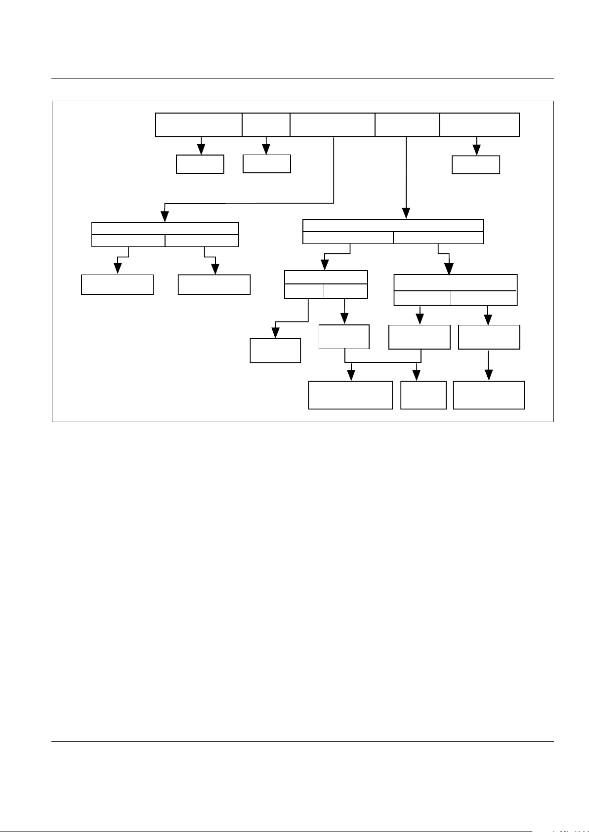
Circuit Requirement Diagram
BILATERAL VOLTAGE
SWITCH
RECTIFIER REVERSE BLOCKING
THYRISTOR
BIDIRECTIONAL
THYRISTOR
BILATERAL
VOLTAGE TRIGGER
SIDAC *
RECTIFIER *
DIAC *
GATE CONTROL
DIAC TRIGGER DIRECT
GATE CURRENT
12-500 µA 10-50 mA
SCR *SCR (Sensitive) *
QUADRANT OPERATION
(See Quadrant Chart on Data Sheet)
I I I I I I I I I I I I I V
GATE CURRENT
10-100 mA
GATE CURRENT
3-20 mA
SENSITIVE TRIAC *
TRIAC *
OPTIONS
INTERNAL EXTERNAL
DIACS *
QUADRAC *
ALTERNISTOR TRIAC *
* For detailed information, see specific data sheet in product catalog.
Page 8
http://www.teccor.com P - 4 ©2002 Teccor Electronics
+1 972-580-7777 Thyristor Product Catalog(972) 580-7777
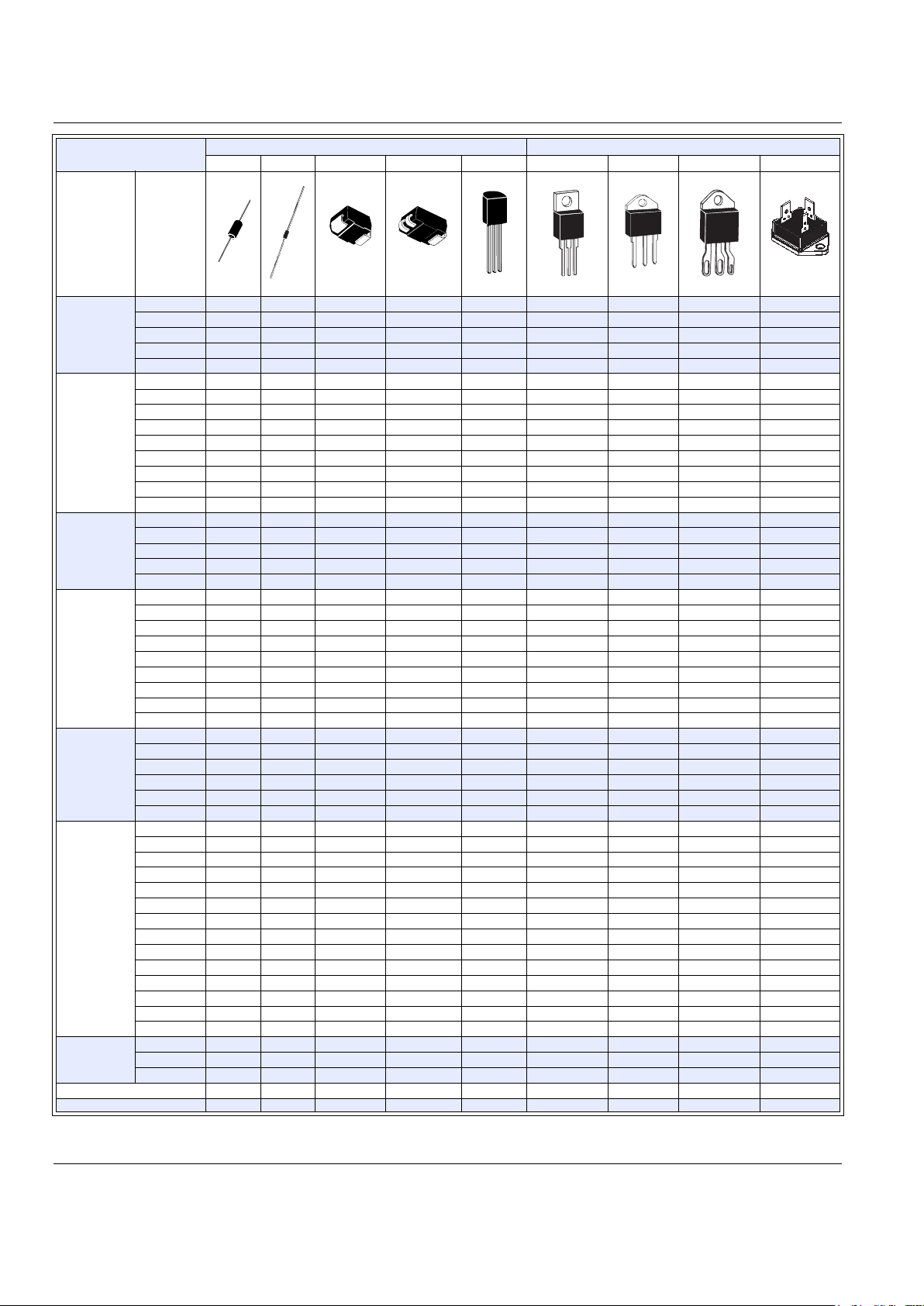
Product Packages
* No center lead on TO-92 Sidacs.
Package Code
Isolated Mounting Tab
GY S C E L K J P
Product
Type
Current
(Amps)
DO-15 DO-35 DO-214 Compak TO-92 * TO-220 TO-218 TO-218X
TO-3
Fastpak
Sensitive
Triac
0.8 ✔ ✔
1 ✔ ✔
4 ✔
6 ✔
8 ✔
Triac
0.8 ✔✔
1 ✔✔
4 ✔
6 ✔
8 ✔
10 ✔
15 ✔
25 ✔
35 ✔
Quadrac
4 ✔
6 ✔
8 ✔
10 ✔
15 ✔
Alternistor
6 ✔
8 ✔
10 ✔
12 ✔
16 ✔
25 ✔✔✔
30 ✔
35
40
✔✔
Sensitive
SCR
0.8 ✔ ✔
1.5 ✔
4
6 ✔
8 ✔
10 ✔
SCR
1 ✔✔
6 ✔
8 ✔
10 ✔
12
15
✔
16
20
✔
25 ✔
35 ✔✔
40
55
65
✔✔
70
Rectifier
15 ✔
20 ✔
25 ✔
Diac
✔✔
Sidac
✔ ✔ ✔ *
Page 9
©2002 Teccor Electronics P - 5 http://www.teccor.com
Thyristor Product Catalog +1 972-580-7777
Product Packages
Non-isolated Mounting Tab
Package Code
FRMWDVN
TO-202 TO-220 TO-218 TO-218X
TO-252
D-Pak
TO-251
V-Pa k
TO-263
D
2
Pak
Current
(Amps)
Product
Typ e
0.8
Sensitive
Triac
1
✔ ✔ ✔ 4
✔ ✔ 6
✔ ✔ 8
0.8
Triac
1
✔ ✔✔ 4
✔✔ ✔ 6
✔✔ ✔ 8
✔✔ ✔ 10
✔ ✔ 15
✔ ✔ 25
35
4
Quadrac
6
8
10
15
✔ ✔✔✔ 6
Alternistor
✔ ✔✔✔ 8
✔ ✔ 10
✔ ✔ 12
✔ ✔ 16
✔ ✔ 25
30
✔ 35
40
✔ 0.8
Sensitive SCR
✔ 1.5
✔ ✔ ✔ ✔ 4
✔ ✔ ✔ ✔ 6
✔ ✔ ✔ ✔ 8
✔ ✔ ✔ ✔ 10
1
SCR
✔ ✔✔ 6
✔✔ ✔✔ 8
✔✔ ✔✔ 10
✔✔✔12
15
✔ ✔ 16
20
✔ ✔ 25
35
✔ ✔ 40
✔✔✔ ✔55
65
✔ 70
15
Rectifier
20
25
Diac
✔
Sidac
Page 10
http://www.teccor.com P - 6 ©2002 Teccor Electronics
+1 972-580-7777 Thyristor Product Catalog(972) 580-7777
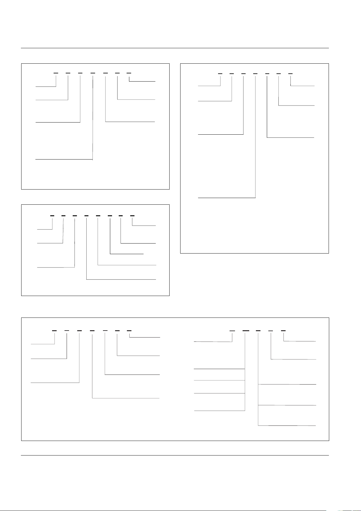
Description of Part Numbers
Sensitive Triac
Quadrac
Sensitive SCR
Triac and Alternistor
L
20
04
F5
12
Device Type
L = Sensitive Triac
Voltage Rating
20 = 200 V
40 = 400 V
60 = 600 V
Current Rating
Package Type
Blank =
Compak
(Surface Mount)
D = TO-252 (Surface Mount)
E = TO-92 (Isolated)
F = TO-202 (Non-islolated)
L = TO-220 (Isolated)
V = TO-251 (Non-islolated)
Gate Variations
3 = 3 mA (Q I, II, III, IV)
5 = 5 mA (Q I, II, III, IV)
6 = 5 mA (Q I, II, III)
6 = 10 mA (Q IV)
8 = 10 mA (Q I, II, III)
8 = 20 mA (Q IV)
Lead Form Dimensions
TO-202
TO-220
TO-92
X
Special Options
V = 4000 V Isolation
(TO-220 Package Only)
X8 = 0.8 A
N = 1 A
01 = 1 A
04 = 4 A
06 = 6 A
08 = 8 A
Q2004 L T 52
Device Type
Q =
Quadrac
Voltage Rating
20 = 200 V
40 = 400 V
60 = 600 V
Current Rating
04 = 4 A
06 = 6 A
08 = 8 A
10 = 10 A
15 = 15 A
Package Type
L = TO-220 (Isolated)
Gate Variation
T = Internal Diac Trigger
Lead Form Dimensions
TO-220
X
Special Options
V = 4000 V Isolation
(TO-220 Package Only)
H
Alternistor
Q
20
04
F3
1
Device Type
Q = Triac or Alternistor
Voltage Rating
20 = 200 V
40 = 400 V
60 = 600 V
80 = 800 V
K0 = 1000 V
Current Rating
X8 = 0.8 A
01 = 1 A
04 = 4 A
06 = 6 A
08 = 8 A
10 = 10 A
12 = 12 A
15 = 15 A
25 = 25 A
30 = 30 A
35 = 35 A
40 = 40 A
Gate Variation
DH3 and VH3 = 10mA (Q I, II, III)
3 = 10 mA (Q I, II, III)
H3 = 20mA (Q I, II, III)
4 = 25 mA (Q I, II, III)
H4 = 35 mA (Q I, II, III) *
5 = 50 mA (Q I, II, III)
H5 = 50 mA (Q I, II, III) *
6 = 80 mA (Q I, II, III) *
7 = 100 mA (Q I, II, III) *
Lead Form Dimensions
TO-202
TO-220
TO-92
TO-218X
TO-218
X
Special Options
V = 4000 V Isolation
(TO-220 Package Only)
Package Type
D = TO-252 (Surface Mount)
E = TO-92 (Isolated)
F = TO-202 (Non-isolated)
J = TO-218X (Isolated)
K = TO-218 (Isolated)
L = TO-220 (Isolated)
N = TO-263 (Surface Mount)
P =
Fastpak
(Isolated)
R = TO-220 (Non-isolated)
V = TO-251 (Non-isolated)
W = TO-218X (Non-isolated)
* NOTE:
Alternistor device; no Quadrant IV operation
S
20
06
FS2
21
Device Type
S = Sensitive SCR
Voltage Rating
20 = 200 V
40 = 400 V
60 = 600 V
Current Rating
X8 = 0.8 A
N = 1 A
06 = 6 A
08 = 8 A
10 = 10 A
Package Type
Blank = Compak (Surface Mount)
D = TO-252 (Surface Mount)
F = TO-202 (Non-islolated)
L = TO-220 (Isolated)
V = TO-251 (Non-islolated)
Gate Variations
S1 = 50 µA
S2 = 200 µA
S3 = 500 µA
Lead Form Dimensions
TO-202
TO-220
X
Special Options
V = 4000 V Isolated
(TO-220 Package Only)
EC
103
D
1
75
Device Type
TCR = TO-92 (Isolated)
EC = TO-92 (Isolated)
T = TO-202 (Non-isolated)
2N = JEDEC (Isolated)
Voltage Rating for TCR
-4 = 200 V
-6 = 400 V
-8 = 600 V
Current Rating for TCR
22 = 1.5 A
Lead Form Dimensions
TO-92
TO-202
Current Rating for EC
103 = 0.8 A
Current Rating for T
106 = 4 A (I
GT
= 200 µA)
107 = 4 A (I
GT
= 500 µA)
Current Rating for 2N
5xxx = 0.8 A
Gate Current (for EC series only)
None = 200 µA
1 = 12 µA
2 = 50 µA
3 = 500 µA
Voltage Rating for EC and T
B = 200 V
D = 400 V
M = 600 V
Voltage Rating for 2N
5064 = 200 V
6565 = 400 V
Page 11
©2002 Teccor Electronics P - 7 http://www.teccor.com
Thyristor Product Catalog +1 972-580-7777
Description of Part Numbers
SCR
Rectifier
Diac
Sidac
S
20
08
F12
Device Type
S = Non-sensitive SCR
Voltage Rating
20 = 200 V
40 = 400 V
60 = 600 V
80 = 800 V
K0 = 1000 V
Current Rating
01 = 1 A
06 = 6 A
08 = 8 A
10 = 10 A
12 = 12 A
15 = 15 A
16 = 16 A
20 = 20 A
25 = 25 A
35 = 35 A
55 = 55 A
65 = 65 A
70 = 70 A
Package Type
D = TO
-
252 (Surface Mount)
E = TO
-
92 (Isolated)
F = TO-202 (Non-isolated)
J = TO-218X (Isolated)
K = TO-218 (Isolated)
L = TO-220 (Isolated)
M = TO-218 (Non-isolated)
N = TO-263 (Surface Mount)
R = TO-220 (Non-isolated)
V = TO-251 (Non-isolated)
W = TO-218X (Non-isolated)
Lead Form Dimensions
TO
-
202
TO
-
220
TO
-
92
TO
-
218X
TO
-
218
X
Special Options
V = 4000 V Isolation
(TO-220 Package Only)
D
20
15
L55
Device Type
D = Rectifier
Voltage Rating
20 = 200 V
40 = 400 V
60 = 600 V
80 = 800 V
K0 = 1000 V
Current Rating
15 = 15 A
20 = 20 A
25 = 25 A
Package Type
L = TO-220 (Isolated)
Lead Form Dimensions
TO-220
V
Special Options
V = 4000 V Isolation
HT
32
91
Device Type
HT = Diac Trigger in DO-35
ST = Diac Trigger in DO-214
Lead Form Dimensions
DO-35
Voltage Rating
32 = 27 V to 37 V
35 = 30 V to 40 V
40 = 35 V to 45 V
32A / 5761 = 28 V to 36 V
32B / 5761A = 30 V to 34 V
34B = 32 V to 36 V
36A / 5762 = 32 V to 40 V
36B = 34 V to 38 V
K
105
0
E70
Device Type
K = Sidac
Voltage Rating
105 = 95 V to 113 V
110 = 104 V to 118 V
120 = 110 V to 125 V
130 = 120 V to 138 V
140 = 130 V to 146 V
150 = 140 V to 170 V
200 = 190 V to 215 V
220 = 205 V to 230 V
240 = 220 V to 250 V
250 = 240 V to 280 V
300 = 270 V to 330 V
Current Rating
0 = 1 A
Package Type
E = TO-92 (Isolated)
F = TO-202 (Non-islolated)
G = DO-15X (Isolated)
S = DO-214 (Surface Mount)
Lead Form Dimensions
TO-202
TO-92
Page 12

http://www.teccor.com P - 8 ©2002 Teccor Electronics
+1 972-580-7777 Thyristor Product Catalog(972) 580-7777
Quality and Reliability
It is Teccor’s policy to ship quality products on time. We accomplish this through Total Quality Management based on the fundamentals of customer focus, continuous improvement, and people
involvement.
In support of this commitment, Teccor applies the following principles:
• Employees shall be respected, involved, informed, and qualified
for their job with appropriate education, training, and experience.
• Customer expectations shall be met or exceeded by consistently
shipping products that meet the agreed specifications, quality
levels, quantities, schedules, and test and reliability parameters.
• Suppliers shall be selected by considering quality, service, delivery, and cost of ownership.
• Design of products and processes will be driven by customer
needs, reliability, and manufacturability.
It is the responsibility of management to incorporate these
principles into policies and systems.
It is the responsibility of those in leadership roles to coach their
people and to reinforce these principles.
It is the responsibility of each individual employee to follow the
spirit of this statement to ensure that we meet the primary policy
— to ship quality products on time.
Quality Assurance
Incoming Material Quality
Teccor “Vendor Analysis” programs provide stringent requirements before components are delivered to Teccor. In addition,
purchased materials are tested rigidly at incoming inspection for
specification compliance prior to acceptance for use.
Process Controls
From silicon slice input through final testing, we use statistical
methods to control all critical processes. Process audits and lot
inspections are performed routinely at all stages of the manufacturing cycle.
Parametric Testing
All devices are 100% computer tested for specific electrical characteristics at critical processing points.
Final Inspection
Each completed manufacturing lot is sampled and tested for
compliance with electrical and mechanical requirements.
Reliability Testing
Random samples are taken from various product families for
ongoing reliability testing.
Finished Goods Inspection
Product assurance inspection is performed immediately prior to
shipping.
Design Assurance
The design and production of Teccor devices is a demanding and
challenging task. Disciplined skills coupled with advanced computer-aided design, production techniques, and test equipment
are essential elements in Teccor's ability to meet your demands
for the very highest levels of quality.
All products must first undergo rigid quality design reviews and
pass extensive environmental life testing. Teccor uses Statistical
Process Control (SPC) with associated control charts throughout
to monitor the manufacturing processes.
Only those products which pass tests designed to assure Teccor's high quality and reliability standards, while economically
satisfying customer requirements, are approved for shipment. All
new products and materials must receive approval of QRA prior
to being released to production.
The combination of reliability testing, process controls, and lot
tracking assures the quality and reliability of Teccor's devices.
Since even the best control systems cannot overcome measurement limitations, Teccor designs and manufactures its own computerized test equipment.
Teccor's Reliability Engineering Group conducts ongoing product
reliability testing to further confirm the design and manufacturing
parameters.
Page 13

©2002 Teccor Electronics P - 9 http://www.teccor.com
Thyristor Product Catalog +1 972-580-7777
Quality and Reliability
Reliability Stress Tests
The following table contains brief descriptions of the reliability tests commonly used in evaluating Teccor product reliability on a periodic basis. These tests are applied across product lines depending on product availability and test equipment capacities. Other tests
may be performed when appropriate.
Flammability Test
For the UL 94V0 flammability test, all expoxies used in Teccor encapsulated devices are recognized by Underwriters Laboratories
Test Ty p e Typical Conditions Test Description Standards
High Temperature
AC Blocking
TA = 100 °C to 150 °C, Bias @
100%
Rated V
DRM
, t = 24 hrs to 1000 hrs
Evaluation of the reliability of
product under bias conditions
and elevated temperature
MIL-STD-750, M-1040
High Temperature
Storage Life
T
A
= 150 °C, t = 250 to 1000 hrs Evaluation of the effects on
devices after long periods of
storage at high temperature
MIL-STD-750, M-1031
Temperature and Humidity
Bias Life
T
A
= 85 °C to 95 °C, rh = 85% to
95%
Bias @ 80% Rated V
DRM
(320 VDC max)
t = 168 to 1008 hrs
Evaluation of the reliability of nonhermetic packaged devices in
humid environments
EIA / JEDEC, JESD22-A101
Temperature Cycle
[Air to Air]
T
A
= -65°C to 150°C,
cycles = 10 to 500
Evaluation of the device’s ability
to withstand the exposure to
extreme temperatures and the
forces of TCE during transitions
between temperatures
MIL-STD-750, M-1051,
EIA / JEDEC, JESD22-A104
Thermal Shock
[Liquid to Liquid]
T
A
= 0 °C to 100 °C, t
txfr
= ≤10 s,
cycled = 10 to 20
Evaluation of the device’s ability
to withstand the sudden changes
in temperature and exposure to
extreme temperatures
MIL-STD-750, M-1056
Autoclave
T
A
= 121 °C, rh = 100%, P = 15 psig,
t = 24 hrs to 168 hrs
Accelerated environmental test to
evaluate the moisture resistance
of plastic packages
EIA / JEDEC, JESD22-A102
Resistance to
Solder Heat
T
A
= 260 °C, t = 10 s Evaluation of the device’s ability
to withstand the temperatures as
seen in wave soldering
operations
MIL-STD-750, M-2031
Solderability
Steam aging = 1 hr to 8 hrs,
T
solder
= 245 °C, Flux = R
Evaluation of the solderability of
device terminals after an
extended period
MIL-STD-750, M-2026,
ANSI-J-STD-002
Page 14

http://www.teccor.com P - 10 ©2002 Teccor Electronics
+1 972-580-7777 Thyristor Product Catalog(972) 580-7777
Standard Terms and Conditions
Supplier shall not be bound by any term proposed by Buyer in the
absence of written agreement to such term signed by an authorized officer of Supplier.
(1) PRICE:
(A) Supplier reserves the right to change product prices at
any time but, whenever practicable, Supplier will give
Buyer at least thirty (30) days written notice before the
effective date of any price change. Unless Supplier has
specifically agreed in writing, signed by an authorized
officer of Supplier, that a quoted price shall not be subject to change for a certain time, all products shipped on
or after the effective date of a price change may be
billed at the new price level.
(B) Whenever Supplier agrees to a modification of Buyer's
order (which modification must be in writing and signed
by an authorized officer of Supplier), Supplier reserves
the right to alter its price, whether or not such price was
quoted as “firm.”
(C) Prices do not include federal, state or local taxes, now or
hereafter enacted, applicable to the goods sold. Taxes
will be added by Supplier to the sales prices whenever
Supplier has legal obligation to collect them and will be
paid by Buyer as invoiced unless Buyer provides Supplier with a proper tax exemption certificate.
(2) PRODUCTION: Supplier may, at its sole discretion and at
any time, withdraw any catalog item from further production
without notice or liability to Buyer.
(3) INTEREST:
(A) All late payments shall bear interest thirty (30) days after
the due date stated on the invoice until paid at the lower
of one and one-half percent per month or the maximum
rate permitted by law. All interest becoming due shall, if
not paid when due, be added to principal and bear interest from the due date. At Supplier's option, any payment
shall be applied first to interest and then to principal.
(B) It is the intention of the parties to comply with the laws of
the jurisdiction governing any agreement between the
parties relating to interest. If any construction of the
agreement between the parties indicates a different
right given to Supplier to demand or receive any sum
greater than that permissible by law as interest, such as
a mistake in calculation or wording, this paragraph shall
override. In any contingency which will cause the interest paid or agreed to be paid to exceed the maximum
rate permitted by law, such excess will be applied to the
reduction of any principal amount due, or if there is no
principal amount due, shall be refunded.
(4) TITLE AND DELIVERY: Title to goods ordered by Buyer and
risk of loss or damage in transit or thereafter shall pass to
Buyer upon Supplier's delivery of the goods at Supplier's
plant or to a common carrier for shipment to Buyer.
(5) CONTINGENCIES: Supplier shall not be responsible for any
failure to perform due to causes reasonably beyond its control. These causes shall include, but not be restricted to, fire,
storm, flood, earthquake, explosion, accident, acts of public
enemy, war rebellion, insurrection, sabotage, epidemic,
quarantine restrictions, labor disputes, labor shortages, labor
slow downs and sit downs, transportation embargoes, failure
or delays in transportation, inability to secure raw materials
or machinery for the manufacture of its devices, acts of God,
acts of the Federal Government or any agency thereof, acts
of any state or local government or agency thereof, and judicial action. Similar causes shall excuse Buyer for failure to
take goods ordered by Buyer, from the time Supplier
receives written notice from Buyer and for as long as the disabling cause continues, other than for goods already in transit or specially fabricated and not readily saleable to other
buyers.
Supplier assumes no responsibility for any tools, dies, and
other equipment furnished Supplier by Buyer.
(6) LIMITED WARRANTY AND EXCLUSIVE REMEDY: Supplier
warrants all catalog products to be free from defects in materials and workmanship under normal and proper use and
application for a period of twelve (12) months from the date
code on the product in question (or if none, from the date of
delivery to Buyer.) With respect to products assembled, prepared, or manufactured to Buyer's specifications, Supplier
warrants only that such products will meet Buyer's specifications upon delivery. As the party responsible for the specifications, Buyer shall be responsible for testing and inspecting
the products for adherence to specifications, and Supplier
shall have no liability in the absence of such testing and
inspection or if the product passes such testing or inspection. THE ABOVE WARRANTY IS THE ONLY WARRANTY
EXTENDED BY SUPPLIER, AND IS IN LIEU OF AND
EXCLUDES ALL OTHER WARRANTIES AND CONDITIONS, EXPRESSED OR IMPLIED (EXCEPT AS PROVIDED HEREIN AS TO TITLE), ON ANY GOODS OR
SERVICES SOLD OR RENDERED BY SUPPLIER, INCLUDING ANY IMPLIED WARRANTIES OF MERCHANTABILITY
AND FITNESS FOR A PARTICULAR PURPOSE. THIS
WARRANTY WILL NOT CREATE WARRANTY COVERAGE
FOR ANY ITEM INTO WHICH ANY PRODUCT SOLD BY
SUPPLIER MAY HAVE BEEN INCORPORATED OR
ADDED.
Page 15

©2002 Teccor Electronics P - 11 http://www.teccor.com
Thyristor Product Catalog +1 972-580-7777
Standard Terms and Conditions
SUPPLIER'S ENTIRE LIABILITY AND BUYER'S EXCLUSIVE REMEDY UNDER THIS WARRANTY SHALL BE, AT
SUPPLIER'S OPTION, EITHER THE REPLACEMENT OF,
REPAIR OF, OR ISSUANCE OF CREDIT TO BUYER'S
ACCOUNT WITH SUPPLIER FOR ANY PRODUCTS
WHICH ARE PROPERLY RETURNED BY BUYER DURING
THE WARRANTY PERIOD. All returns must comply with the
following conditions:
(A) Supplier is to be promptly notified in writing upon discov-
ery of defects by Buyer.
(B) Buyer must obtain a Return Material Authorization
(RMA) number from the Supplier prior to returning product.
(C) The defective product is returned to Supplier, transporta-
tion charges prepaid by Buyer.
(D) Supplier's examination of such product discloses, to its
satisfaction, that such defects have not been caused by
misuse, neglect, improper installation, repair, alteration,
or accident.
(E) The product is returned in the form it was delivered with
any necessary disassembly carried out by Buyer at
Buyer's expense.
IN NO EVENT SHALL SUPPLIER, OR ANYONE ELSE
ASSOCIATED IN THE CREATION OF ANY OF SUPPLIER'S
PRODUCTS OR SERVICES, BE LIABLE TO BUYER FOR
INCIDENTAL OR CONSEQUENTIAL DAMAGES OF ANY
NATURE INCLUDING LOSS OF PROFITS, LOSS OF USE,
BUSINESS INTERUPTION, AND THE LIKE. BUYER
ACKNOWLEDGES THAT THE ABOVE WARRANTIES AND
LIMITATIONS THEREON ARE APPROPRIATE AND REASONABLE IN EFFECTUATING SUPPLIER'S AND BUYER'S
MUTUAL INTENTION TO CONDUCT AN EFFICIENT
TRANSACTION AT PRICES MORE ADVANTAGEOUS TO
BUYER THAN WOULD BE AVAILABLE IN THE PRESENCE
OF OTHER WARRANTIES AND ASSURANCES.
(7) PATENTS: Buyer shall notify Supplier in writing of any claim
that any product or any part of use thereof furnished under
this agreement constitutes an infringement of any U.S.
patent, copyright, trade secret, or other proprietary rights of a
third party. Notice shall be given within a reasonable period
of time which should in most cases be within ten (10) days of
receipt by Buyer of any letter, summons, or complaint pertaining to such a claim. At its option, Supplier may defend at
its expense any action brought against Buyer to the extent
that it is based on such a claim. Should Supplier choose to
defend any such claim, Supplier may fully participate in the
defense, settlement, or appeal of any action based on such
claim.
Should any product become, or in Supplier's opinion be likely
to become, the subject of an action based on any such claim,
Supplier may, at its option, as the Buyer's exclusive remedy,
either procure for the Buyer the right to continue using the
product, replace the product or modify the product to make it
noninfringing. IN NO EVENT SHALL SUPPLIER BE LIABLE
FOR ANY INCIDENTAL OR CONSEQUENTIAL DAMAGES
BASED ON ANY CLAIM OF INFRINGEMENT.
Supplier shall have no liability for any claim based on modifications of a product made by any person or entity other than
Supplier, or based on use of a product in conjunction with
any other item, unless expressly approved by Supplier. Supplier does not warrant goods against claims of infringement
which are assembled, prepared, or manufactured to Buyer's
specifications.
(8) NON-WAIVER OF DEFAULT: Each shipment made under
any order shall be treated as a separate transaction, but in
the event of any default by Buyer, Supplier may decline to
make further shipments without in any way affecting its rights
under such order. If, despite any default by Buyer, Supplier
elects to continue to make shipments, its action shall not
constitute a waiver of that or any default by Buyer or in any
way affect Supplier's legal remedies for any such default. At
any time, Supplier's failure to exercise any right to remedy
available to it shall not constitute a waiver of that right or
remedy.
(9) TERMINATION: If the products to be furnished under this
order are to be used in the performance of a Government
contract or subcontract, and the Government terminates
such contract in whole or part, this order may be canceled to
the extent it was to be used in the canceled portion of said
Government contract and the liability of Buyer for termination
allowances shall be determined by the then applicable regulations of the Government regarding termination of contracts.
Supplier may cancel any unfilled orders unless Buyer shall,
upon written notice, immediately pay for all goods delivered
or shall pay in advance for all goods ordered but not delivered, or both, at Supplier's option.
(10) LAW: The validity, performance and construction of these
terms and conditions and any sale made hereunder shall be
governed by the laws of the state of Texas.
(11) ASSIGNS: This agreement shall not be assignable by
either Supplier or Buyer. However, should either Supplier or
Buyer be sold or transferred in its entirety and as an ongoing
business, or should Supplier or Buyer sell or transfer in its
entirety and as an ongoing concern, any division, department, or subsidiary responsible in whole or in part for the
performance of this Agreement, this Agreement shall be
binding upon and inure to the benefit of those successors
and assigns of Supplier, Buyer, or such division, department,
or subsidiary.
(12) MODIFICATION OF STANDARD TERMS AND CONDI-
TIONS: No attempted or suggested modification of or addition to any of the provisions upon the face or reverse of this
form, whether contained or arising in correspondence and/or
documents passing between Supplier and Buyer, in any
course of dealing between Supplier or Buyer, or in any customary usage prevalent among businesses comparable to
those of Supplier and/or Buyer, shall be binding upon Supplier unless made and agreed to in writing and signed by an
officer of Supplier.
(13) QUANTITIES: Any variation in quantities of electronic com-
ponents, or other goods shipped over or under the quantities
ordered (not to exceed 5%) shall constitute compliance with
Buyer's order and the unit price will continue to apply.
Page 16

Notes
Page 17

©2002 Teccor Electronics http://www.teccor.com
Thyristor Product Catalog +1 972-580-7777
Data Sheets
E0
V-I Characteristics of Thyristor Devices - - - - - - - - - - - - - - - - - - - - - E0-2
Electrical Parameter Terminology - - - - - - - - - - - - - - - - - - - - - - - - - E0-3
Sensitive Triacs- - - - - - - - - - - - - - - - - - - - - - - - - - - - - - - - - - - - - - - E1
Triacs - - - - - - - - - - - - - - - - - - - - - - - - - - - - - - - - - - - - - - - - - - - - - - E2
QUADRACs - - - - - - - - - - - - - - - - - - - - - - - - - - - - - - - - - - - - - - - - - E3
Alternistor Triacs - - - - - - - - - - - - - - - - - - - - - - - - - - - - - - - - - - - - - - E4
Sensitive SCRs - - - - - - - - - - - - - - - - - - - - - - - - - - - - - - - - - - - - - - - E5
SCRs - - - - - - - - - - - - - - - - - - - - - - - - - - - - - - - - - - - - - - - - - - - - - - E6
Rectifiers - - - - - - - - - - - - - - - - - - - - - - - - - - - - - - - - - - - - - - - - - - - E7
Diacs - - - - - - - - - - - - - - - - - - - - - - - - - - - - - - - - - - - - - - - - - - - - - - E8
SIDAC - - - - - - - - - - - - - - - - - - - - - - - - - - - - - - - - - - - - - - - - - - - - - E9
Page 18
http://www.teccor.com E0 - 2 ©2002 Teccor Electronics
+1 972-580-7777 Thyristor Product Catalog
V-I Characteristics of Thyristor Devices
V-I Characteristics of Triac Device
V-I Characteristics of SCR Device
V-I Characteristics of Sidac Device with Negative Resistance
V-I Characteristics of Bilateral Trigger Diac
Breakover
Voltage
Specified Minimum
Off-state
Blocking
Voltage (V
DRM
)
+I
-I
+V
-V
Minimum Holding
Current (I
H
)
Voltage Drop (V
T
) at
Specified Current (i
T
)
Latching Current (I
L
)
Off-state Leakage
Current – (I
DRM
)
at
Specified V
DRM
Reverse
Breakdown
Voltage
Forward
Breakover
Voltage
Specified Minimum
Off - State
Blocking
Voltage (V
DRM
)
+I
-I
+V
-V
Minimum Holding
Current (I
H
)
Voltage Drop (VT) at
Specified Current (i
T
)
Latching Current (IL)
Off - State Leakage
Current - (I
DRM
) at
Specified V
DRM
Specified Minimum
Reverse Blocking
Voltage (V
RRM
)
Reverse Leakage
Current - (I
RRM
) at
Specified V
RRM
-V
+I
V
DRM
+V
V
S
I
S
I
H
R
S
I
DRM
I
BO
V
BO
V
T
I
T
(IS - IBO)
(V
BO
- VS)
R
S
=
-I
+I
-I
10 mA
+V-V
Breakover
Current
I
BO
Breakover
Voltage
V
BO
∆V
Page 19

©2002 Teccor Electronics E0 - 3 http://www.teccor.com
Thyristor Product Catalog +1 972-580-7777
Electrical Parameter Terminology
Thyristor
di/dt (Critical Rate-of-rise of On-state Current) – Maximum
value of the rate-of-rise of on-state current which a thyristor can
withstand without deleterious effect
dv/dt (Critical Rate-of-rise of Off-state Voltage or Static
dv/dt) –
Minimum value of the rate-of-rise of principal voltage
which will cause switching from the off state to the on state
dv/dt(c) Critical Rate-of-rise of Commutation Voltage of a
Triac (Commutating dv/dt) –
Minimum value of the rate-of-rise
of principal voltage which will cause switching from the off state
to the on state immediately following on-state current conduction
in the opposite quadrant
I2t (RMS Surge (Non-repetitive) On-state Fusing Current) –
Measure of let-through energy in terms of current and time for
fusing purposes
I
BO
(Breakover Current) – Principal current at the breakover
point
I
DRM
(Repetitive Peak Off-state Current) – Maximum leakage
current that may occur under the conditions of V
DRM
IGT (Gate Trigger Current) – Minimum gate current required to
switch a thyristor from the off state to the on state
IH (Holding Current) – Minimum principal current required to
maintain the thyristor in the on state
IPP (Peak Pulse Current) – Peak pulse current at a short time
duration and specified waveshape
I
RRM
(Repetitive Peak Reverse Current) – Maximum leakage
current that may occur under the conditions of V
RRM
IS (Switching Current) – Current at V
S
when a sidac switches
from the clamping state to on state
I
T(RMS)
(On-state Current) – Anode cathode principal current
that may be allowed under stated conditions, usually the fullcycle RMS current
I
TSM
(Surge (Non-repetitive) On-state Current) – Peak single
cycle AC current pulse allowed
P
G(AV)
(Average Gate Power Dissipation) – Value of gate
power which may be dissipated between the gate and main terminal 1 (or cathode) average over a full cycle
PGM (Peak Gate Power Dissipation) – Maximum power which
may be dissipated between the gate and main terminal 1 (or
cathode) for a specified time duration
R
θJA
(Thermal Resistance, Junction-to-ambient) – Tempera-
ture difference between the thyristor junction and ambient divided
by the power dissipation causing the temperature difference
under conditions of thermal equilibrium
Note: Ambient is defined as the point where temperature does
not change as a result of the dissipation.
R
θJC
(Thermal Resistance, Junction-to-case) – Temperature
difference between the thyristor junction and the thyristor case
divided by the power dissipation causing the temperature difference under conditions of thermal equilibrium
tgt (Gate-controlled Turn-on Time) – Time interval between
the 10% rise of the gate pulse and the 90% rise of the principal
current pulse during switching of a thyristor from the off state to
the on state
tq (Circuit-commutated Turn-off Time) – Time interval
between the instant when the principal current has decreased to
zero after external switching of the principal voltage circuit and
the instant when the SCR is capable of supporting a specified
principal voltage without turning on
VBO (Breakover Voltage) – Principal voltage at the breakover
point
V
DRM
(Repetitive Peak Off-state Voltage) – Maximum allow-
able instantaneous value of repetitive off-state voltage that may
be applied across a bidirectional thyristor (forward or reverse
direction) or SCR (forward direction only)
V
GT
(Gate Trigger Voltage) – Minimum gate voltage required to
produce the gate trigger current
V
RRM
(Repetitive Peak Reverse Voltage) – Maximum allow-
able instantaneous value of a repetitive reverse voltage that may
be applied across an SCR without causing reverse current avalanche
VS (Switching Voltage) – Voltage point after V
BO
when a sidac
switches from a clamping state to on state
VT (On-state Voltage) – Principal voltage when the thyristor is in
the on state
Diode Rectifiers
I
F(AV)
(Average Forward Current) – Average forward conduc-
tion current
IFM (Maximum (Peak) Reverse Current) – Maximum reverse
leakage current that may occur at rated V
RRM
I
F(RMS)
(RMS Forward Current) – RMS forward conduction cur-
rent
I
FSM
(Maximum (Peak) Forward (Non-repetitive) Surge
Current) –
Maximum (peak) forward single cycle AC surge cur-
rent allowed for specified duration
VFM (Maximum (Peak) Forward Voltage Drop) – Maximum
(peak) forward voltage drop from the anode to cathode at stated
conditions
VR (Reverse Blocking Voltage) – Maximum allowable DC
reverse blocking voltage that may be applied to the rectifier
V
RRM
(Maximum (Peak) Repetitive Reverse Voltage) – Maxi-
mum peak allowable value of a repetitive reverse voltage that
may be applied to the rectifier
Page 20

Notes
Page 21

©2002 Teccor Electronics E1 - 1 http://www.teccor.com
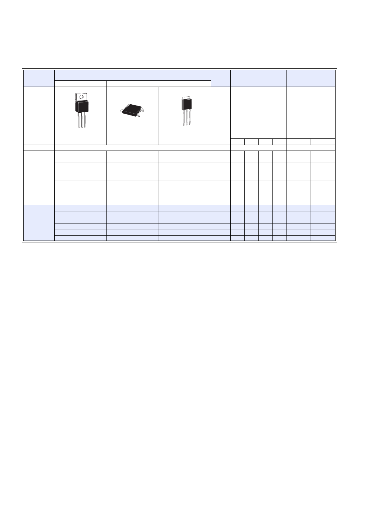
Thyristor Product Catalog +1 972-580-7777
Selected Packages*
U.L. RECOGNIZED
File #E71639
MT2 MT1
G
Sensitive Triacs
(0.8 A to 8 A)
E1
General Description
Teccor's line of sensitive gate triacs includes devices with current
capabilities through 8 A. Voltage ranges are available from 200 V
to 600 V. This line features devices with guaranteed gate control
in Quadrants II and IV as well as control in the commonly used
Quadrants I and III. Four-quadrant control devices require
sensitive gate triacs. They can be controlled by digital circuitry
where positive-only or negative-only pulses must control AC
current in both directions through the device. Note that triacs with
low I
GT
values in Quadrants II and IV will have lower dv/dt
characteristics.
The sensitive gate triac is a bidirectional AC switch and is gate
controlled for either polarity of main terminal voltage. It is used
primarily for AC switching and phase control applications such as
motor speed controls, temperature modulation controls, and
lighting controls.
The epoxy TO-92 and TO-220 configurations feature Teccor's
electrically-isolated construction where the case or mounting tab
is internally isolated from the semiconductor chip and lead
attachments. Non-isolated epoxy TO-202 packages are available
as well as TO-251 and surface mount TO-252 (D-Pak). Tapeand-reel capability and tube packing also are available. See
“Packing Options” section of this catalog.
All Teccor triacs have glass-passivated junctions. This glassing
process prevents migration of contaminants and ensures longterm device reliability with parameter stability.
Variations of devices covered in this data sheet are available for
custom design applications. Consult factory for more information.
Features
• Electrically-isolated packages
• Glass-passivated junctions ensure long device
reliability and parameter stability
• Voltage capability — up to 600 V
• Surge capability — up to 80 A
• Four-quadrant gating guaranteed
Compak Sensitive Gate Triac
• Surface mount package — 0.8 A and 1 A series
• New small profile three-leaded Compak package
• Packaged in embossed carrier tape with 2,500
devices per reel
• Can replace SOT-223
TO-202
TO-92
3-lead
Compak
*TO-220
Isolated
E1
TO-252
D-Pak
TO-251
V-P ak
Page 22
Sensitive Triacs Data Sheets
http://www.teccor.com E1 - 2 ©2002 Teccor Electronics
+1 972-580-7777 Thyristor Product Catalog
See “General Notes” on page E1 - 4 and “Electrical Specification Notes” on page E1 - 5.
I
T(RMS)
Part No.
V
DRM
I
GT
I
DRM
Isolated Non-isolated
(11)
TO-92 Compak TO-220
TO-252
D-Pak TO-202
TO-251
V-Pa k
(1)
Volts
(3) (6) (9)
mAmps
(1) (14)
mAmps
QI QII QIII QIV
T
C
=
25 °C
TC =
110 °C
MAX See “Package Dimensions” section for variations. (12) MIN MAX MAX
0.8 A
L2X8E3 L2X3 200 3 3 3 3 0.01 0.1
L4X8E3 L4X3 400 3 3 3 3 0.01 0.1
L6X8E3 L6X3 600 3 3 3 3 0.01 0.1
L2X8E5 L2X5 200 5 5 5 5 0.01 0.1
L4X8E5 L4X5 400 5 5 5 5 0.01 0.1
L6X8E5 L6X5 600 5 5 5 5 0.01 0.1
L2X8E6 200 5 5 5 10 0.01 0.1
L4X8E6 400 5 5 5 10 0.01 0.1
L6X8E6 600 5 5 5 10 0.01 0.1
L2X8E8 200 10 10 10 20 0.01 0.1
L4X8E8 400 10 10 10 20 0.01 0.1
L6X8E8 600 10 10 10 20 0.01 0.1
1A
L201E3 L2N3 200 33330.01 0.1
L401E3 L4N3 400 33330.01 0.1
L601E3 L6N3 600 33330.01 0.1
L201E5 L2N5 200 55550.01 0.1
L401E5 L4N5 400 55550.01 0.1
L601E5 L6N5 600 55550.01 0.1
L201E6 200 5 5 5 10 0.01 0.1
L401E6 400 5 5 5 10 0.01 0.1
L601E6 600 5 5 5 10 0.01 0.1
L201E8 200 10101020 0.01 0.1
L401E8 400 10101020 0.01 0.1
L601E8 600 10101020 0.01 0.1
4A
L2004L3 L2004D3 L2004F31 L2004V3 200 3 3 3 3 0.01 0.2
L4004L3 L4004D3 L4004F31 L4004V3 400 3 3 3 3 0.01 0.2
L6004L3 L6004D3 L6004F31 L6004V3 600 3 3 3 3 0.01 0.2
L2004L5 L2004D5 L2004F51 L2004V5 200 5 5 5 5 0.01 0.2
L4004L5 L4004D5 L4004F51 L4004V5 400 5 5 5 5 0.01 0.2
L6004L5 L6004D5 L6004F51 L6004V5 600 5 5 5 5 0.01 0.2
L2004L6 L2004D6 L2004F61 L2004V6 200 5 5 5 10 0.01 0.2
L4004L6 L4004D6 L4004F61 L4004V6 400 5 5 5 10 0.01 0.2
L6004L6 L6004D6 L6004F61 L6004V6 600 5 5 5 10 0.01 0.2
L2004L8 L2004D8 L2004F81 L2004V8 200 10 10 10 20 0.01 0.2
L4004L8 L4004D8 L4004F81 L4004V8 400 10 10 10 20 0.01 0.2
L6004L8 L6004D8 L6004F81 L6004V8 600 10 10 10 20 0.01 0.2
MT1
G
MT2
MT2
MT1
G
MT1
MT2
G
MT2
MT2
MT1
G
MT1
G
MT2
MT2
MT2
MT2
G
MT1
Page 23
Data Sheets Sensitive Triacs
©2002 Teccor Electronics E1 - 3 http://www.teccor.com
Thyristor Product Catalog +1 972-580-7777
See “General Notes” on page E1 - 4 and “Electrical Specification Notes” on page E1 - 5.
V
TM
V
GT
I
H
I
GTM
P
GM
P
G(AV)
I
TSM
dv/dt(c) dv/dt
t
gt
I2t di/dt
(1) (4)
Volt s
(2) (5) (15)
Volt s
(1) (7)
mAmps
(13)
Amps
(13)
Watts Watts
(8) (10)
Amps
(1) (10)
Volt s/µSe c
(1)
Vol ts/µSec
(9)
µSec Amps
2
Sec Amps/µSec
T
C
=
25 °C
TC =
25 °C60/50Hz
TC =
100 °C
MAX MAX MAX TYP TYP TYP
1.6 2 5 1 10 0.2 10/8.3 0.5 20 2.8 0.41 20
1.6 2 5 1 10 0.2 10/8.3 0.5 15 2.8 0.41 20
1.6 2 5 1 10 0.2 10/8.3 0.5 10 2.8 0.41 20
1.6 2 10 1 10 0.2 10/8.3 1 20 3 0.41 20
1.6 2 10 1 10 0.2 10/8.3 1 15 3 0.41 20
1.6 2 10 1 10 0.2 10/8.3 1 10 3 0.41 20
1.6 2 10 1 10 0.2 10/8.3 1 30 3 0.41 20
1.6 2 10 1 10 0.2 10/8.3 1 25 3 0.41 20
1.6 2 10 1 10 0.2 10/8.3 1 20 3 0.41 20
1.6 2 15 1 10 0.2 10/8.3 2 35 3.2 0.41 20
1.6 2 15 1 10 0.2 10/8.3 2 30 3.2 0.41 20
1.6 2 15 1 10 0.2 10/8.3 2 25 3.2 0.41 20
1.625110 0.220/16.70.5 202.81.6 20
1.625110 0.220/16.70.5 202.81.6 20
1.625110 0.220/16.70.5 102.81.6 20
1.6 2 10 1 10 0.2 20/16.7 1 20 3 1.6 20
1.6 2 10 1 10 0.2 20/16.7 1 20 3 1.6 20
1.6 2 10 1 10 0.2 20/16.7 1 10 3 1.6 20
1.6 2 10 1 10 0.2 20/16.7 1 30 3 1.6 20
1.6 2 10 1 10 0.2 20/16.7 1 30 3 1.6 20
1.6 2 10 1 10 0.2 20/16.7 1 20 3 1.6 20
1.6 2 15 1 10 0.2 20/16.7 1 35 3.2 1.6 20
1.6 2 15 1 10 0.2 20/16.7 1 35 3.2 1.6 20
1.6 2 15 1 10 0.2 20/16.7 1 25 3.2 1.6 20
1.6 2 5 1.2 15 0.3 40/33 0.5 25 2.8 6.6 50
1.6 2 5 1.2 15 0.3 40/33 0.5 25 2.8 6.6 50
1.6 2 5 1.2 15 0.3 40/33 0.5 15 2.8 6.6 50
1.6 2 10 1.2 15 0.3 40/33 1 25 3 6.6 50
1.6 2 10 1.2 15 0.3 40/33 1 25 3 6.6 50
1.6 2 10 1.2 15 0.3 40/33 1 15 3 6.6 50
1.6 2 10 1.2 15 0.3 40/33 1 30 3 6.6 50
1.6 2 10 1.2 15 0.3 40/33 1 30 3 6.6 50
1.6 2 10 1.2 15 0.3 40/33 1 20 3 6.6 50
1.6 2 15 1.2 15 0.3 40/33 2 35 3.2 6.6 50
1.6 2 15 1.2 15 0.3 40/33 2 35 3.2 6.6 50
1.6 2 15 1.2 15 0.3 40/33 2 25 3.2 6.6 50
Page 24
Sensitive Triacs Data Sheets
http://www.teccor.com E1 - 4 ©2002 Teccor Electronics
+1 972-580-7777 Thyristor Product Catalog
Specified Test Conditions
di/dt — Maximum rate-of-change of on-state current; IGT = 50 mA with
0.1
µs rise time
dv/dt — Critical rate-of-rise of off-state voltage at rated V
DRM
gate open
dv/dt(c) — Critical rate-of-rise of commutation voltage at rated V
DRM
and I
T(RMS)
commutating di/dt = 0.54 rated I
T(RMS)
/ms; gate
unenergized
I
2
t — RMS surge (non-repetitive) on-state current for period of 8.3 ms
for fusing
I
DRM
— Peak off-state current, gate open; V
DRM
= max rated value
I
GT
— DC gate trigger current in specific operating quadrants;
V
D
= 12 V dc; RL = 60 Ω
I
GTM
— Peak gate trigger current
I
H
— Holding current gate open; initial on-state current = 100 mA dc
I
T(RMS)
— RMS on-state current conduction angle of 360°
I
TSM
— Peak one-cycle surge
P
G(AV)
— Average gate power dissipation
P
GM
— Peak gate power dissipation; I
GT
≤ I
GTM
tgt — Gate controlled turn-on time; IGT = 50 mA with 0.1 µs rise time
V
DRM
— Repetitive peak off-state/blocking voltage
V
GT
— DC gate trigger voltage; VD = 12 V dc; RL = 60 Ω
V
TM
— Peak on-state voltage at max rated RMS current
General Notes
• All measurements are made with 60 Hz resistive load and at an
ambient temperature of +25 °C unless otherwise specified.
• Operating temperature range (T
J
) is -65 °C to +110 °C for TO-92
devices and -40 °C to 110 °C for all other devices.
• Storage temperature range (T
S
) is -65 °C to +150 °C for TO-92
devices, -40 °C to +150 °C for TO-202 devices, and -40 °C to
+125 °C for TO-220 devices.
• Lead solder temperature is a maximum of 230 °C for 10 seconds
maximum at a minimum of 1/16” (1.59 mm) from case.
• The case or lead temperature (T
C
or TL) is measured as shown on
dimensional outline drawings. See “Package Dimensions” section
of this catalog.
I
T(RMS)
Part No.
V
DRM
I
GT
I
DRM
Isolated Non-isolated
(11)
TO-220
TO-252
D-Pak
TO-251
V-Pa k
(1)
Volt s
(3) (6)
mAmps
(1) (14)
mAmps
QI QII QIII QIV T
C
= 25 °C TC = 110 °C
MAX See “Package Dimensions” section for variations. (12) MIN MAX MAX
6A
L2006L5 L2006D5 L2006V5 2005555 0.02 0.5
L4006L5 L4006D5 L4006V5 4005555 0.02 0.5
L6006L5 L6006D5 L6006V5 6005555 0.02 0.5
L2006L6 L2006D6 L2006V6 200 5 5 5 10 0.02 0.5
L4006L6 L4006D6 L4006V6 400 5 5 5 10 0.02 0.5
L6006L6 L6006D6 L6006V6 600 5 5 5 10 0.02 0.5
L2006L8 L2006D8 L2006V8 200 10 10 10 20 0.02 0.5
L4006L8 L4006D8 L4006V8 400 10 10 10 20 0.02 0.5
L6006L8 L6006D8 L6006V8 600 10 10 10 20 0.02 0.5
8A
L2008L6 L2008D6 L2008V6 200 5 5 5 10 0.02 0.5
L4008L6 L4008D6 L4008V6 400 5 5 5 10 0.02 0.5
L6008L6 L6008D6 L6008V6 600 5 5 5 10 0.02 0.5
L2008L8 L2008D8 L2008V8 200 10 10 10 20 0.02 0.5
L4008L8 L4008D8 L4008V8 400 10 10 10 20 0.02 0.5
L6008L8 L6008D8 L6008V8 600 10 10 10 20 0.02 0.5
MT1
MT2
G
MT2
MT2
MT1
G
MT2
MT2
G
MT1
Page 25
Data Sheets Sensitive Triacs
©2002 Teccor Electronics E1 - 5 http://www.teccor.com
Thyristor Product Catalog +1 972-580-7777
Electrical Specification Notes
(1) For either polarity of MT2 with reference to MT1 terminal
(2) For either polarity of gate voltage V
GT
with reference to MT1
terminal
(3) See Gate Characteristics and Definition of Quadrants.
(4) See Figure E1.4 for i
T
versus vT.
(5) See Figure E1.6 for V
GT
versus TC.
(6) See Figure E1.7 for I
GT
versus TC.
(7) See Figure E1.5 for I
H
versus TC.
(8) See Figure E1.9 for surge rating and specific duration.
(9) See Figure E1.8 for t
gt
versus IGT.
(10) See Figure E1.2 and Figure E1.3 for maximum allowable case
temperature at maximum rated current.
(11) See Figure E1.1, Figure E1.2, and Figure E1.3 for T
A
or TC versus
I
T(RMS)
.
(12) See package outlines for lead form configurations. When ordering
special lead forming, add type number as suffix to part number.
(13) Pulse width ≤10 µs
(14) T
C
or T
L
= TJ for test conditions in off state
(15) Minimum non-trigger V
GT
at 110 °C is 0.2 V.
Gate Characteristics
Teccor triacs may be turned on between gate and MT1 terminals
in the following ways:
• In-phase signals (with standard AC line) using Quadrants I
and III
• Application of unipolar pulses (gate always positive or negative), using Quadrants II and III with negative gate pulses and
Quadrants I and IV with positive gate pulses
When maximum surge capability is required, pulses should be a
minimum of one magnitude above I
GT
rating with a steep rising
waveform (
≤1 µs rise time).
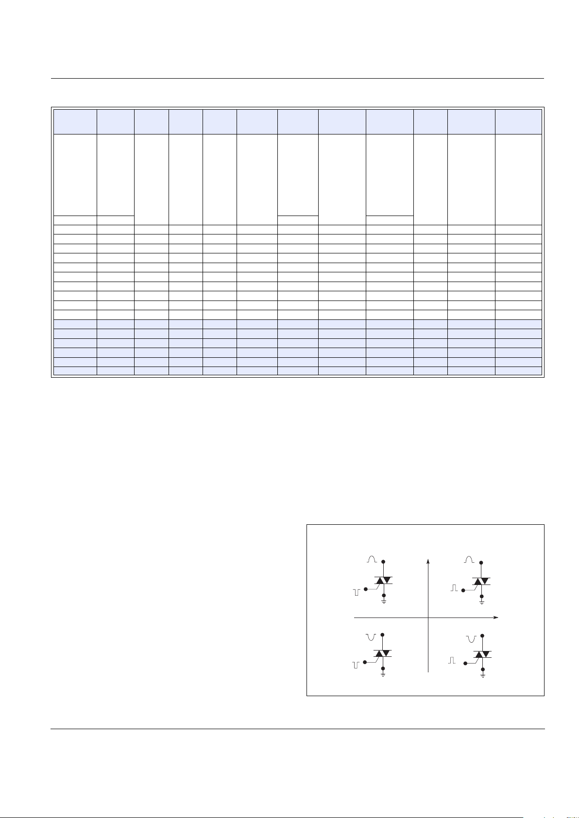
Definition of Quadrants
V
TM
V
GT
I
H
I
GTM
P
GM
P
G(AV)
I
TSM
dv/dt(c) dv/dt
t
gt
I2t di/dt
(1) (4)
Volts
(2) (5) (15)
Volts
(1) (7)
mAmps
(13)
Amps
(13)
Watts Watts
(8) (10)
Amps
(1) (10)
Volts/ µSec
(1)
Volts/ µSec
(9)
µSec Amps
2
Sec Amps/µSec
T
C
= 25 °C TC = 25 °C 60/50 Hz TC = 100 °C
MAX MAX MAX TYP TYP TYP
1.6 2 10 1.6 18 0.4 60/50 1 40 3 15 70
1.6 2 10 1.6 18 0.4 60/50 1 30 3 15 70
1.6 2 10 1.6 18 0.4 60/50 1 20 3 15 70
1.6 2 10 1.6 18 0.4 60/50 2 40 3 15 70
1.6 2 10 1.6 18 0.4 60/50 2 30 3 15 70
1.6 2 10 1.6 18 0.4 60/50 2 20 3 15 70
1.6 2 20 1.6 18 0.4 60/50 2 45 3.2 15 70
1.6 2 20 1.6 18 0.4 60/50 2 40 3.2 15 70
1.6 2 20 1.6 18 0.4 60/50 2 30 3.2 15 70
1.6 2 10 1.6 18 0.4 80/65 2 40 3 26.5 70
1.6 2 10 1.6 18 0.4 80/65 2 30 3 26.5 70
1.6 2 10 1.6 18 0.4 80/65 2 20 3 26.5 70
1.6 2 20 1.6 18 0.4 80/65 2 45 3.2 26.5 70
1.6 2 20 1.6 18 0.4 80/65 2 40 3.2 26.5 70
1.6 2 20 1.6 18 0.4 80/65 2 30 3.2 26.5 70
MT2 POSITIVE
(Positive Half Cycle)
MT2 NEGATIVE
(Negative Half Cycle)
MT1
MT2
+
I
GT
REF
QII
MT1
I
GT
GATE
MT2
REF
MT1
MT2
REF
MT1
MT2
REF
QI
QIV
QIII
ALL POLARITIES ARE REFERENCED TO MT1
(-)
I
GT
GATE
(+)
I
GT
-
I
GT
GATE
(-)
I
GT
GATE
(+)
+
-
Page 26
Sensitive Triacs Data Sheets
http://www.teccor.com E1 - 6 ©2002 Teccor Electronics
+1 972-580-7777 Thyristor Product Catalog
Electrical Isolation
Teccor’s isolated triac packages withstand a minimum high
potential test of 2500 V ac rms from leads to mounting tab over
the device's operating temperature range. The following isolation
table shows standard isolation ratings.
*UL Recognized File #E71639
* Mounted on 1 cm
2
copper foil surface; two-ounce copper foil
Figure E1.1 Maximum Allowable Ambient Temperature versus
On-state Current
Figure E1.2 Maximum Allowable Case Temperature versus
On-state Current (0.8 A and 1 A)
Electrical Isolation
from Leads to Mounting Tab
VACRMS TO-220 *
2500 Standard
Thermal Resistance (Steady State) Junction to Mounting Tab
and Junction to Ambient
R
θJC
[R
θJA
] °C/W (TYP)
Package Code ECFLF2DV
Typ e
TO-92
Plastic Compak
TO-202
Type 1
TO-220
Isolated
TO-202
Type 2
TO-252
D-Pak
TO-251
V-Pa k
0.8 A 60 [135] 60 *
1 A 50 [95] 40 *
4A 3.5 [45] 3.6 [50] 6.0 [70] 3.5 6.0 [70]
6A 3.3 3.2 3.2
8A 2.8 2.7 2.7
20
40
60
80
100
120
RMS On-State Current [I
T(RMS)
] - Amps
Maximum Allowable Ambient Temperature (
T
A
) - ˚C
CURRENT WAVEFORM: Sinusoidal
LOAD: Resistive or Inductive
CONDUCTION ANGLE: 360
˚
FREE AIR RATING – NO HEATSINK
TO-220 and
TYPE 1 and 3 TO-202
TYPE 2 and 4 TO-202
and TO-251
0.8 A TO-92
1 A TO-92
25
0 0.2 0.4 0.6 0.8 1.0 1.2 1.4 1.6 1.8
0 0.2 0.4 0.6 0.8 1.0 1.2 1.4 1.6
50
60
70
80
90
100
110
Maximum Allowable Case Temperature (T
C
) – ˚C
CURRENT WAVEFORM: Sinusoidal
LOAD: Resistive or Inductive
CONDUCTION ANGLE: 360˚
CASE TEMPERATURE: Measured as
shown on Dimensional Drawings
RMS On-State Current [I
T(RMS)
] – Amps
1 A
0.8 A
Page 27
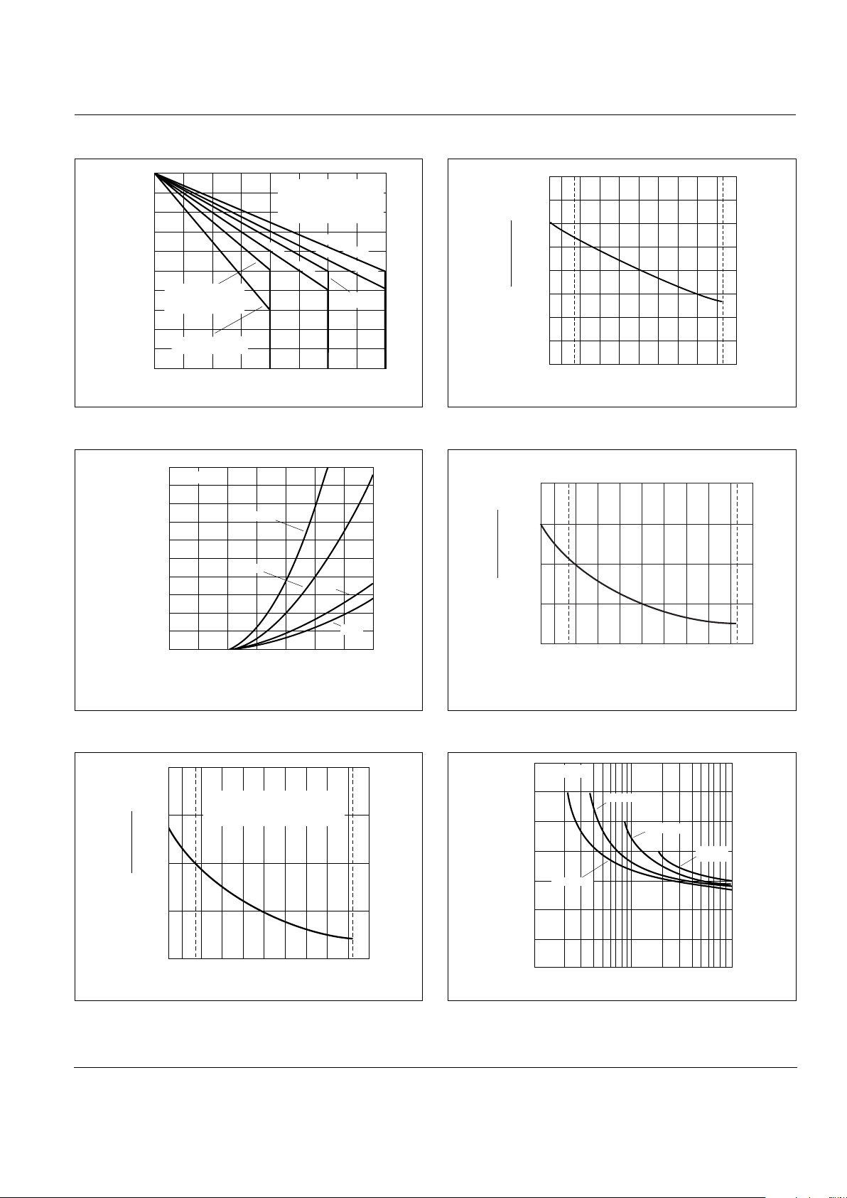
Data Sheets Sensitive Triacs
©2002 Teccor Electronics E1 - 7 http://www.teccor.com
Thyristor Product Catalog +1 972-580-7777
Figure E1.3 Maximum Allowable Case Temperature versus
On-state Current (4 A, 6 A, and 8 A)
Figure E1.4 On-state Current versus On-state Voltage (Typical)
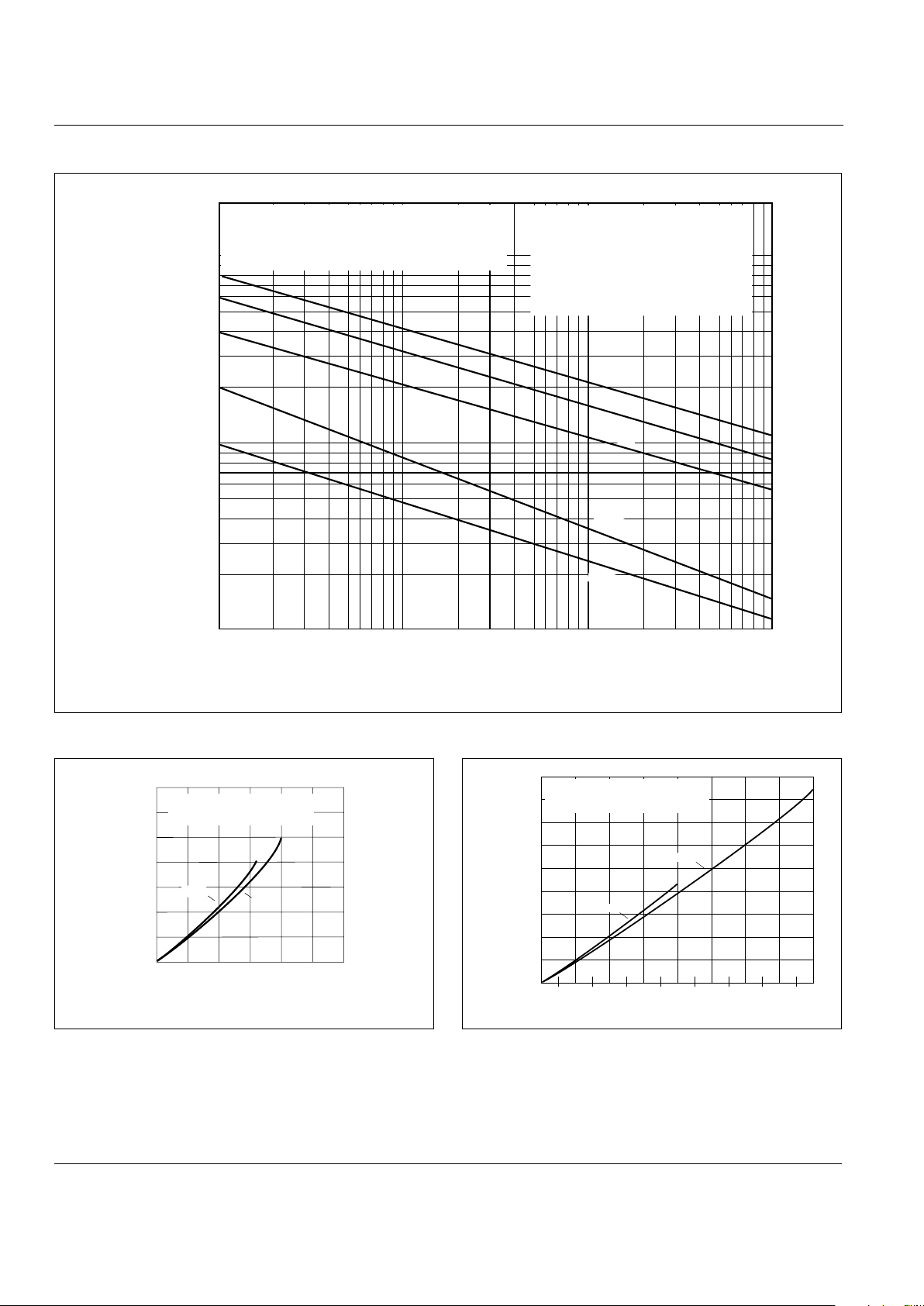
Figure E1.5 Normalized DC Holding Current versus Case Temperature
Figure E1.6 Normalized DC Gate Trigger Voltage for All Quadrants
versus Case Temperature
Figure E1.7 Normalized DC Gate Trigger Current for All Quadrants
versus Case Temperature
Figure E1.8 Turn-on Time versus Gate Trigger Current (Typical)
01 23 4 5 6 7 8
60
65
70
75
80
85
90
95
100
105
110
RMS On-State Current [I
T(RMS)
] - Amps
Maximum Allowable Case Temperature
(
T
C
)
- ˚C
CURRENT WAVEFORM: Sinusoidal
LOAD: Resistive or Inductive
CONDUCTION ANGLE: 360˚
CASE TEMPERATURE: Measured as
shown on Dimensional Drawings
4 A TYPE 1 and 3 TO-202
4 A TO-220 (Isolated)
4 A TO-252
8 A TO-220 (Isolated)
6 A TO-220 (Isolated)
4 A TYPE 2 and 4 TO-202
4 A TO-251
8 A TO-251 and TO-252
6 A TO-251
6 A TO-252
0 0.5 0.8 1.0 1.2 1.4 1.6 1.8
0
2
4
6
8
10
12
14
16
18
20
Positive or Negative Instantaneous
On-state Voltage (v
T
) - Volts
Positive or Negative Instantaneous
On-state Current (i
T
) - Amps
1 A
4 A
6 A and 8 A
TC = 25 ˚C
0.8 A
-40 -15 +25 +65
+110
+125
0
1.0
2.0
3.0
4.0
-65
Case Temperature (
T
C
) - ˚C
INITIAL ON-STATE CURRENT
= 100 mA (DC) 0.8 - 4 A Devices
= 200 mA (DC) 6 - 8 A Devices
Ratio of
I
H
I
H
(T
C
= 25
˚
C)
-65 -40 -15 +65 +110 +125+25
0
.5
1.0
1.5
2.0
Ratio of
V
GT
V
GT
(T
C
= 25 ˚C)
Case Temperature (
T
C
) - ˚C
-65 -40 -15 +65 +110 +125+25
0
1.0
2.0
3.0
4.0
Ratio of
I
GT
I
GT
(T
C
= 25 ˚C)
Case Temperature (TC) - ˚C
123465 8 10 20 30 40 60 80 100
IGT = 5 mA MAX
IGT = 10 mA MAX
IGT = 20 mA
MAX
IGT = 3 mA MAX
0
1.0
2.0
3.0
4.0
5.0
6.0
7.0
DC Gate Trigger Current (IGT) - mA
Turn-On Time (t
gt
) - µSec
TC = 25 ˚C
Page 28
Sensitive Triacs Data Sheets
http://www.teccor.com E1 - 8 ©2002 Teccor Electronics
+1 972-580-7777 Thyristor Product Catalog
Figure E1.9 Peak Surge Current versus Surge Current Duration
Figure E1.10 Power Dissipation (Typical) versus RMS On-state Current
(0.8 A and 1 A)
Figure E1.11 Power Dissipation (Typical) versus RMS On-state Current
(4 A, 6 A, and 8 A)
1 2436810204030 60 100 200 400 600 1000
1
2
3
4
6
10
8
20
30
40
60
100
80
150
200
Surge Current Duration – Full Cycles
Peak Surge (Non-Repetitive)
On-State Current (I
TSM
) – Amps
8 A
6 A
0.8 A
SUPPLY FREQUENCY: 60 Hz Sinusoidal
LOAD: Resistive
RMS On-state Current: [I
T(RMS)
]: Maximum
Rated Value at Specified Case Temperature
NOTES:
1) Gate control may be lost during
and immediately following surge
current interval.
2) Overload may not be repeated until
junction temperature has returned
to steady-state rated value.
1 A
4 A
0 0.25 0.50 0.75 1.0 1.25 1.5
0
0.5
1.0
1.5
RMS On-state Current [I
T(RMS)
] – Amps
Average On-state Power Dissipation
[P
D(AV)
] – Watts
CURRENT WAVEFORM: Sinusoidal
LOAD: Resistive or Inductive
CONDUCTION ANGLE: 360˚
1 A
0.8 A
0 .5 1.0 1.5 2.0 2.5 3.0 3.5 4.0 4.5 5.0 5.5 6.0 6.5 7.0 7.5
0
1.0
2.0
3.0
4.0
5.0
6.0
7.0
8.0
9.0
8.0
6 A and 8 A
4 A
RMS On-state Current [I
T(RMS)
] – Amps
Average On-state Power Dissipation
[P
D(AV)
] – Watts
CURRENT WAVEFORM: Sinusoidal
LOAD: Resistive or Inductive
CONDUCTION ANGLE: 360
˚
Page 29
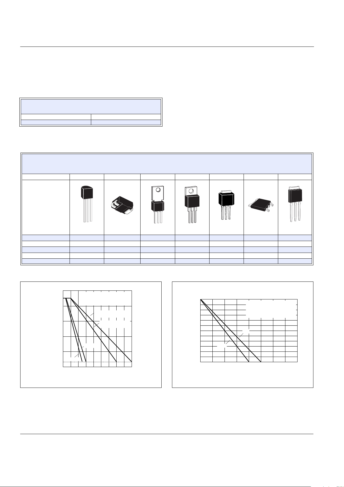
©2002 Teccor Electronics E2 - 1 http://www.teccor.com
Thyristor Product Catalog +1 972-580-7777
Selected Packages*
U.L. RECOGNIZED
File #E71639
Triacs
(0.8 A to 35 A)
E2
General Description
These gated triacs from Teccor Electronics are part of a broad
line of bidirectional semiconductors. The devices range in current
ratings from 0.8 A to 35 A and in voltages from 200 V to 1000 V.
The triac may be gate triggered from a blocking to conduction
state for either polarity of applied voltage and is designed for AC
switching and phase control applications such as speed and temperature modulation controls, lighting controls, and static switching relays. The triggering signal is normally applied between the
gate and MT1.
Isolated packages are offered with internal construction, having
the case or mounting tab electrically isolated from the semiconductor chip. This feature facilitates the use of low-cost assembly
and convenient packaging techniques. Tape-and-reel capability
is available. See “Packing Options” section of this catalog.
All Teccor triacs have glass-passivated junctions to ensure longterm device reliability and parameter stability. Teccor's glass-passivated junctions offer a rugged, reliable barrier against junction
contamination.
Variations of devices covered in this data sheet are available for
custom design applications. Consult factory for more information.
Features
• Electrically-isolated packages
• Glass-passivated junctions
• Voltage capability — up to 1000 V
• Surge capability — up to 200 A
Compak Package
• Surface mount package — 0.8 A and 1 A series
• New small profile three-leaded Compak package
• Packaged in embossed carrier tape with 2,500
devices per reel
• Can replace SOT-223
E2
MT2 MT1
G
TO-202 *TO-220
3-lead
Compak
TO-92
TO-251
V-P ak
TO-263
D
2
Pak
TO-92
TO-252
D-Pak
*TO-3
Fastpak
Page 30
Triacs Data Sheets
http://www.teccor.com E2 - 2 ©2002 Teccor Electronics
+1 972-580-7777 Thyristor Product Catalog
See “General Notes” on page E2 - 4 and “Electrical Specification Notes” on page E2 - 5.
I
T(RMS)
Part Number
V
DRM
I
GT
Isolated Non-isolated
(4)
TO-92 TO-220 Compak TO-202 TO-220
TO-252
D-Pak
TO-251
V-Pa k
TO-263
D
2
Pak
(1)
Volt s
(3) (7) (15)
mAmps
QI QII QIII QIV QIV
MAX See “Package Dimensions” section for variations. (11) MIN MAX TYP
0.8 A
Q2X8E3 Q2X3 200 10 10 10 25
Q4X8E3 Q4X3 400 10 10 10 25
Q6X8E3 Q6X3 600 10 10 10 25
Q2X8E4 Q2X4 200 25 25 25 50
Q4X8E4 Q4X4 400 25 25 25 50
Q6X8E4 Q6X4 600 25 25 25 50
1A
Q201E3 Q2N3 200 101010 25
Q401E3 Q4N3 400 101010 25
Q601E3 Q6N3 600 101010 25
Q201E4 Q2N4 200 252525 50
Q401E4 Q4N4 400 252525 50
Q601E4 Q6N4 600 252525 50
4A
Q2004L3 Q2004F31 Q2004D3 Q2004V3 200 10 10 10 25
Q4004L3 Q4004F31 Q4004D3 Q4004V3 400 10 10 10 25
Q6004L3 Q6004F31 Q6004D3 Q6004V3 600 10 10 10 25
Q2004L4 Q2004F41 Q2004D4 Q2004V4 200 25 25 25 50
Q4004L4 Q4004F41 Q4004D4 Q4004V4 400 25 25 25 50
Q6004L4 Q6004F41 Q6004D4 Q6004V4 600 25 25 25 50
Q8004L4 Q8004D4 Q8004V4 800 25 25 25 50
QK004L4 QK004D4 QK004V4 1000 25 25 25 50
6A
Q2006L4 Q2006F41 Q2006R4 Q2006N4 200 25 25 25 50
Q4006L4 Q4006F41 Q4006R4 Q4006N4 400 25 25 25 50
Q6006L5 Q6006F51 Q6006R5 Q6006N5 600 50 50 50 75
Q8006L5 Q8006R5 Q8006N5 800 50 50 50 75
QK006L5 QK006R5 QK006N5 1000 50 50 50 75
8A
Q2008L4 Q2008F41 Q2008R4 Q2008N4 200 25 25 25 50
Q4008L4 Q4008F41 Q4008R4 Q4008N4 400 25 25 25 50
Q6008L5 Q6008F51 Q6008R5 Q6008N5 600 50 50 50 75
Q8008L5 Q8008R5 Q8008N5 800 50 50 50 75
QK008L5 QK008R5 QK008N5 1000 50 50 50 75
MT1
G
MT2
MT1
MT2
G
G
MT1
MT2
MT2
MT1
G
MT2
MT1
G
MT2
MT2
MT2
MT2
MT1
G
MT2
MT2
G
MT1
MT2
MT2
MT1
G
Page 31

Data Sheets Triacs
©2002 Teccor Electronics E2 - 3 http://www.teccor.com
Thyristor Product Catalog +1 972-580-7777
See “General Notes” on page E2 - 4 and “Electrical Specification Notes” on page E2 - 5.
I
DRM
V
TM
V
GT
I
HIGTM
P
GM
P
G(AV)ITSM
dv/dt(c) dv/dt
t
gt
I2t di/dt
(1) (16)
mAmps
(1) (5)
Volt s
(2) (6)
(15) (18)
(19)
Volt s
(1) (8)
(12)
mAmps
(14)
Amps
(14)
Watts Watts
(9) (13)
Amps
(1) (4) (13)
Vol ts/µ Sec
(1)
Volts/ µSec
(10)
µSec Amp
2
Sec Amps/µSec
T
C
=
25 °C
TC =
100 °C
TC =
125 °C
TC =
25 °C
TC =
25 °C 60/50 Hz
TC=
100 °C
TC=
125 °C
MAX MAX MAX MAX TYP MIN TYP
0.02 0.5 1 1.6 2 15 1 10 0.2 10/8.3 1 40 30 2.5 0.41 20
0.02 0.5 1 1.6 2 15 1 10 0.2 10/8.3 1 35 25 2.5 0.41 20
0.02 0.5 1 1.6 2 15 1 10 0.2 10/8.3 1 25 15 2.5 0.41 20
0.02 0.5 1 1.6 2.5 25 1 10 0.2 10/8.3 1 50 40 3 0.41 20
0.02 0.5 1 1.6 2.5 25 1 10 0.2 10/8.3 1 45 35 3 0.41 20
0.02 0.5 1 1.6 2.5 25 1 10 0.2 10/8.3 1 35 25 3 0.41 20
0.02 0.5 1 1.6 2 15 1 10 0.2 20/16.7 1 40 30 2.5 1.6 30
0.02 0.5 1 1.6 2 15 1 10 0.2 20/16.7 1 40 30 2.5 1.6 30
0.02 0.5 1 1.6 2 15 1 10 0.2 20/16.7 1 30 20 2.5 1.6 30
0.02 0.5 1 1.6 2.5 25 1 10 0.2 20/16.7 1 50 40 3 1.6 30
0.02 0.5 1 1.6 2.5 25 1 10 0.2 20/16.7 1 50 40 3 1.6 30
0.02 0.5 1 1.6 2.5 25 1 10 0.2 20/16.7 1 40 30 3 1.6 30
0.05 0.5 2 1.6 2 20 1.2 15 0.3 55/46 2 50 40 2.5 12.5 50
0.05 0.5 2 1.6 2 20 1.2 15 0.3 55/46 2 50 40 2.5 12.5 50
0.05 0.5 2 1.6 2 20 1.2 15 0.3 55/46 2 40 30 2.5 12.5 50
0.05 0.5 2 1.6 2.5 30 1.2 15 0.3 55/46 2 100 75 3 12.5 50
0.05 0.5 2 1.6 2.5 30 1.2 15 0.3 55/46 2 100 75 3 12.5 50
0.05 0.5 2 1.6 2.5 30 1.2 15 0.3 55/46 2 75 50 3 12.5 50
0.05 0.5 2 1.6 2.5 30 1.2 15 0.3 55/46 2 60 40 3 12.5 50
0.05 3 1.6 2.5 30 1.2 15 0.3 55/46 2 50 3 12.5 50
0.05 0.5 2 1.6 2.5 50 1.6 18 0.5 80/65 4 200 120 3 26.5 70
0.05 0.5 2 1.6 2.5 50 1.6 18 0.5 80/65 4 200 120 3 26.5 70
0.05 0.5 2 1.6 2.5 50 1.6 18 0.5 80/65 4 150 100 3 26.5 70
0.05 0.5 2 1.6 2.5 50 1.6 18 0.5 80/65 4 125 85 3 26.5 70
0.05 3 1.6 2.5 50 1.6 18 0.5 80/65 4 100 3 26.5 70
0.05 0.5 2 1.6 2.5 50 1.8 20 0.5 100/83 4 250 150 3 41 70
0.05 0.5 2 1.6 2.5 50 1.8 20 0.5 100/83 4 250 150 3 41 70
0.05 0.5 2 1.6 2.5 50 1.8 20 0.5 100/83 4 220 125 3 41 70
0.05 0.5 2 1.6 2.5 50 1.8 20 0.5 100/83 4 150 100 3 41 70
0.05 3 1.6 2.5 50 1.8 20 0.5 100/83 4 100 3 41 70
Page 32

Triacs Data Sheets
http://www.teccor.com E2 - 4 ©2002 Teccor Electronics
+1 972-580-7777 Thyristor Product Catalog
Specific Test Conditions
di/dt — Maximum rate-of-change of on-state current; IGT = 200 mA with
≤0.1
µs rise time
dv/dt — Critical rate-of-rise of off-state voltage at rated V
DRM
gate open
dv/dt(c) — Critical rate-of-rise of commutation voltage at rated V
DRM
and I
T(RMS)
commutating di/dt = 0.54 rated I
T(RMS)
/ms; gate
unenergized
I
2
t — RMS surge (non-repetitive) on-state current for period of 8.3 ms
for fusing
I
DRM
— Peak off-state current, gate open; V
DRM
= maximum rated value
I
GT
— DC gate trigger current in specific operating quadrants;
V
D
= 12 V dc
I
GTM
— Peak gate trigger current
I
H
— Holding current (DC); gate open
I
T(RMS)
— RMS on-state current conduction angle of 360°
I
TSM
— Peak one-cycle surge
P
G(AV)
— Average gate power dissipation
P
GM
— Peak gate power dissipation; I
GT
≤ I
GTM
tgt — Gate controlled turn-on time; IGT = 200 mA with 0.1 µs rise time
V
DRM
— Repetitive peak blocking voltage
V
GT
— DC gate trigger voltage; VD = 12 V dc; RL = 60 Ω
V
TM
— Peak on-state voltage at maximum rated RMS current
General Notes
• All measurements are made at 60 Hz with a resistive load at an
ambient temperature of +25 °C unless specified otherwise.
• Operating temperature range (T
J
) is -65 °C to +125 °C for TO-92,
-25 °C to +125 °C for Fastpak, and -40 °C to +125 °C for all other
devices.
• Storage temperature range (T
S
) is -65 °C to +150 °C for TO-92,
-40 °C to +150 °C for TO-202, and -40 °C to +125 °C for all other
devices.
• Lead solder temperature is a maximum of 230 °C for 10 seconds,
maximum; ≥1/16" (1.59 mm) from case.
• The case temperature (T
C
) is measured as shown on the dimensional outline drawings. See “Package Dimensions” section of this
catalog.
I
T(RMS)
Part Number
V
DRM
I
GT
I
DRM
Isolated Non-isolated
(4) (16)
TO-3
Fastpak TO-220 TO -202 TO-220
TO-263
D
2
Pak
(1)
Volt s
(3) (7) (15)
mAmps
(1) (16)
mAmps
QI QII QIII QIV QIV
T
C
=
25 °C
TC =
100 °C
TC =
125 °C
MAX See “Package Dimensions” section for variations. (11) MIN MAX TYP MAX
10 A
Q2010L4 Q2010R4 Q2010N4 200 25 25 25 50 0.05 1
Q4010L4 Q4010R4 Q4010N4 400 25 25 25 50 0.05 1
Q6010L4 Q6010R4 Q6010N4 600 25 25 25 50 0.05 1
Q8010L4 Q8010R4 Q8010N4 800 25 25 25 50 0.1 1
QK010L4 QK010R4 QK010N4 1000 25 25 25 50 0.1 3
Q2010L5 Q2010F51 Q2010R5 Q2010N5 200 50 50 50 75 0.05 0.5 2
Q4010L5 Q4010F51 Q4010R5 Q4010N5 400 50 50 50 75 0.05 0.5 2
Q6010L5 Q6010F51 Q6010R5 Q6010N5 600 50 50 50 75 0.05 0.5 2
Q8010L5 Q8010R5 Q8010N5 800 50 50 50 75 0.1 0.5 2
QK010L5 QK010R5 QK010N5 1000 50 50 50 75 0.1 3
15 A
Q2015L5 Q2015R5 Q2015N5 200 50 50 50 0.05 0.5 2
Q4015L5 Q4015R5 Q4015N5 400 50 50 50 0.05 0.5 2
Q6015L5 Q6015R5 Q6015N5 600 50 50 50 0.05 0.5 2
Q8015L5 Q8015R5 Q8015N5 800 50 50 50 0.1 1 3
QK015L5 QK015R5 QK015N5 1000 50 50 50 0.1 3
25 A
Q2025R5 Q2025N5 200 50 50 50 0.1 1 3
Q4025R5 Q4025N5 400 50 50 50 0.1 1 3
Q6025R5 Q6025N5 600 50 50 50 0.1 1 3
Q8025R5 Q8025N5 800 50 50 50 0.1 1 3
QK025R5 QK025N5 1000 50 50 50 0.1 3
Q6025P5 600 505050 1200.1 5
Q8025P5 800 505050 1200.1 5
35 A
Q6035P5 600 50 50 50 120 0.1 5
Q8035P5 800 50 50 50 120 0.1 5
MT1
MT2
Gate
MT1
MT2
T
MT2
MT1
G
MT2
MT1
G
MT2
MT2
MT2
MT2
MT1
G
Page 33

Data Sheets Triacs
©2002 Teccor Electronics E2 - 5 http://www.teccor.com
Thyristor Product Catalog +1 972-580-7777
Electrical Specification Notes
(1) For either polarity of MT2 with reference to MT1 terminal
(2) For either polarity of gate voltage (V
GT
) with reference to MT1
terminal
(3) See Gate Characteristics and Definition of Quadrants.
(4) See Figure E2.1 through Figure E2.7 for current rating at specific
operating temperature.
(5) See Figure E2.8 through Figure E2.10 for i
T
versus v
T
.
(6) See Figure E2.12 for VGT versus TC.
(7) See Figure E2.11 for I
GT
versus TC.
(8) See Figure E2.14 for I
H
versus TC.
(9) See Figure E2.13 for surge rating with specific durations.
(10) See Figure E2.15 for t
gt
versus IGT.
(11) See package outlines for lead form configurations. When ordering
special lead forming, add type number as suffix to part number.
(12) Initial on-state current = 200 mA dc for 0.8 A to10 A devices,
400 mA dc for 15 A to 35 A devices
(13) See Figure E2.1 through Figure E2.6 for maximum allowable case
temperature at maximum rated current.
(14) Pulse width ≤10
µs; IGT ≤ I
GTM
(15) RL = 60 Ω for 0.8 A to10 A triacs; RL = 30 Ω for 15 A to 35 A triacs
(16) T
C
= TJ for test conditions in off state
(17) I
GT
= 300 mA for 25 A and 35 A devices
(18) Quadrants I, II, III only
(19) Minimum non-trigger V
GT
at 125 °C is 0.2 V for all except 50 mA
MAX QIV devices which are 0.2 V at 110 °C.
Gate Characteristics
Teccor triacs may be turned on between gate and MT1 terminals
in the following ways:
• In-phase signals (with standard AC line) using Quadrants I
and III
• Application of unipolar pulses (gate always positive or negative), using Quadrants II and III with negative gate pulses and
Quadrants I and IV with positive gate pulses
However, due to higher gate requirements for Quadrant IV, it
is recommended that only negative pulses be applied. If positive pulses are required, see “Sensitive Triacs” section of
this catalog or contact the factory. Also, see
Figure AN1002.8, “Amplified Gate” Thyristor Circuit.
V
TM
V
GT
I
H
I
GTM
P
GM
P
G(AV)
I
TSM
dv/dt(c) dv/dt
t
gt
I2t di/dt
(1) (5)
Vol ts
(2) (6) (15)
(18) (19)
Vol ts
(1) (8) (12)
mAmps
(14)
Amps
(14)
Watts Watts
(9) (13)
Amps
(1) (4) (13)
Volt s/µSe c
(1)
Volt s/µSec
(10) (17)
µSec Amps
2
Sec Amps/µSec
T
C
= 25 °C TC = 25 °C 60/50 Hz
T
C
=
100 °C
TC =
125 °C
MAX MAX MAX TYP MIN TYP
1.6 2.5 35 1.8 20 0.5 120/100 2 150 3 60 70
1.6 2.5 35 1.8 20 0.5 120/100 2 150 3 60 70
1.6 2.5 35 1.8 20 0.5 120/100 2 100 3 60 70
1.6 2.5 35 1.8 20 0.5 120/100 2 75 3 60 70
1.6 2.5 35 1.8 20 0.5 120/100 2 50 3 60 70
1.6 2.5 50 1.8 20 0.5 120/100 4 350 225 3 60 70
1.6 2.5 50 1.8 20 0.5 120/100 4 350 225 3 60 70
1.6 2.5 50 1.8 20 0.5 120/100 4 300 200 3 60 70
1.6 2.5 50 1.8 20 0.5 120/100 4 250 175 3 60 70
1.6 2.5 50 1.8 20 0.5 120/100 4 150 3 60 70
1.6 2.5 70 2 20 0.5 200/167 4 400 275 4 166 100
1.6 2.5 70 2 20 0.5 200/167 4 400 275 4 166 100
1.6 2.5 70 2 20 0.5 200/167 4 350 225 4 166 100
1.6 2.5 70 2 20 0.5 200/167 4 300 200 4 166 100
1.6 2.5 70 2 20 0.5 200/167 4 200 4 166 100
1.8 2.5 100 2 20 0.5 200/167 5 400 275 4 166 100
1.8 2.5 100 2 20 0.5 200/167 5 400 275 4 166 100
1.8 2.5 100 2 20 0.5 200/167 5 350 225 4 166 100
1.8 2.5 100 2 20 0.5 200/167 5 300 200 4 166 100
1.8 2.5 100 2 20 0.5 200/167 5 200 4 166 100
1.4 2.75 50 2 20 0.5 250/220 5 550 475 3 260 100
1.4 2.75 50 2 20 0.5 250/220 5 450 400 3 260 100
1.5 2.75 50 2 20 0.5 350/300 5 550 475 3 508 100
1.5 2.75 50 2 20 0.5 350/300 5 450 400 3 508 100
Page 34

Triacs Data Sheets
http://www.teccor.com E2 - 6 ©2002 Teccor Electronics
+1 972-580-7777 Thyristor Product Catalog
In all cases, if maximum surge capability is required, pulses
should be a minimum of one magnitude above I
GT
rating with a
steep rising waveform (≤1 µs rise time).
Definition of Quadrants
Electrical Isolation
Teccor’s isolated triac packages will withstand a minimum high
potential test of 2500 V ac rms from leads to mounting tab or
base, over the operating temperature range of the device. The
following isolation table shows standard and optional isolation
ratings.
* UL Recognized File E71639
** For 4000 V isolation, use V suffix in part number.
* Mounted on 1 cm
2
copper foil surface; two-ounce copper foil
MT2 POSITIVE
(Positive Half Cycle)
MT2 NEGATIVE
(Negative Half Cycle)
MT1
MT2
+
I
GT
REF
QII
MT1
I
GT
GATE
MT2
REF
MT1
MT2
REF
MT1
MT2
REF
QI
QIV
QIII
ALL POLARITIES ARE REFERENCED TO MT1
(-)
I
GT
GATE
(+)
I
GT
-
I
GT
GATE
(-)
I
GT
GATE
(+)
+
-
Electrical Isolation
from Leads to Mounting Tab *
VACRMS
TO-220
Isolated
Fastpak
Isolated
2500 Standard Standard
4000 Optional ** N/A
Thermal Resistance (Steady State)
R
θ JC
[R
θ JA
] (TYP.) °C/W
Package Code PECFF2LR D V N
Typ e
TO-3
Fastpak TO-92
Compak
TO-202
Type 1
TO-202
Type 2
TO-220
Isolated
TO-220
Non-isolated
TO-252
D-Pak
TO-251
V-Pa k
TO-263
D
2
Pak
0.8 A 60 [135] 60 *
1 A 50 [95] 40 *
4A 3.5 [45] 6 [70] 3.6 [50] 3.5 6.0 [70]
6 A 3.8 3.3 1.8 [45] 1.8
8A 3.3 2.8 1.5 1.5
10 A 3.5 2.6 1.3 1.3
15 A 2.1 1.1 1.1
25 A 1.6 0.89 0.89
35 A 1.5
Page 35

Data Sheets Triacs
©2002 Teccor Electronics E2 - 7 http://www.teccor.com
Thyristor Product Catalog +1 972-580-7777
Figure E2.1 Maximum Allowable Case Temperature versus On-state
Current (0.8 A and 1 A)
Figure E2.2 Maximum Allowable Case Temperature versus On-state
Current (4 A and 6 A)
Figure E2.3 Maximum Allowable Case Temperature versus
On-state Current (8 A and 10 A)
Figure E2.4 Maximum Allowable Case Temperature versus
On-state Current (10 A)
Figure E2.5 Maximum Allowable Case Temperature versus
On-state Current (15 A)
Figure E2.6 Maximum Allowable Case Temperature versus
On-state Current (25 A and 35 A)
0 0.2 0.4 0.6 0.8 1.0 1.2 1.4
0
60
70
80
90
100
110
120
130
RMS On-state Current [l
T(RMS)
] – AMPS
Maximum Allowable Case Temperature (T
C
) –
˚
C
CURRENT WAVEFORM: Sinusoidal
LOAD: Resistive or Inductive
CONDUCTION ANGLE: 360
˚
CASE TEMPERATURE: Measured
as shown on Dimensional Drawing
1 A
0.8 A
01234567
0
60
70
80
90
100
110
120
130
RMS On-state Current [l
T(RMS)
] – Amps
Maximum Allowable Case Temperature (T
C
) –
˚
C
6 A TO-220 (Isolated)
6 A TO-202
6 A TO-220 (Non-isolated)
6 A D
2
Pak
4 A TO-220 (Isolated)
4 A TO-202 (Type 1 and 3)
4 A TO-252
CURRENT WAVEFORM: Sinusoidal
LOAD: Resistive or Inductive
CONDUCTION ANGLE: 360
˚
CASE TEMPERATURE: Measured as
shown on Dimensional Drawing
4 A TO-202 (TYPE 2 and 4)
4 A TO-251
02468101214
0
60
70
80
90
100
110
120
130
RMS On-state Current [l
T(RMS)
] – AMPS
Maximum Allowable Case Temperature (T
C
) – ˚C
10 A TO-220 (Isolated)
8 A TO-220 (Non-isolated)
8 A D
2
Pak
8 A TO-202
8 A TO-220 (Isolated)
CURRENT WAVEFORM: Sinusoidal
LOAD: Resistive or Inductive
CONDUCTION ANGLE: 360
˚
CASE TEMPERATURE: Measured as
shown on Dimensional Drawing
02468101214
0
60
70
80
90
100
110
120
130
RMS On-state Current [l
T(RMS)
] – Amps
Maximum Allowable Case Temperature (T
C
) – ˚C
CURRENT WAVEFORM: Sinusoidal
LOAD: Resistive or Inductive
CONDUCTION ANGLE: 360
˚
CASE TEMPERATURE: Measured as
shown on Dimensional Drawing
10 A TO-202
10 A TO-220 (Non-isolated)
10 A D
2
Pak
051015
0
60
70
80
90
100
110
120
130
RMS On-state Current [l
T(RMS)
] – AMPS
Maximum Allowable Case Temperature (T
C
) – ˚C
CURRENT WAVEFORM: Sinusoidal
LOAD: Resistive or Inductive
CONDUCTION ANGLE: 360
˚
CASE TEMPERATURE: Measured as
shown on Dimensional Drawing
15 A TO-220 (Non-isolated)
15 A D
2
Pak
15 A TO-220 (Isolated)
0 1020304050
50
60
70
80
90
100
110
120
130
RMS On-state Current [l
T(RMS)
] – Amps
Maximum Allowable Case Temperature (T
C
) – ˚C
CURRENT WAVEFORM: Sinusoidal
LOAD: Resistive or Inductive
CONDUCTION ANGLE: 360˚
CASE TEMPERATURE: Measured as
shown on Dimensional Drawing
25 A TO-220 (Non-isolated)
25 A D
2
Pak
25 A TO-3 Fastpak
35 A TO-3 Fastpak
Page 36

Triacs Data Sheets
http://www.teccor.com E2 - 8 ©2002 Teccor Electronics
+1 972-580-7777 Thyristor Product Catalog
Figure E2.7 Maximum Allowable Ambient Temperature versus
On-state Current
Figure E2.8 On-state Current versus On-state Voltage (Typical)
(0.8 A and 1 A)
Figure E2.9 On-state Current versus On-state Voltage (Typical)
(4 A, 6 A, 8 A, and 10 A)
Figure E2.10 On-state Current versus On-state Voltage (Typical)
(15 A and 25 A)
Figure E2.11 Normalized DC Gate Trigger Current for All Quadrants
versus Case Temperature
Figure E2.12 Normalized DC Gate Trigger Voltage for All Quadrants
versus Case Temperature
120
100
80
60
40
25
20
0 0.2 0.4 0.6 0.8 1.0 1.2 1.4 1.6 1.8 2.0
TO-220 Devices and
TO-202 (Type 1 and 3)
RMS On-state Current [I
T (RMS)
] — Amps
Maximum Allowable Ambient Temperature (T
A
) — ˚C
1 A TO-92
0.8 A TO-92
CURRENT WAVEFORM: Sinusoidal
LOAD: Resistive or Inductive
CONDUCTION ANGLE: 360
˚
FREE AIR RATING – NO HEATSINK
TO-202 (TYPE 2 and 4)
TO-251
0 0.6 0.8 1.0 1.2 1.4 1.6 1.8
0
1
2
3
4
5
6
7
8
9
10
Positive or Negative Instantaneous On-state Voltage (vT) – Volts
Positive or Negative Instantaneous On-state Current (i
T
) – Amps
T
C
= 25 ˚C
1 A
0.8 A
0 0.6 0.8 1.0 1.2 1.4 1.6 1.8
0
2
4
6
8
10
12
14
16
18
20
Positive or Negative Instantaneous On-state Voltage (vT) – Volts
Positive or Negative Instantaneous
On-state Current (i
T
) – Amps
TC = 25 ˚C
6-10 A
4A
0 0.6 0.8 1.0 1.2 1.4 1.6 1.8
0
10
20
30
40
50
60
70
80
90
Positive or Negative Instantaneous On-state Voltage (vT) – Volts
Positive or Negative Instantaneous
On-state Current (i
T
) – Amps
TC = 25 ˚C
15 A and 25 A
15 A and 25 A Fastpak
-65 -40 -15 +25 +65 +125
1.0
2.0
3.0
4.0
Case Temperature (TC) – ˚C
Ratio of
I
GT
I
GT
(T
C
= 25 ˚C)
-65 -15-40 +25 +65 +125
0
.5
1.0
1.5
2.0
Case Temperature (TC) – ˚C
Ratio of
V
GT
V
GT
(T
C
= 25 ˚C)
Page 37

Data Sheets Triacs
©2002 Teccor Electronics E2 - 9 http://www.teccor.com
Thyristor Product Catalog +1 972-580-7777
Figure E2.13 Peak Surge Current versus Surge Current Duration
Figure E2.14 Normalized DC Holding Current versus Case Temperature Figure E2.15 Turn-on Time versus Gate Trigger Current (Typical)
SUPPLY FREQUENCY: 60 Hz Sinusoidal
LOAD: Resistive
RMS ON-STATE CURRENT [l
T(RMS)
]: Maximum
Rated Value at Specified Case Temperature
NOTES:
1) Gate control may be lost during and
immediately following surge current interval.
2) Overload may not be repeated until
junction temperature has returned to
steady-state rated value.
25 A TO
-220
15 A
10 A
8 A
4 A
1 A
6 A
1
10
20
30
40
50
60
80
100
120
300
400
1000
1 10 100 1000
Surge Current Duration – Full Cycles
Peak Surge (Non-repetitive) On-state Current (l
TSM
) – Amps
200
0.8 A
25 A Fastpak
35 A Fastpak
-65 -40 -15 +25 +65 +125
1.0
2.0
3.0
4.0
Case Temperature (TC) – ˚C
Ratio of
I
H
I
H
(T
C
= 25 ˚C)
INITIAL ON-STATE CURRENT
= 200 mA DC 0.8 A - 10 A Devices
= 400 mA DC 15 A - 25 A Devices
0
0 25 50 75 100 125 150 175 200 225 250 275 300
1
2
3
4
5
6
7
8
Typical Turn-on Time (t
gt
) – µSec
DC Gate Trigger Current (lGT) – mA
Devices with
l
GT
= 10 mA
Devices with
l
GT
= 25 mA
Devices with
l
GT
= 50 mA
TC = 25 ˚C
Page 38

Triacs Data Sheets
http://www.teccor.com E2 - 10 ©2002 Teccor Electronics
+1 972-580-7777 Thyristor Product Catalog
Figure E2.16 Power Dissipation (Typical) versus On-state Current
(0.8 A and 1 A)
Figure E2.17 Power Dissipation (Typical) versus On-state Current
(6 A to 10 A and 15 A)
Figure E2.18 Power Dissipation (Typical) versus On-state Current
(25 A to 35 A)
Figure E2.19 Power Dissipation (Typical) versus RMS On-state Current
(4 A)
RMS On-state Current [I
T(RMS)
] – Amps
Average On-state Power Dissipation
[P
D(AV)
] – Watts
0 0.25 0.50 0.75 1.0 1.25
0
0.5
1.0
1.5
CURRENT WAVEFORM: Sinusoidal
LOAD: Resistive or Inductive
CONDUCTION ANGLE: 360˚
1 A
0.8 A
012345678910111213141516
0
2
4
6
8
10
12
14
16
18
RMS On-state Current [l
T(RMS)
] – Amps
Average On-state Power Dissipation [P
D(AV)
] – Watts
6-10 A
15 A
CURRENT WAVEFORM: Sinusoidal
LOAD: Resistive or Inductive
CONDUCTION ANGLE: 360˚
0 8 16 24 32 40
0
5
10
15
20
25
30
35
40
45
RMS On-state Current [l
T(RMS)
] – Amps
Average On-state Power Dissipation [P
D(AV)
] – Watts
CURRENT WAVEFORM: Sinusoidal
LOAD: Resistive or Inductive
CONDUCTION ANGLE: 360˚
25 A
25 A - 35 A Fastpaks
RMS On-state Current [I
T(RMS)
] – Amps
Average On-state Power Dissipation
[P
D(AV)
] – Watts
0 1.0 2.0 3.0 4.0
0
1.0
2.0
3.0
CURRENT WAVEFORM: Sinusoidal
LOAD: Resistive or Inductive
CONDUCTION ANGLE: 360˚
4 A
4.0
Page 39

©2002 Teccor Electronics E3 - 1 http://www.teccor.com
Thyristor Product Catalog +1 972-580-7777
U.L. RECOGNIZED
File #E71639
Quadrac
Internally Triggered Triacs (4 A to 15 A)
E3
General Description
Te cc o r’ s Quadrac devices are triacs that include a diac trigger
mounted inside the same package. This device, developed by
Teccor, saves the user the expense and assembly time of buying
a discrete diac and assembling in conjunction with a gated triac.
Also, the alternistor Quadrac device (QxxxxLTH) eliminates the
need for a snubber network.
The Quadrac device is a bidirectional AC switch and is gate controlled
for either polarity of main terminal voltage. Its primary purpose is for AC switching and phase control applications such as
speed controls, temperature modulation controls, and lighting
controls where noise immunity is required.
Triac current capacities range from 4 A to 15 A with voltage
ranges from 200 V to 600 V. Quadrac devices are available in the
TO-220 package.
The TO-220 package is electrically isolated to 2500 V rms from
the leads to mounting surface. 4000 V rms is available on special
order. This means that no external isolation is required, thus
eliminating the need for separate insulators and insulator-mounting steps and saving dollars over “hot tab” devices.
All Teccor triac and diac chips have glass-passivated junctions to
ensure long-term device reliability and parameter stability.
Variations of devices in this data sheet are available for custom
design applications. Consult the factory for more information.
Features
• Glass-passivated junctions
• Electrically-isolated package
• Internal trigger diac
• High surge capability — up to 200 A
• High voltage capability — 200 V to 600 V
TO-220
Isolated
MT2 MT1
T
E3
Page 40

Quadrac Data Sheets
http://www.teccor.com E3 - 2 ©2002 Teccor Electronics
+1 972-580-7777 Thyristor Product Catalog
Specific Test Conditions
[∆V±] — Dynamic breakback voltage (forward and reverse)
∆V
BO
— Breakover voltage symmetry
C
T
— Trigger firing capacitance
di/dt — Maximum rate-of-change of on-state current
dv/dt — Critical rate-of-rise of off-state voltage at rated V
DRM
gate open
dv/dt(c) — Critical rate-of-rise of commutation voltage at rated V
DRM
and I
T(RMS)
commutating di/dt = 0.54 rated I
T(RMS)
/ms; gate
unenergized
I
2
t — RMS surge (non-repetitive) on-state current for period of 8.3 ms
for fusing
I
BO
— Peak breakover current
I
DRM
— Peak off-state current gate open; V
DRM
= maximum rated value
I
GTM
— Peak gate trigger current (10 µs Max)
I
H
— Holding current; gate open
I
T(RMS)
— RMS on-state current, conduction angle of 360°
I
TSM
— Peak one-cycle surge
t
gt
— Gate controlled turn-on time
V
BO
— Breakover voltage (forward and reverse)
V
DRM
— Repetitive peak blocking voltage
V
TM
— Peak on-state voltage at maximum rated RMS current
General Notes
• All measurements are made at 60 Hz with resistive load at an ambi-
ent temperature of +25 °C unless otherwise specified.
• Operating temperature range (T
J
) is -40 °C to +125 °C.
• Storage temperature range (T
S
) is -40 °C to +125 °C.
• Lead solder temperature is a maximum of +230 °C for 10 seconds
maximum; ≥1/16" (1.59 mm) from case.
• The case temperature (T
C
) is measured as shown on dimensional
outline drawings. See “Package Dimensions” section of this
catalog.
Electrical Specification Notes
(1) For either polarity of MT2 with reference to MT1
(2) See Figure E3.1 for I
H
versus TC.
(3) See Figure E3.4 and Figure E3.5 for i
T
versus vT.
(4) See Figure E3.9 for surge ratings with specific durations.
I
T(RMS)
Part No.
V
DRM
I
DRM
V
TM
Trigger Diac Specifications (T–MT1)
Isolated ∆V
BO
V
BO
[∆V± ]IBOC
T
(5)
TO-220
(1)
Vol ts
(1) (10)
mAmps
(1) (3)
Volts
(7)
Volt s
(6)
Vol ts
(6)
Volts µAmps
(11)
µFarads
T
C
=
25 °C
TC =
100 °C
TC =
125 °C T
C
= 25 °C
See “Package Dimensions” section
for variations. (12) MIN MAX MAX MAX MIN MAX MIN MAX MAX
4A
Q2004LT 200 0.05 0.5 2 1.6 3 33 43 5 25 0.1
Q4004LT 400 0.05 0.5 2 1.6 3 33 43 5 25 0.1
Q6004LT 600 0.05 0.5 2 1.6 3 33 43 5 25 0.1
6A
Q2006LT 200 0.05 0.5 2 1.6 3 33 43 5 25 0.1
Q4006LT 400 0.05 0.5 2 1.6 3 33 43 5 25 0.1
Q6006LT 600 0.05 0.5 2 1.6 3 33 43 5 25 0.1
Q4006LTH 400 0.05 0.5 2 1.6 3 33 43 5 25 0.1
Q6006LTH 600 0.05 0.5 2 1.6 3 33 43 5 25 0.1
8A
Q2008LT 200 0.05 0.5 2 1.6 3 33 43 5 25 0.1
Q4008LT 400 0.05 0.5 2 1.6 3 33 43 5 25 0.1
Q6008LT 600 0.05 0.5 2 1.6 3 33 43 5 25 0.1
Q4008LTH 400 0.05 0.5 2 1.6 3 33 43 5 25 0.1
Q6008LTH 600 0.05 0.5 2 1.6 3 33 43 5 25 0.1
10 A
Q2010LT 200 0.05 0.5 2 1.6 3 33 43 5 25 0.1
Q4010LT 400 0.05 0.5 2 1.6 3 33 43 5 25 0.1
Q6010LT 600 0.05 0.5 2 1.6 3 33 43 5 25 0.1
Q4010LTH 400 0.05 0.5 2 1.6 3 33 43 5 25 0.1
Q6010LTH 600 0.05 0.5 2 1.6 3 33 43 5 25 0.1
15 A
Q2015LT 200 0.05 0.5 2 1.6 3 33 43 5 25 0.1
Q4015LT 400 0.05 0.5 2 1.6 3 33 43 5 25 0.1
Q6015LT 600 0.05 0.5 2 1.6 3 33 43 5 25 0.1
Q4015LTH 400 0.05 0.5 2 1.6 3 33 43 5 25 0.1
Q6015LTH 600 0.05 0.5 2 1.6 3 33 43 5 25 0.1
MT1
MT2
T
Page 41

Data Sheets Quadrac
©2002 Teccor Electronics E3 - 3 http://www.teccor.com
Thyristor Product Catalog +1 972-580-7777
(5) See Figure E3.6, Figure E3.7, and Figure E3.8 for current rating at
specific operating temperature.
(6) See Figure E3.2 and Figure E3.3 for test circuit.
(7) ∆V
BO
= [+ VBO] - [- VBO]
(8) See Figure E3.7 and Figure E3.8 for maximum allowable case
temperature at maximum rated current.
(9) Trigger firing capacitance = 0.1 µF with 0.1 µs rise time
(10) T
C
= TJ for test conditions in off state
(11) Maximum required value to ensure sufficient gate current
(12) See package outlines for lead form configurations. When ordering
special lead forming, add type number as suffix to part number.
Electrical Isolation
All Teccor isolated Quadrac packages withstand a minimum high
potential test of 2500 V ac rms from leads to mounting tab over
the operating temperature range of the device. The following isolation table shows standard and optional isolation ratings.
* UL Recognized File #E71639
**For 4000 V isolation, use “V” suffix in part number.
I
H
I
TSM
dv/dt(c) dv/dt
t
gt
I2t
I
GTM
di/dt
(1) (2)
mAmps
(4) (8)
Amps
(1) (5) (8)
Volts/ µSec
(1)
Volt s/µSe c
(6) (9)
µSec Amps
2
Sec Amps
(9)
Amps/µSec
T
C
=
100 °C
TC =
125 °C
MAX 60/50Hz MIN MIN TYP
40 55/46 3 75 50 3 12.5 1.2 50
40 55/46 3 75 50 3 12.5 1.2 50
40 55/46 3 50 50 3 12.5 1.2 50
50 80/65 4 150 100 3 26.5 1.5 70
50 80/65 4 150 100 3 26.5 1.5 70
50 80/65 4 125 85 3 26.5 1.5 70
50 80/65 25 575 450 3 26.5 1.5 70
50 80/65 25 425 350 3 26.5 1.5 70
60 100/83 4 175 120 3 41 1.5 70
60 100/83 4 175 120 3 41 1.5 70
60 100/83 4 150 100 3 41 1.5 70
60 100/83 25 575 450 3 41 1.5 70
60 100/83 25 425 350 3 41 1.5 70
60 120/100 4 200 150 3 60 1.5 70
60 120/100 4 200 150 3 60 1.5 70
60 120/100 4 175 120 3 60 1.5 70
60 120/100 30 925 700 3 60 1.5 70
60 120/100 30 775 600 3 60 1.5 70
70 200/167 4 300 200 3 166 1.5 100
70 200/167 4 300 200 3 166 1.5 100
70 200/167 4 200 150 3 166 1.5 100
70 200/167 30 925 700 3 166 1.5 100
70 200/167 30 775 600 3 166 1.5 100
Thermal Resistance (Steady State)
R
θJC
[R
θJA
] °C/W (TYP)
TYPE Isolated TO-220
4A 3.6 [50]
6A 3.3
8A 2.8
10 A 2.6
15 A 2.1
Electrical Isolation
from Leads to Mounting Tab *
V AC RMS TYPE
2500 Standard
4000 Optional **
Page 42

Quadrac Data Sheets
http://www.teccor.com E3 - 4 ©2002 Teccor Electronics
+1 972-580-7777 Thyristor Product Catalog
Figure E3.1 Normalized DC Holding Current versus Case Temperature
Figure E3.2 Test Circuit
Figure E3.3 Test Circuit Waveforms
Figure E3.4 On-state Current versus On-state Voltage (Typical)
(4 A to 10 A)
Figure E3.5 On-state Current versus On-state Voltage (Typical) (15 A)
Figure E3.6 Maximum Allowable Ambient Temperature versus
On-state Current
Case Temperature (TC) – ˚C
-40 -15 +25 +65 +105
I
H
I
H
(T
C
= 25 ˚C)
2.0
1.5
1.0
.5
0
INITIAL ON-STATE CURRENT
= 200 mA DC 4 A to 10 A
= 400 mA DC 15 A
Ratio of
+125
120 V
60 Hz
R
L
D.U.T.
MT2
MT1
V
C
C
T
= 0.1 µF
T
V
C
∆V+
-V
BO
∆V-
+V
BO
20
18
16
14
12
10
8
6
4
2
0
0 0.6 0.8 1.0 1.2 1.4 1.6
Positive or Negative
Instantaneous On-state Current (i
T
) – Amps
Positive or Negative
Instantaneous On-state Voltage (v
T
) – Volts
6 A, 8 A, and 10 A
4 A
TC = 25 ˚C
90
80
70
60
50
40
30
20
10
0
0
0.6
0.8
1.0
1.2
1.4
1.6
Positive or Negative
Instantaneous On-state Current (i
T
) – Amps
15 A
TC = 25˚C
1.8
Positive or Negative
Instantaneous On-state Voltage (v
T
) – Volts
120
100
80
60
40
20
RMS On-state Current [I
T(RMS)
] – Amps
Maximum Allowable Ambient Temperature (T
A
) – ˚C
25
0 0.2 0.4 0.6 0.8 1.0 1.2 1.4 1.6 1.8 2.0
4 A
Page 43

Data Sheets Quadrac
©2002 Teccor Electronics E3 - 5 http://www.teccor.com
Thyristor Product Catalog +1 972-580-7777
Figure E3.7 Maximum Allowable Case Temperature versus
On-state Current (4 A)
Figure E3.8 Maximum Allowable Case Temperature versus
On-state Current (6 A to 15 A)
Figure E3.9 Peak Surge Current versus Surge Current Duration
Figure E3.10 Power Dissipation (Typical) versus On-state Current (4 A)
Figure E3.11 Power Dissipation (Typical) versus On-state Current
(6 A to 10 A and 15 A)
Figure E3.12 Normalized diac V
BO
versus Junction Temperature
RMS On-state Current [I
T(RMS)
] – Amps
0 .5 1.0 1.5 2.0 2.5 3.0 3.5 4.0 4.5 5.0
Maximum Allowable Case Temperature (T
C
) – ˚C
CURRENT WAVEFORM: Sinusoidal
LOAD: Resistive or Inductive
CONDUCTION ANGLE: 360
˚
CASE TEMPERATURE: Measured
as shown on Dimensional Drawings
130
120
110
100
90
80
70
600
4 A
RMS On-state Current [I
T(RMS)
] – Amps
0
2.0
4.0
6.0
8.0
10.0
12.0
14.0
16.0
18.0
20.0
Maximum Allowable Case Temperature (T
C
) – ˚C
CURRENT WAVEFORM: Sinusoidal
LOAD: Resistive or Inductive
CONDUCTION ANGLE: 360
˚
CASE TEMPERATURE: Measured
as shown on Dimensional Drawings
130
120
110
100
90
80
70
60
0
6 A
10 A
8 A
15 A
200
120
40
1 2 3 4 5 6 8 10 20 3040 60 80 100 200 300 600 1000
80
60
50
100
8
6
5
10
30
20
4
1
3
2
Surge Current Duration – Full Cycles
Peak Surge (Non-repetitive)
On-state Current (I
TSM
) – Amps
SUPPLY FREQUENCY: 60 Hz Sinusoidal
LOAD: Resistive
RMS ON-STATE CURRENT [I
T(RMS)
]: Maximum
Rated Value at Specified Case Temperature
NOTES:
1) Gates control may be lost during
and immediately following surge
current interval.
2) Overload may not be repeated until
junction temperature has returned to
steady state rated value.
15 A
10 A
8 A
6 A
4 A
Average On-state Power Dissipation [P
D(AV)
] – Watts
RMS On-state Current [I
T(RMS)
] – Amps
4.0
3.0
2.0
1.0
0
0
1.0
2.0
3.0
4.0
5.0
CURRENT WAVEFORM: Sinusoidal
LOAD: Resistive or Inductive
CONDUCTION ANGLE: 360˚
4 A
CURRENT WAVEFORM: Sinusoidal
LOAD: Resistive or Inductive
CONDUCTION ANGLE: 360
˚
18
16
14
12
10
8
6
4
2
0
16
14
12
10
8
6
4
2
0
RMS On-state Current [I
T(RMS)
] – Amps
Average On-state Power Dissipation [P
D(AV)
] – Watts
15 A
6 A to 10 A
-8
-6
-4
-2
0
+2
+4
-40 -20 0 +20 +40 +60 +80 +100 +120
+140
Junction Temperature (TJ) – ˚C
Percentage of V
BO
Change – %
Page 44

Notes
Page 45

©2002 Teccor Electronics E4 - 1 http://www.teccor.com
Thyristor Product Catalog +1 972-580-7777
Selected Packages*
U.L. RECOGNIZED
File #E71639
Alternistor Triacs
(6 A to 40 A)
E4
General Description
Teccor offers bidirectional alternistors with current ratings from
6 A to 40 A and voltages from 200 V to 1000 V as part of Teccor's
broad line of thyristors. Teccor's alternistor is specifically
designed for applications that switch highly inductive loads.
A special chip offers the same performance as two thyristors
(SCRs) wired inverse parallel (back-to-back), providing better
turn-off behavior than a standard triac. An alternistor may be triggered from a blocking to conduction state for either polarity of
applied AC voltage with operating modes in Quadrants I, II,
and III.
This new chip construction provides two electrically separate
SCR structures, providing enhanced dv/dt characteristics while
retaining the advantages of a single-chip device.
All alternistors have glass-passivated junctions to ensure longterm reliability and parameter stability. Teccor's glass-passivated
junctions offer a reliable barrier against junction contamination.
Teccor's TO-218X package is designed for heavy, steady powerhandling capability. It features large eyelet terminals for ease of
soldering heavy gauge hook-up wire. All the isolated packages
have a standard isolation voltage rating of 2500 V rms
.
Variations of devices covered in this data sheet are available for
custom design applications. Consult the factory for further
information.
Features
• High surge current capability
• Glass-passivated junctions
• 2500 V ac isolation for L, J, and K Packages
• High commutating dv/dt
• High static dv/dt
*TO-220
*TO-218
*TO-218X
MT2 MT1
G
E4
TO-263
D
2
Pak
TO-252
D-Pak
TO-251
V-Pak
Page 46
Alternistor Triacs Data Sheets
http://www.teccor.com E4 - 2 ©2002 Teccor Electronics
+1 972-580-7777 Thyristor Product Catalog
See “General Notes” and “Electrical Specification Notes” on page E4 - 5.
I
T(RMS)
Part Number
V
DRM
I
GT
I
DRM
Isolated Non-isolated
(4)(16)
T0-220 TO-220
TO-251
V-Pa k
TO-252
D-Pak
TO-263
D
2
Pak
(1)
Volt s
(3) (7) (15) (17)
mAmps
(1) (18)
mAmps
QI QII QIII
T
C
=
25 °C
TC =
100 °C
TC =
125 °C
MAX See “Package Dimensions” section for variations. (11) MIN MAX MAX
6A
Q2006VH3 Q2006DH3 200 10 10 10 0.01 0.5 2
Q4006VH3 Q4006DH3 400 10 10 10 0.01 0.5 2
Q6006VH3 Q6006DH3 600 10 10 10 0.01 0.5 2
Q8006VH3 Q8006DH3 800 10 10 10 0.01 0.5 2
QK006VH3 QK006DH3 1000 10 10 10 0.02 2
Q2006VH4 Q2006DH4 200 35 35 35 0.01 0.5 2
Q4006VH4 Q4006DH4 400 35 35 35 0.01 0.5 2
Q6006VH4 Q6006DH4 600 35 35 35 0.01 0.5 2
Q8006VH4 Q8006DH4 800 35 35 35 0.01 0.5 2
QK006VH4 QK006DH4 1000 35 35 35 0.02 2
Q2006LH4 Q2006RH4 Q2006NH4 200 35 35 35 0.01 0.5 2
Q4006LH4 Q4006RH4 Q4006NH4 400 35 35 35 0.01 0.5 2
Q6006LH4 Q6006RH4 Q6006NH4 600 35 35 35 0.01 0.5 2
Q8006LH4 Q8006RH4 Q8006NH4 800 35 35 35 0.01 0.5 2
QK006LH4 QK006RH4 QK006NH4 1000 35 35 35 0.02 3
8A
Q2008VH3 Q2008DH3 200 10 10 10 0.01 0.5 2
Q4008VH3 Q4008DH3 400 10 10 10 0.01 0.5 2
Q6008VH3 Q6008DH3 600 10 10 10 0.01 0.5 2
Q8008VH3 Q8008DH3 800 10 10 10 0.01 0.5 2
QK008VH3 QK008DH3 1000 10 10 10 0.02 2
Q2008VH4 Q2008DH4 200 35 35 35 0.01 0.5 2
Q4008VH4 Q4008DH4 400 35 35 35 0.01 0.5 2
Q6008VH4 Q6008DH4 600 35 35 35 0.01 0.5 2
Q8008VH4 Q8008DH4 800 35 35 35 0.01 0.5 2
QK008VH4 QK008DH4 1000 35 35 35 0.02 2
Q2008LH4 Q2008RH4 Q2008NH4 200 35 35 35 0.01 0.5 2
Q4008LH4 Q4008RH4 Q4008NH4 400 35 35 35 0.01 0.5 2
Q6008LH4 Q6008RH4 Q6008NH4 600 35 35 35 0.01 0.5 2
Q8008LH4 Q8008RH4 Q8008NH4 800 35 35 35 0.01 0.5 2
QK008LH4 QK008RH4 QK008NH4 1000 35 35 35 0.02 3
10 A
Q2010LH5 Q2010RH5 Q2010NH5 200 50 50 50 0.01 0.5 2
Q4010LH5 Q4010RH5 Q4010NH5 400 50 50 50 0.01 0.5 2
Q6010LH5 Q6010RH5 Q6010NH5 600 50 50 50 0.01 0.5 2
Q8010LH5 Q8010RH5 Q8010NH5 800 50 50 50 0.01 0.5 2
QK010LH5 QK010RH5 QK010NH5 1000 50 50 50 0.02 3
12 A
Q2012LH5 Q2012RH5 Q2012NH5 200 50 50 50 0.01 0.5 2
Q4012LH5 Q4012RH5 Q4012NH5 400 50 50 50 0.01 0.5 2
Q6012LH5 Q6012RH5 Q6012NH5 600 50 50 50 0.01 0.5 2
Q8012LH5 Q8012RH5 Q8012NH5 800 50 50 50 0.01 0.5 2
QK012LH5 QK012RH5 QK012NH5 1000 50 50 50 0.02 3
MT1
MT2
G
MT1
G
MT2
MT2
MT2
MT2
G
MT1
MT2
MT2
MT1
G
MT2
MT2
MT1
G
Page 47

Data Sheets Alternistor Triacs
©2002 Teccor Electronics E4 - 3 http://www.teccor.com
Thyristor Product Catalog +1 972-580-7777
See “General Notes” and “Electrical Specification Notes” on page E4 - 5.
V
GT
V
TM
I
H
I
GTMPGMPG(AV)
I
TSM
dv/dt(c) dv/dt
t
gt
I2t di/dt
(2) (6)
(15) (17)
(20)
Volt s
(1) (5)
Volt s
(1) (8)
(12)
mAmps
(14)
Amps
(14)
Watts Watts
(9) (13)
Amps
(1) (4) (13)
Volt s/µSe c
(1)
Volt s/µSec
(10)
µSec Amps
2
Sec
(19)
Amps/µSec
T
C
= 25 °C 60/50 Hz TC = 100 °C TC = 125 °C
MAX MAX MAX MIN MIN TYP
1.3 1.6 15 1.6 18 0.4 65/55 20 100 75 4 17.5 70
1.3 1.6 15 1.6 18 0.4 65/55 20 100 75 4 17.5 70
1.3 1.6 15 1.6 18 0.4 65/55 20 75 50 4 17.5 70
1.3 1.6 15 1.6 18 0.4 65/55 20 50 40 4 17.5 70
1.3 1.6 15 1.6 18 0.4 65/55 20 40 4 17.5 70
1.3 1.6 35 1.6 18 0.5 65/55 25 500 400 4 17.5 70
1.3 1.6 35 1.6 18 0.5 65/55 25 500 400 4 17.5 70
1.3 1.6 35 1.6 18 0.5 65/55 25 400 300 4 17.5 70
1.3 1.6 35 1.6 18 0.5 65/55 25 300 200 4 17.5 70
1.3 1.6 35 1.6 18 0.5 65/55 25 150 4 17.5 70
1.3 1.6 35 1.6 18 0.5 85/80 25 750 600 4 30 70
1.3 1.6 35 1.6 18 0.5 85/80 25 575 450 4 30 70
1.3 1.6 35 1.6 18 0.5 85/80 25 425 350 4 30 70
1.3 1.6 35 1.6 18 0.5 85/80 25 300 250 4 30 70
1.3 1.6 35 1.6 18 0.5 85/80 25 150 4 30 70
1.3 1.6 15 1.6 18 0.4 85/80 20 100 75 4 30 70
1.3 1.6 15 1.6 18 0.4 85/80 20 100 75 4 30 70
1.3 1.6 15 1.6 18 0.4 85/80 20 75 50 4 30 70
1.3 1.6 15 1.6 18 0.4 85/80 20 50 40 4 30 70
1.3 1.6 15 1.6 18 0.4 85/80 20 40 4 30 70
1.3 1.6 35 1.6 18 0.5 85/80 25 750 400 4 30 70
1.3 1.6 35 1.6 18 0.5 85/80 25 575 450 4 30 70
1.3 1.6 35 1.6 18 0.5 85/80 25 425 350 4 30 70
1.3 1.6 35 1.6 18 0.5 85/80 25 300 250 4 30 70
1.3 1.6 35 1.6 18 0.5 85/80 25 150 4 30 70
1.3 1.6 35 2 20 0.5 100/83 25 500 400 4 41 70
1.3 1.6 35 2 20 0.5 100/83 25 500 400 4 41 70
1.3 1.6 35 2 20 0.5 100/83 25 400 300 4 41 70
1.3 1.6 35 2 20 0.5 100/83 25 300 200 4 41 70
1.3 1.6 35 2 20 0.5 100/83 25 150 4 41 70
1.3 1.6 50 2 20 0.5 120/110 30 11 50 1000 4 60 70
1.3 1.6 50 2 20 0.5 120/110 30 1000 750 4 60 70
1.3 1.6 50 2 20 0.5 120/110 30 850 650 4 60 70
1.3 1.6 50 2 20 0.5 120/110 30 650 500 4 60 70
1.3 1.6 50 2 20 0.5 120/110 30 300 4 60 70
1.3 1.6 50 2 20 0.5 120/110 30 1150 1000 4 60 70
1.3 1.6 50 2 20 0.5 120/110 30 1000 750 4 60 70
1.3 1.6 50 2 20 0.5 120/110 30 850 650 4 60 70
1.3 1.6 50 2 20 0.5 120/110 30 650 500 4 60 70
1.3 1.6 50 2 20 0.5 120/110 30 300 4 60 70
Page 48

Alternistor Triacs Data Sheets
http://www.teccor.com E4 - 4 ©2002 Teccor Electronics
+1 972-580-7777 Thyristor Product Catalog
See “General Notes” and “Electrical Specification Notes” on page E4 - 5.
Test Conditions
di/dt — Maximum rate-of-change of on-state current
dv/dt — Critical rate-of-rise of off-state voltage at rated V
DRM
gate open
dv/dt(c) — Critical rate-of-rise of commutation voltage at rated V
DRM
and I
T(RMS)
commutating di/dt = 0.54 rated I
T(RMS)
/ms; gate
unenergized
I
2
t — RMS surge (non-repetitive) on-state current for period of 8.3 ms
for fusing
I
DRM
— Peak off-state current gate open; V
DRM
= maximum rated value
I
GT
— DC gate trigger current in specific operating quadrants;
V
D
= 12 V dc
I
GTM
— Peak gate trigger current
I
H
— Holding current (DC); gate open
I
T(RMS)
— RMS on-state current conduction angle of 360°
I
TSM
— Peak one-cycle surge
P
G(AV)
— Average gate power dissipation
P
GM
— Peak gate power dissipation; I
GT
≤ I
GTM
tgt — Gate controlled turn-on time; IGT = 300 mA with 0.1 µs rise time
V
DRM
— Repetitive peak blocking voltage
V
GT
— DC gate trigger voltage; VD = 12 V dc
V
TM
— Peak on-state voltage at maximum rated RMS current
I
T(RMS)
Part Number
V
DRM
I
GT
Isolated Non-isolated
(4)(16)
T0-220
TO-218
(16) TO-218X TO-220
TO-263
D
2
Pak
(1)
Volt s
(3) (7) (15) (17)
mAmps
QI QII QIII
MAX See “Package Dimensions” section for variations. (11) MAX
16 A
Q2016LH3 Q2016RH3 Q2016NH3 200 20 20 20
Q4016LH3 Q4016RH3 Q4016NH3 400 20 20 20
Q6016LH3 Q6016RH3 Q6016NH3 600 20 20 20
Q8016LH3 Q8016RH3 Q8016NH3 800 20 20 20
QK016LH3 QK016RH3 QK016NH3 1000 20 20 20
Q2016LH4 Q2016RH4 Q2016NH4 200 35 35 35
Q4016LH4 Q4016RH4 Q4016NH4 400 35 35 35
Q6016LH4 Q6016RH4 Q6016NH4 600 35 35 35
Q8016LH4 Q8016RH4 Q8016NH4 800 35 35 35
QK016LH4 QK016RH4 QK016NH4 1000 35 35 35
Q2016LH6 Q2016RH6 Q2016NH6 200 80 80 80
Q4016LH6 Q4016RH6 Q4016NH6 400 80 80 80
Q6016LH6 Q6016RH6 Q6016NH6 600 80 80 80
Q8016LH6 Q8016RH6 Q8016NH6 800 80 80 80
QK016LH6 QK016RH6 QK016NH6 1000 80 80 80
25 A
Q2025L6 Q2025K6 Q2025J6 Q2025R6 Q2025NH6 200 80 80 80
Q4025L6 Q4025K6 Q4025J6 Q4025R6 Q4025NH6 400 80 80 80
Q6025L6 Q6025K6 Q6025J6 Q6025R6 Q6025NH6 600 80 80 80
Q8025L6 Q8025K6 Q8025J6 Q8025R6 Q8025NH6 800 80 80 80
QK025L6 QK025K6 QK025R6 QK025NH6 1000 80 80 80
30 A
Q2030LH5 200 50 50 50
Q4030LH5 400 50 50 50
Q6030LH5 600 50 50 50
35 A
Q2035RH5 Q2035NH5 200 50 50 50
Q4035RH5 Q4035NH5 400 50 50 50
Q6035RH5 Q6035NH5 600 50 50 50
40 A
Q2040K7 Q2040J7 200 100 100 100
Q4040K7 Q4040J7 400 100 100 100
Q6040K7 Q6040J7 600 100 100 100
Q8040K7 Q8040J7 800 100 100 100
QK040K7 1000 100 100 100
MT1
MT2
G
K
G
A
K
A
G
A
A
MT1
G
MT2
MT2
MT2
MT2
MT1
G
Page 49

Data Sheets Alternistor Triacs
©2002 Teccor Electronics E4 - 5 http://www.teccor.com
Thyristor Product Catalog +1 972-580-7777
General Notes
• All measurements are made at 60 Hz with a resistive load at an
ambient temperature of +25 °C unless specified otherwise.
• Operating temperature range (T
J
) is -40 °C to +125 °C.
• Storage temperature range (T
S
) is -40 °C to +125 °C.
• Lead solder temperature is a maximum of 230 °C for 10 seconds
maximum ≥1/16" (1.59 mm) from case.
• The case temperature (T
C
) is measured as shown in the dimen-
sional outline drawings. See “Package Dimensions” section.
Electrical Specification Notes
(1) For either polarity of MT2 with reference to MT1 terminal
(2) For either polarity of gate voltage (V
GT
) with reference to MT1
terminal
(3) See Gate Characteristics and Definition of Quadrants.
(4) See Figure E4.1 through Figure E4.4 for current rating at specific
operating temperature and Figure 4.16 for free air rating (no heat
sink).
(5) See Figure E4.5 and Figure E4.6 for i
T
and vT.
(6) See Figure E4.7 for V
GT
versus TC.
(7) See Figure E4.8 for I
GT
versus TC.
(8) See Figure E4.9 for
IH versus TC.
(9) See Figure E4.10 and Figure E4.11 for surge rating with specific
durations.
I
DRM
V
GTVTMIH
I
GTM
P
GM
P
G(AV)
I
TSM
dv/dt(c) dv/dt
t
gt
I2t di/dt
(1) (18)
mAmps
(2) (6)
(15) (17)
(20)
Vol ts
(1) (5)
Vol ts
(1) (8)
(12)
mAmps
(14)
Amps
(14)
Watts Watts
(9) (13)
Amps
(1) (4) (13)
Vol ts/µ Sec
(1)
Vol ts/µSec
(10)
µSec Amps
2
Sec
(19)
Amps/µSec
T
C
=
25 °C
TC =
100 °C
TC =
125 °C
TC =
25 °C
TC =
25 °C 60/50 Hz
TC =
100 °C
TC =
125 °C
MAX MAX MAX MAX MIN MIN TYP
0.05 0.5 2 1.5 1.6 35 2 20 0.5 200/167 20 500 400 3 166 100
0.05 0.5 27 1.5 1.6 35 2 20 0.5 200/167 20 400 350 3 166 100
0.05 0.5 2 1.5 1.6 35 2 20 0.5 200/167 20 300 250 3 166 100
0.1 1 3 1.5 1.6 35 2 20 0.5 200/167 20 275 200 3 166 100
0.1 3 1.5 1.6 35 2 20 0.5 200/167 20 200 3 166 100
0.05 0.5 2 2 1.6 50 2 20 0.5 200/167 25 650 500 3 166 100
0.05 0.5 2 2 1.6 50 2 20 0.5 200/167 25 600 475 3 166 100
0.05 0.5 2 2 1.6 50 2 20 0.5 200/167 25 500 400 3 166 100
0.1 1 3 2 1.6 50 2 20 0.5 200/167 25 425 350 3 166 100
0.1 3 2 1.6 50 2 20 0.5 200/167 25 300 3 166 100
0.05 0.5 2 2.5 1.6 70 2 20 0.5 200/167 30 875 600 5 166 100
0.05 0.5 2 2.5 1.6 70 2 20 0.5 200/167 30 875 600 5 166 100
0.05 0.5 2 2.5 1.6 70 2 20 0.5 200/167 30 800 520 5 166 100
0.1 1 3 2.5 1.6 70 2 20 0.5 200/167 30 700 475 5 166 100
0.1 3 2.5 1.6 70 2 20 0.5 200/167 30 350 5 166 100
0.05 0.5 2 2.5 1.8 100 2 20 0.5 250/208 30 875 600 5 259 100
0.05 0.5 2 2.5 1.8 100 2 20 0.5 250/208 30 875 600 5 259 100
0.05 0.5 2 2.5 1.8 100 2 20 0.5 250/208 30 800 520 5 259 100
0.1 1 3 2.5 1.8 100 2 20 0.5 250/208 30 700 475 5 259 100
0.1 3 2.5 1.8 100 2 20 0.5 250/208 30 400 5 259 100
0.05 0.5 2 2 1.4 75 2 20 0.5 350/290 20 650 500 3 508 100
0.05 0.5 2 2 1.4 75 2 20 0.5 350/290 20 600 475 3 508 100
0.05 0.5 2 2 1.4 75 2 20 0.5 350/290 20 500 400 3 508 100
0.05 0.5 2 2 1.5 75 2 20 0.5 350/290 20 650 500 3 508 100
0.05 0.5 2 2 1.5 75 2 20 0.5 350/290 20 600 475 3 508 100
0.05 0.5 2 2 1.5 75 2 20 0.5 350/290 20 500 400 3 508 100
0.2 2 5 2.5 1.8 120 4 40 0.8 400/335 50 11 00 700 5 664 150
0.2 2 5 2.5 1.8 120 4 40 0.8 400/335 50 11 00 700 5 664 150
0.2 2 5 2.5 1.8 120 4 40 0.8 400/335 50 1000 625 5 664 150
0.2 2 5 2.5 1.8 120 4 40 0.8 400/335 50 900 575 5 664 150
0.2 5 2.5 1.8 120 4 40 0.8 400/335 50 500 5 664 150
Page 50

Alternistor Triacs Data Sheets
http://www.teccor.com E4 - 6 ©2002 Teccor Electronics
+1 972-580-7777 Thyristor Product Catalog
(10) See Figure E4.12 for tgt versus IGT.
(11) See package outlines for lead form configurations. When ordering
special lead forming, add type number as suffix to part number.
(12) Initial on-state current = 400 mA dc for 16 A to 40 A devices and
100 mA for 6 A to 12 A devices.
(13) See Figure E4.1 through Figure E4.4 for maximum allowable case
temperature at maximum rated current.
(14) Pulse width ≤10 µs;
IGT ≤ I
GTM
(15) For 6 A to 12 A devices, RL = 60 Ω; 16 A and above, RL = 30 Ω
(16) 40 A pin terminal leads on K package can run 100 °C to 125 °C.
(17) Alternistor does not turn on in Quadrant IV.
(18) T
C
= T
J
for test conditions in off state
(19) I
GT
= 200 mA for 6 A to 12 A devices and 500 mA for 16 A to 40 A
devices with gate pulse having rise time of ≤0.1 µs.
(20) Minimum non-trigger V
GT
at 125 °C is 0.2 V.
Gate Characteristics
Teccor triacs may be turned on in the following ways:
• In-phase signals (with standard AC line) using Quadrants I
and III
• Application of unipolar pulses (gate always negative), using
Quadrants II and III with negative gate pulses
In all cases, if maximum surge capability is required, gate pulses
should be a minimum of one magnitude above minimum I
GT
rating
with a steep rising waveform (≤1 µs rise time).
If QIV and QI operation is required (gate always positive), see
Figure AN1002.8, “Amplified Gate” Thyristor Circuit.
Definition of Quadrants
Electrical Isolation
Teccor’s isolated alternistor packages withstand a minimum high
potential test of 2500 V ac rms from leads to mounting tab, over
the operating temperature range of the device. The following isolation table shows standard and optional isolation ratings.
* UL Recognized File E71639
** For 4000 V isolation, use V suffix in part number.
* UL Recognized Product per UL File E71639
** For 4000 V isolation, use V suffix in part number.
Electrical Isolation
from Leads to Mounting Tab *
VACRMS
TO-218
Isolated
TO-220
Isolated
TO-218X
Isolated
2500
Standard Standard Standard
4000
N/A Optional ** N/A
MT2 POSITIVE
(Positive Half Cycle)
MT2 NEGATIVE
(Negative Half Cycle)
MT1
MT2
+ I
GT
REF
QII
MT1
I
GT
GATE
MT2
REF
MT1
MT2
REF
MT1
MT2
REF
QI
QIV
QIII
ALL POLARITIES ARE REFERENCED TO MT1
(-)
I
GT
GATE
(+)
I
GT
-
I
GT
GATE
(-)
I
GT
GATE
(+)
+
-
NOTE: Alternistors will not operate in QIV
Thermal Resistance (Steady State)
R
θ JC [R θ JA
] (TYP.) °C/W
Package Code KJLRDVN
Typ e
TO-218
Isolated *
TO-218X
Isolated *
TO-220
Isolated **
TO-220
Non-Isolated
TO-252
D-Pak
TO-251
V-Pa k
TO-263
D
2
Pak
6 A 3.3 [50] 1.80 [45] 2.1 2.3 [64] 1.80
8 A 2.8 1.50 1.8 2.1 1.50
10 A 2.6 1.30 1.30
12 A 2.3 1.20 1.20
16 A 2.1 1.10 1.10
25 A 1.35 1.32 2.0 0.87 0.87
30 A 2.3
35 A 0.85
40 A 0.97 0.95
Page 51

Data Sheets Alternistor Triacs
©2002 Teccor Electronics E4 - 7 http://www.teccor.com
Thyristor Product Catalog +1 972-580-7777
Figure E4.1 Maximum Allowable Case Temperature versus
On-state Current (6 A to 12 A)
Figure E4.2 Maximum Allowable Case Temperature versus
On-state Current (8 A to 12 A)
Figure E4.3 Maximum Allowable Case Temperature versus
On-state Current (16 A)
Figure E4.4 Maximum Allowable Case Temperature versus
On-state Current (25 A to 40 A)
Figure E4.5 On-state Current versus On-state Voltage (Typical)
(6 A to 12 A)
Figure E4.6 On-state Current versus On-state Voltage (Typical)
(16 A to 40 A)
02468101214
0
60
70
80
90
100
110
120
130
RMS On-State Current [l
T(RMS)
] - AMPS
Maximum Allowable Case Temperature (T
C
) -
˚
C
12A TO-220 (ISOLATED)
10A TO-220 (NON-ISOLATED)
AND D
2
PAK
6A TO-220 (ISOLATED)
6A TO-220
(NON-ISOLATED)
AND D
2
PAK
CURRENT WAVEFORM: Sinusoidal
LOAD: Resistive or Inductive
CONDUCTION ANGLE: 360
˚
CASE TEMPERATURE: Measured as
shown on Dimensional Drawing
02468101214
0
60
70
80
90
100
110
120
130
RMS On-state Current [l
T(RMS)
] – Amps
Maximum Allowable Case
Temperature (T
C
) – ˚C
12 A TO-220 (Non-isolated)
and TO-263
10 A TO-220 (Isolated)
8 A TO-220 (Non-isolated),
TO-263, TO-251, and TO-252
CURRENT WAVEFORM: Sinusoidal
LOAD: Resistive or Inductive
CONDUCTION ANGLE: 360˚
CASE TEMPERATURE: Measured as
shown on Dimensional Drawing
8 A TO-220 (Isolated)
0
60
70
80
90
100
110
120
130
0 5 10 15
RMS On-state Current [I
T(RMS)
] – Amps
Maximum Allowable
Case Temperature (T
C
) –
˚
C
16A TO-220 (Non-isolated) and TO-263
16A TO
-220 (Isolated)
CURRENT WAVEFORM: Sinusoidal
LOAD: Resistive or Inductive
CONDUCTION ANGLE: 360
˚
CASE TEMPERATURE: Measured as
shown on Dimensional Drawing
0 1020304050
50
60
70
80
90
100
110
120
130
RMS On-state Current [l
T(RMS)
] – Amps
Maximum Allowable Case Temperature (T
C
) – ˚C
35 A TO-220 (Non-isolated)
and TO-263
25 A and 30 A
TO-220 (Isolated)
CURRENT WAVEFORM: Sinusoidal
LOAD: Resistive or Inductive
CONDUCTION ANGLE: 360˚
CASE TEMPERATURE: Measured as
shown on Dimensional Drawing
40 A TO-
218
(Isolated)
25
25 A TO-220 (Non-isolated)
TO-218 (Isolated)
TO-263
0
2
6
8
10
12
14
16
18
20
0 0.6
0.8
1.0 1.2 1.4
1.6
Positive or Negative Instantaneous
On-state Voltage (v
T
) – Volts
Positive or Negative Instantaneous
On-state Current (i
T
) – Amps
T
C
= 25 ˚C
4
6 A to 12 A Devices
90
80
70
60
50
40
30
20
10
0
0
0.6
0.8
1.0
1.2
1.4
1.6
Positive or Negative Instantaneous
On-state Current (i
T
) – Amps
TC = 25˚C
1.8
Positive or Negative Instantaneous On-state Voltage (vT) – Volts
40 A Devices
16 A Devices
25 A to 35 A Devices
Page 52

Alternistor Triacs Data Sheets
http://www.teccor.com E4 - 8 ©2002 Teccor Electronics
+1 972-580-7777 Thyristor Product Catalog
Figure E4.7 Normalized DC Gate Trigger Voltage for all Quadrants
versus Case Temperature
Figure E4.8 Normalized DC Gate Trigger Current for all Quadrants
versus Case Temperature
Figure E4.9 Normalized DC Holding Current versus Case Temperature
Figure E4.10 Peak Surge Current versus Surge Current Duration
(6 A to 12 A)
Figure E4.11 Peak Surge Current versus Surge Current Duration
(16 A to 40 A)
Figure E4.12 Turn-on Time versus Gate Trigger Current (Typical)
0
.5
1.0
1.5
2.0
-65 -15 +65+25 +125-40
Case Temperature (TC) – ˚C
V
GT
(T
C
= 25 ˚C)
Ratio of
V
GT
0
1.0
2.0
3.0
4.0
-65 -15 +65+25 +125
-40
Case Temperature (TC) – ˚C
I
GT
(T
C
= 25 ˚C)
Ratio of
I
GT
0
1.0
2.0
3.0
4.0
-65 -15 +65+25 +125-40
Case Temperature (TC) – ˚C
I
H
(T
C
= 25 ˚C)
Ratio of
I
H
INITIAL ON-STATE CURRENT
= 400 mA dc 16 A to 40 A Devices
= 100 mA dc 6 to 12A Devices
200
120
40
1
2
3
45
6
8
10
20
30
40
60
80
100
200
300
600
1000
80
60
50
100
8
6
5
10
30
20
4
1
3
2
Surge Current Duration – Full Cycles
Peak Surge (Non-Repetitive)
On-state Current (I
TSM
) – Amps
SUPPLY FREQUENCY: 60 Hz Sinusoidal
LOAD: Resistive
RMS ON-STATE CURRENT [I
T(RMS)
]: Maximum
Rated Value at Specified Case Temperature
Notes:
1) Gate control may be lost during and
immediately following surge current
interval
2) Overload may not be repeated until
junction temperature has returned
to steady state rated value.
10 A to 12 A Devices
8 A TO-251
and TO-252
8 A Devices
6 A Devices
6 A TO
-251
and TO-252
110
100 1000
10
20
30
40
50
60
80
100
250
300
400
1000
Surge Current Duration – Full Cycles
Peak Surge (Non-repetitive)
On-state Current (I
TSM
) – Amps
200
Notes:
1) Gate control may be lost during and
immediately following surge current
interval.
2) Overload may not be repeated until
junction temperature has returned to
steady-state rated value.
SUPPLY FREQUENCY: 60Hz Sinusoidal
LOAD: Resistive
RMS ON-STATE CURRENT [I
T(RMS)
]: Maximum
Rated Value at Specified Case Temperature
40 A
De
vices
35 A
De
vices
30 A
De
vice
s
25 A
De
vice
s
16 A
De
vices
0
100
200
300
400 500
0
2
4
6
8
10
DC Gate Trigger Current (
I
GT
) – mA
IGT = 80 to 100 mA
Typical Turn-on
Time (t
gt
) – µs
IGT = 10 mA to 35 mA
IGT = 50 mA
Page 53

Data Sheets Alternistor Triacs
©2002 Teccor Electronics E4 - 9 http://www.teccor.com
Thyristor Product Catalog +1 972-580-7777
Figure E4.13 Power Dissipation (Typical) versus On-state Current
(6 A to 12 A)
Figure E4.14 Power Dissipation (Typical) versus On-state Current
(16 A)
Figure E4.15 Power Dissipation (Typical) versus On-state Current
(25 A to 40 A)
Figure E4.16 Maximum Allowable Ambient Temperature versus
On-state Current
01234567891011121314151
6
0
2
4
6
8
10
12
14
16
18
RMS On-state Curren
t [l
T(RMS)
] – AmpsS
Average On-state Power
Dissipation [P
D(AV)
] – Watts
CURRENT WAVEFORM: Sinusoidal
LOAD: Resistive or Inductive
CONDUCTION ANGLE: 360
˚
6A to 12A Devices
0246
8
10 12
14
16
0
2
4
6
8
10
12
14
16
18
RMS On-state Current [I
T(RMS)
] – Amps
Average On-state Power
Dissipation [P
D (AV)
] – Watts
CURRENT WAVEFORM: Sinusoidal
LOAD: Resistive or inductive
CONDUCTION ANGLE: 360˚
16A Devices
012
20 28 36
4
16 24 32 40
8
0
5
10
15
20
25
30
35
40
45
RMS On-State Current [I
T(RMS)
]—Amps
Average On-State Power
Dissipation [P
D(AV)
]—Watts
25 A
40 A
Current Waveform: Sinusoidal
Load: Resistive or Inductive
Conduction Angle: 360˚
30 A and
35 A Devices
120
100
80
60
40
25
20
0 0.2 0.4 0.6 0.8 1.0 1.2 1.4 1.6 1.8 2.
0
TO-220 Devices
RMS On-state Current [I
T (RMS)
] – Amps
Maximum Allowable Ambient Temperature (T
A
) – ˚C
CURRENT WAVEFORM: Sinusoidal
LOAD: Resistive or Inductive
CONDUCTION ANGLE: 360
˚
FREE AIR RATING – NO HEATSINK
TO-251 Devices
Page 54

Notes
Page 55

©2002 Teccor Electronics E5 - 1 http://www.teccor.com
Thyristor Product Catalog +1 972-580-7777
Selected Packages*
U.L. RECOGNIZED
File #E71639
Sensitive SCRs
(0.8 A to 10 A)
E5
General Description
The Teccor line of sensitive SCR semiconductors are half-wave
unidirectional, gate-controlled rectifiers (SCR-thyristor) which
complement Teccor's line of power SCRs. This group of
packages offers ratings of 0.8 A to 10 A, and 200 V to 600 V with
gate sensitivities of 12 µA to 500 µA. For gate currents in the
10 mA to 50 mA ranges, see “SCRs” section of this catalog.
The TO-220 and TO-92 are electrically isolated where the case
or tab is internally isolated to allow the use of low-cost assembly
and convenient packaging techniques.
Teccor's line of SCRs features glass-passivated junctions to
ensure long-term device reliability and parameter stability.
Teccor's glass offers a rugged, reliable barrier against junction
contamination.
Tape-and-reel packaging is available for the TO-92 package.
Consult the factory for more information.
Variations of devices covered in this data sheet are available for
custom design applications. Consult the factory for more
information.
Features
• Electrically-isolated TO-220 package
• High voltage capability — up to 600 V
• High surge capability — up to 100 A
• Glass-passivated chip
Compak Features
• Surface mount package — 0.8 A series
• New small-profile three-leaded Compak package
• Four gate sensitivities available
• Packaged in embossed carrier tape with 2,500
devices per reel
• Can replace SOT-223
E5
TO-202
TO-92
3-lead
Compak
*TO-220
Isolated
TO-252
D-Pak
TO-251
V-P ak
AK
G
Page 56

Sensitive SCRs Data Sheets
http://www.teccor.com E5 - 2 ©2002 Teccor Electronics
+1 972-580-7777 Thyristor Product Catalog
See “General Notes” on page E5 - 4 and “Electrical Specifications Notes” on page E5 - 5
TYPE
Part Number
I
T
V
DRM
&
V
RRM
I
GT
I
DRM
&
I
RRM
V
TM
Non-isolated
TO-92 TO-202
TO-251
V-Pak Compak
TO-252
D-Pak
(1)
Amps
Volts
(2) (12)
(14) (18)
µAmps
(20) (21)
µAmps
(3) (10)
Volts
See “Package Dimensions” section for variations. (11)
I
T(RMS)IT(AV)
TC or TL =
25 °C
TC or TL =
100 °C
TC or TL =
110 °C
MAX MIN MAX MAX MAX
0.8 A
S2S1 0.8 0.51 200 12 2 100 1.7
S4S1 0.8 0.51 400 12 2 100 1.7
S6S1 0.8 0.51 600 12 2 100 1.7
S2S2 0.8 0.51 200 50 2 100 1.7
S4S2 0.8 0.51 400 50 2 100 1.7
S6S2 0.8 0.51 600 50 2 100 1.7
S2S 0.8 0.51 200 200 2 100 1.7
S4S 0.8 0.51 400 200 2 100 1.7
S6S 0.8 0.51 600 200 2 100 1.7
S2S3 0.8 0.51 200 500 2 100 1.7
S4S3 0.8 0.51 400 500 2 100 1.7
S6S3 0.8 0.51 600 500 2 100 1.7
EC103B 0.8 0.51 200 200 1 50 1.7
EC103D 0.8 0.51 400 200 1 50 1.7
EC103M 0.8 0.51 600 200 2 100 1.7
EC103B1 0.8 0.51 200 12 1 50 1.7
EC103D1 0.8 0.51 400 12 1 50 1.7
EC103M1 0.8 0.51 600 12 2 100 1.7
EC103B2 0.8 0.51 200 50 1 50 1.7
EC103D2 0.8 0.51 400 50 1 50 1.7
EC103M2 0.8 0.51 600 50 2 100 1.7
EC103B3 0.8 0.51 200 500 1 50 1.7
EC103D3 0.8 0.51 400 500 1 50 1.7
EC103M3 0.8 0.51 600 500 2 100 1.7
2N5064 0.8 0.51 200 200 1 50 1.7
2N6565 0.8 0.51 400 200 1 100 1.7
1.5 A
TCR22-4 1.5 0.95 200 200 1 100 1.5
TCR22-6 1.5 0.95 400 200 1 100 1.5
TCR22-8 1.5 0.95 600 200 2 100 1.5
4A
T106B1 4 2.5 200 200 2 100 2.2
T106D1 4 2.5 400 200 2 100 2.2
T106M1 4 2.5 600 200 2 100 2.2
T107B1 4 2.5 200 500 2 100 2.5
T107D1 4 2.5 400 500 2 100 2.5
T107M1 4 2.5 600 500 2 100 2.5
S2004VS1 S2004DS1 4 2.5 200 50 2 100 1.6
S4004VS1 S4004DS1 4 2.5 400 50 2 100 1.6
S6004VS1 S6004DS1 4 2.5 600 50 2 100 1.6
S2004VS2 S2004DS2 4 2.5 200 200 2 100 1.6
S4004VS2 S4004DS2 4 2.5 400 200 2 100 1.6
S6004VS2 S6004DS2 4 2.5 600 200 2 100 1.6
K
G
A
K
A
G
A
A
A
G
K
A
G
K
A
A
K
G
Page 57

Data Sheets Sensitive SCRs
©2002 Teccor Electronics E5 - 3 http://www.teccor.com
Thyristor Product Catalog +1 972-580-7777
.
See “General Notes” on page E5 - 4 and “Electrical Specifications Notes” on page E5 - 5
V
GT
I
H
I
GMVGRMPGM
P
G(AV)
I
TSM
dv/dt di/dt
t
gt
t
q
l2t
(4) (12) (22)
Volt s
(5) (15)
(16) (19)
mAmps
(17)
Amps Volts
(17)
Watts Watts
(6) (7) (13)
Amps
Volts/µSec Amps/µSec
(8)
µSec
(9)
µSec Amps
2
/Sec
T
C
or TL =
-40 °C
TC or TL =
25 °C
TC or TL =
110 °C 60/50 Hz
MAX MAX MIN MIN TYP (23) TYP MAX
1.2 0.8 0.2 5 1 5 1 0.1 20/16 20 50 2 60 1.6
1.2 0.8 0.2 5 1 5 1 0.1 20/16 20 50 2 60 1.6
1.2 0.8 0.2 5 1 5 1 0.1 20/16 10 50 2 60 1.6
1.2 0.8 0.25 5 1 5 1 0.1 20/16 25 50 3 60 1.6
1.2 0.8 0.25 5 1 5 1 0.1 20/16 25 50 3 60 1.6
1.2 0.8 0.25 5 1 5 1 0.1 20/16 10 50 3 60 1.6
1.2 0.8 0.25 5 1 5 1 0.1 20/16 30 50 4 50 1.6
1.2 0.8 0.25 5 1 5 1 0.1 20/16 30 50 4 50 1.6
1.2 0.8 0.25 5 1 5 1 0.1 20/16 15 50 4 50 1.6
1.2 0.8 0.25 8 1 5 1 0.1 20/16 40 50 5 45 1.6
1.2 0.8 0.25 8 1 5 1 0.1 20/16 40 50 5 45 1.6
1.2 0.8 0.25 8 1 5 1 0.1 20/16 20 50 5 45 1.6
1.2 0.8 0.25 5 1 5 1 0.1 20/16 30 50 3.5 50 1.6
1.2 0.8 0.25 5 1 5 1 0.1 20/16 30 50 3.5 50 1.6
1.2 0.8 0.25 5 1 5 1 0.1 20/16 15 50 3.5 50 1.6
1.2 0.8 0.2 5 1 5 1 0.1 20/16 20 50 2 60 1.6
1.2 0.8 0.2 5 1 5 1 0.1 20/16 20 50 2 60 1.6
1.2 0.8 0.2 5 1 5 1 0.1 20/16 10 50 2 60 1.6
1.2 0.8 0.25 5 1 5 1 0.1 20/16 25 50 3 60 1.6
1.2 0.8 0.25 5 1 5 1 0.1 20/16 25 50 3 60 1.6
1.2 0.8 0.25 5 1 5 1 0.1 20/16 10 50 3 60 1.6
1.2 0.8 0.25 8 1 5 1 0.1 20/16 40 50 5 45 1.6
1.2 0.8 0.25 8 1 5 1 0.1 20/16 40 50 5 45 1.6
1.2 0.8 0.25 8 1 5 1 0.1 20/16 20 50 5 45 1.6
1.2 0.8 0.25 5 1 5 1 0.1 20/16 25 50 2.2 60 1.6
1.2 0.8 0.25 5 1 6 1 0.1 20/16 25 50 2.2 60 1.6
1 0.80.2551610.120/1660 50 3.550 1.6
1 0.80.2551610.120/1640 50 3.550 1.6
1 0.80.2551610.120/1630 50 3.550 1.6
1 0.8 0.2 5 1 6 1 0.1 20/16 8 50 4 50 1.6
1 0.8 0.2 5 1 6 1 0.1 20/16 8 50 4 50 1.6
1 0.8 0.2 5 1 6 1 0.1 20/16 8 50 4 50 1.6
1 0.8 0.2 6 1 6 1 0.1 20/16 8 50 5 45 1.6
1 0.8 0.2 6 1 6 1 0.1 20/16 8 50 5 45 1.6
1 0.8 0.2 6 1 6 1 0.1 20/16 8 50 5 45 1.6
1 0.8 0.2 4 1 6 1 0.1 30/25 8 50 3 50 3.7
1 0.8 0.2 4 1 6 1 0.1 30/25 8 50 3 50 3.7
1 0.8 0.2 4 1 6 1 0.1 30/25 8 50 3 50 3.7
1 0.8 0.2 6 1 6 1 0.1 30/25 8 50 4 50 3.7
1 0.8 0.2 6 1 6 1 0.1 30/25 8 50 4 50 3.7
1 0.8 0.2 6 1 6 1 0.1 30/25 8 50 4 50 3.7
Page 58

Sensitive SCRs Data Sheets
http://www.teccor.com E5 - 4 ©2002 Teccor Electronics
+1 972-580-7777 Thyristor Product Catalog
Specific Test Conditions
di/dt — Maximum rate-of-change of on-state current; IGT = 50 mA pulse
width ≥15 µsec with ≤0.1 µs rise time
dv/dt — Critical rate-of-rise of forward off-state voltage
I
2
t — RMS surge (non-repetitive) on-state current for period of 8.3 ms
for fusing
I
DRM
and I
RRM
— Peak off-state current at V
DRM
and V
RRM
IGT — DC gate trigger current VD = 6 V dc; RL = 100 Ω
I
GM
— Peak gate current
I
H
— DC holding current; initial on-state current = 20 mA
I
T
— Maximum on-state current
I
TSM
— Peak one-cycle forward surge current
P
G(AV)
— Average gate power dissipation
P
GM
— Peak gate power dissipation
t
gt
— Gate controlled turn-on time gate pulse = 10 mA; minimum
width = 15 µS with rise time ≤0.1 µs
t
q
— Circuit commutated turn-off time
V
DRM
and V
RRM
— Repetitive peak off-state forward and reverse voltage
V
GRM
— Peak reverse gate voltage
V
GT
— DC gate trigger voltage; VD = 6 V dc; RL = 100 Ω
V
TM
— Peak on-state voltage
General Notes
• Teccor 2N5064 and 2N6565 Series devices conform to all JEDEC
registered data. See specifications table on pages E5 - 2 and
E5 - 3.
• The case lead temperature (
T
C
or TL) is measured as shown on
dimensional outline drawings in the “Package Dimensions” section
of this catalog.
• All measurements (except I
GT
) are made with an external resistor
R
GK
= 1 kΩ unless otherwise noted.
• All measurements are made at 60 Hz with a resistive load at an
ambient temperature of +25 °C unless otherwise specified.
• Operating temperature (T
J
) is -65 °C to +110 °C for EC Series
devices, -65 °C to +125 °C for 2N Series devices, -40 °C to
+125 °C for “TCR” Series, and -40 °C to +110 °C for all others.
• Storage temperature range (T
S
) is -65 °C to +150 °C for TO-92
devices, -40 °C to +150 °C for TO-202 and Compak devices, and
-40 °C to +125 °C for all others.
• Lead solder temperature is a maximum of +230 °C for 10 seconds
maximum ≥1/16" (1.59 mm) from case.
TYPE
Part Number
I
T
V
DRM
&
V
RRM
I
GT
I
DRM
&
I
RRM
V
TM
Isolated Non-isolated
TO-220 TO-202
TO-251
V-Pa k
TO-252
D-Pak
(1)
Amps
Volts
(2) (12)
µAmps
(20) (21)
µAmps
(3) (10)
Volts
See “Package Dimensions” section for variations. (11)
I
T(RMS)IT(AV)
TC =
25 °C
TC =
110 °C
MAX MAX MIN MAX MAX MAX MAX
6A
S2006LS2 S2006FS21 S2006VS2 S2006DS2 6 3.8 200 200 5 250 1.6
S4006LS2 S4006FS21 S4006VS2 S4006DS2 6 3.8 400 200 5 250 1.6
S6006LS2 S6006FS21 S6006VS2 S6006DS2 6 3.8 600 200 5 250 1.6
S2006LS3 S2006FS31 S2006VS3 S2006DS3 6 3.8 200 500 5 250 1.6
S4006LS3 S4006FS31 S4006VS3 S4006DS3 6 3.8 400 500 5 250 1.6
S6006LS3 S6006FS31 S6006VS3 S6006DS3 6 3.8 600 500 5 250 1.6
8A
S2008LS2 S2008FS21 S2008VS2 S2008DS2 8 5.1 200 200 5 250 1.6
S4008LS2 S4008FS21 S4008VS2 S4008DS2 8 5.1 400 200 5 250 1.6
S6008LS2 S6008FS21 S6008VS2 S6008DS2 8 5.1 600 200 5 250 1.6
S2008LS3 S2008FS31 S2008VS3 S2008DS3 8 5.1 200 500 5 250 1.6
S4008LS3 S4008FS31 S4008VS3 S4008DS3 8 5.1 400 500 5 250 1.6
S6008LS3 S6008FS31 S6008VS3 S6008DS3 8 5.1 600 500 5 250 1.6
10 A
S2010LS2 S2010FS21 S2010VS2 S2010DS2 10 6.4 200 200 5 250 1.6
S4010LS2 S4010FS21 S4010VS2 S4010DS2 10 6.4 400 200 5 250 1.6
S6010LS2 S6010FS21 S6010VS2 S6010DS2 10 6.4 600 200 5 250 1.6
S2010LS3 S2010FS31 S2010VS3 S2010DS3 10 6.4 200 500 5 250 1.6
S4010LS3 S4010FS31 S4010VS3 S4010DS3 10 6.4 400 500 5 250 1.6
S6010LS3 S6010FS31 S6010VS3 S6010DS3 10 6.4 600 500 5 250 1.6
K
A
G
K
A
G
A
A
A
G
K
A
A
K
G
Page 59

Data Sheets Sensitive SCRs
©2002 Teccor Electronics E5 - 5 http://www.teccor.com
Thyristor Product Catalog +1 972-580-7777
Electrical Specifications Notes
(1) See Figure E5.1 through Figure E5.9 for current ratings at
specified operating temperatures.
(2) See Figure E5.10 for I
GT
versus TC or TL.
(3) See Figure E5.11 for instantaneous on-state current (i
T
) versus on-
state voltage (v
T
) TYP.
(4) See Figure E5.12 for V
GT
versus TC or TL.
(5) See Figure E5.13 for I
H
versus TC or TL.
(6) For more than one full cycle, see Figure E5.14.
(7) 0.8 A to 4 A devices also have a pulse peak forward current on-
state rating (repetitive) of 75 A. This rating applies for operation at
60 Hz, 75 °C maximum tab (or anode) lead temperature, switching
from 80 V peak, sinusoidal current pulse width of 10 µs minimum,
15 µs maximum. See Figure E5.20 and Figure E5.21.
(8) See Figure E5.15 for t
gt
versus IGT.
(9) Test conditions as follows:
– T
C
or T
L
≤80 °C, rectangular current waveform
– Rate-of-rise of current ≤10 A/µs
– Rate-of-reversal of current ≤5A/µs
– I
TM
= 1 A (50 µs pulse), Repetition Rate = 60 pps
– V
RRM
= Rated
– V
R
= 15 V minimum, V
DRM
= Rated
– Rate-of-rise reapplied forward blocking voltage = 5 V/µs
– Gate Bias = 0 V, 100 Ω (during turn-off time interval)
(10) Test condition is maximum rated RMS current except TO-92
devices are 1.2 A
PK
; T106/T107 devices are 4 APK.
(11) See package outlines for lead form configurations. When ordering
special lead forming, add type number as suffix to part number.
(12) V
D
= 6 V dc, RL = 100 Ω (See Figure E5.19 for simple test circuit
for measuring gate trigger voltage and gate trigger current.)
(13) See Figure E5.1 through Figure E5.9 for maximum allowable case
temperature at maximum rated current.
(14) I
GT
= 500 µA maximum at TC = -40 °C for T106 devices
(15) I
H
= 10 mA maximum at TC = -65 °C for 2N5064 Series and
2N6565 Series devices
(16) I
H
= 6 mA maximum at TC = -40 °C for T106 devices
(17) Pulse Width ≤10 µs
(18) I
GT
= 350 µA maximum at TC = -65 °C for 2N5064 Series and
2N6565 Series devices
(19) Latching current can be higher than 20 mA for higher I
GT
types.
Also, latching current can be much higher at -40 °C. See Figure
E5.18.
(20) T
C
or TL = TJ for test conditions in off state
(21) I
DRM
and I
RRM
= 50 µA for 2N5064 and 100 µA for 2N6565 at
125 °C
(22) TO-92 devices specified at -65 °C instead of -40 °C
(23) T
C
= 110 °C
V
GT
I
H
I
GM
V
GRM
P
GM
P
G(AV)ITSM
dv/dt di/dt
t
gt
t
q
l2t
(4) (12) (22)
Volts
(5) (19)
mAmps
(17)
Amps Volts
(17)
Watts Watts
(6) (13)
Amps
Volt s/µSe c
Amps/µSec
(8)
µSec
(9)
µSec Amps
2
Sec
T
C
=
-40 °C
TC =
25 °C
TC =
110 °C T
C
= 110 °C
MAX MAX MIN 60/50 Hz TYP TYP MAX
1 0.8 0.25 6 1 6 1 0.1 100/83 10 100 4 50 41
1 0.8 0.25 6 1 6 1 0.1 100/83 8 100 4 50 41
1 0.8 0.25 6 1 6 1 0.1 100/83 8 100 4 50 41
1 0.8 0.25 8 1 6 1 0.1 100/83 10 100 5 45 41
1 0.8 0.25 8 1 6 1 0.1 100/83 8 100 5 45 41
1 0.8 0.25 8 1 6 1 0.1 100/83 8 100 5 45 41
10.80.2561610.1100/8310 100 45041
10.80.2561610.1100/838 100 45041
10.80.2561610.1100/838 100 45041
10.80.2581610.1100/8310 100 54541
10.80.2581610.1100/838 100 54541
10.80.2581610.1100/838 100 54541
1 0.8 0.25 6 1 6 1 0.1 100/83 10 100 4 50 41
1 0.8 0.25 6 1 6 1 0.1 100/83 8 100 4 50 41
1 0.8 0.25 6 1 6 1 0.1 100/83 8 100 4 50 41
1 0.8 0.25 8 1 6 1 0.1 100/83 10 100 5 45 41
1 0.8 0.25 8 1 6 1 0.1 100/83 8 100 5 45 41
1 0.8 0.25 8 1 6 1 0.1 100/83 8 100 5 45 41
Page 60

Sensitive SCRs Data Sheets
http://www.teccor.com E5 - 6 ©2002 Teccor Electronics
+1 972-580-7777 Thyristor Product Catalog
*Mounted on 1 cm2 copper foil surface; two-ounce copper foil
Electrical Isolation
Teccor’s isolated sensitive SCRs will withstand a minimum high
potential test of 2500 V ac rms from leads to mounting tab over
the device's operating temperature range. The following table
shows other standard and optional isolation ratings.
*UL Recognized File #E71639
**For 4000 V isolation, use “V” suffix in part number.
Figure E5.1 Maximum Allowable Case Temperature versus
RMS On-state Current
Figure E5.2 Maximum Allowable Case Temperature versus
RMS On-state Current
Figure E5.3 Maximum Allowable Case Temperature versus
Average On-state Current
Thermal Resistance (Steady State)
R
θJC
[R
θ JA
] °C/W (TYPICAL)
Package Code
ELF2FCDV
Typ e
TO-92 TO-220 TO-202
Type 2, 4, & 41
TO-202
Typ e 1 & 3
Compak TO-252
D-Pak
TO-251
V-Pa k
0.8 A 75 [160] 60*
1.5 A 50 [160]
4.0 A 10 [100] 6.2 [80] 3.0 3.8 [85]
6.0 A 4.0 [65] 4.3 1.8 2.4
8.0 A 3.4 3.9 1.5 2.1
10.0 A 3.0 3.4 1.45 1.72
Electrical Isolation *
from Leads to Mounting Tab
V AC RMS TO-220
2500
Standard
4000
Optional **
50
60
70
80
90
100
110
120
130
CURRENT WAVEFORM: Sinusoidal
LOAD: Resistive or Inductive
CONDUCTION ANGLE: 180
˚
CASE TEMPERATURE: Measured
as Shown on Dimensional Drawing
RMS On-State Current [
I
T(RMS)
] – Amps
Maximum Allowable
Case Temperature (T
C
) – ˚C
Compak
0.1 0.2 0.3 0.4 0.5 0.6 0.7 0.8 0.9 1.0
EC Series
JEDEC 2N Series
0 0.5 1.0 1.5 2.0 2.5 3.0 3.5 4.0
40
50
60
70
80
90
100
110
120
130
CURRENT WAVEFORM: Sinusoidal
LOAD: Resistive or Inductive
CONDUCTION ANGLE: 180˚
CASE TEMPERATURE: Measured
as Shown on Dimensional Drawing
RMS On-state Current [
I
T(RMS)
] – Amps
Maximum Allowable Case Temperature (
T
C
) – ˚C
2.6
4 A TO-251
and TO-252
T106 and T107
Type 1 and 3
T106 and T107
Type 2 and 4
TCR22 Devices
0 0.1 0.2 0.3 0.4 0.5 0.6
50
60
70
80
90
100
110
120
130
CURRENT WAVEFORM: Sinusoidal
LOAD: Resistive or Inductive
CONDUCTION ANGLE: 180˚
CASE TEMPERATURE: Measured
as Shown on Dimensional Drawing
Average On-state Current [
I
T(AV)
] – Amps
Maximum Allowable Case Temperature (
T
C
) – ˚C
0.51
Compak
EC Series
JEDEC 2N Series
Page 61

Data Sheets Sensitive SCRs
©2002 Teccor Electronics E5 - 7 http://www.teccor.com
Thyristor Product Catalog +1 972-580-7777
Figure E5.4 Maximum Allowable Case Temperature versus
Average On-state Current
Figure E5.5 Maximum Allowable Ambient Temperature versus
On-state Current
Figure E5.6 Maximum Allowable Ambient Temperature versus
RMS On-state Current
Figure E5.7 Maximum Allowable Ambient Temperature versus
Average On-state Current
Figure E5.8 Maximum Allowable Case Temperature versus
RMS On-state Current
Figure E5.9 Maximum Allowable Case Temperature versus
Average On-state Current
0 0.5 1.0 1.5 2.0 2.5 3.0
50
60
70
80
90
100
110
120
130
Average On-state Current [I
T(AV)
] – Amps
Maximum Allowable
Case Temperature (T
C
) – ˚C
0.95
40
CURRENT WAVEFORM: Sinusoidal
LOAD: Resistive or Inductive
CONDUCTION ANGLE: 180
˚
CASE TEMPERATURE: Measured
as Shown on Dimensional Drawing
1.65 1.9 2.54
T106 and T107
Type 1 and 3
T106 and T107
Type 2 and 4
TCR22
Devices
0 0.1 0.2 0.3 0.4 0.5 0.6 0.7 0.8 0.9
140
120
100
80
60
40
20
CURRENT WAVEFORM: Sinusoidal
LOAD: Resistive or Inductive
CONDUCTION ANGLE: 180
˚
FREE AIR RATING
1.5 A and JEDEC
2N Series I
T(AV)
and EC Series I
T(AV)
On-state Current – Amps
Maximum Allowable Ambient Temperature (T
A
) – ˚C
1.5 A Devices
and JEDEC
2N Series I
T(RMS)
EC Series I
T(RMS)
0 0.2 0.4 0.6 0.8 1.0 1.2 1.4 1.6 1.8
140
120
100
80
60
40
20
RMS On-state Current [I
T(RMS)
] – Amps
Maximum Allowable
Ambient Temperature (T
A
) – ˚C
2.0
CURRENT WAVEFORM: Sinusoidal
LOAD: Resistive or Inductive
CONDUCTION ANGLE: 180
˚
FREE AIR RATING
TO-220
T106/T107 TO-202
Type 1 and 3
T106/T107 TO-202
Type 2 and 4
and TO-251
0 0.2 0.4 0.6 0.8 1.0 1.2 1.4
20
40
60
80
100
120
140
CURRENT WAVEFORM: Sinusoidal
LOAD: Resistive or Inductive
CONDUCTION ANGLE: 180
˚
FREE AIR RATING
Average On-state Current [I
T(AV)
] – Amps
Maximum Allowable
Ambient Temperature (T
A
) – ˚C
TO-220
T106/T107 TO-202
Type 1 and 3
T106/T107 TO-202
Type 2 and 4
and TO-251
80
2468100
85
90
95
100
105
110
115
CURRENT WAVEFORM: Sinusoidal
LOAD: Resistive or Inductive
CONDUCTION ANGLE: 180
˚
TEMPERATURE: Measured as
Shown on Dimensional Drawings
RMS On-state Current [I
T(RMS)
] – Amps
Maximum Allowable
Case Temperature (T
C
) – ˚C
6 A TO-220
and TO-202
8 A TO-220
and TO-202
10 A TO-220
and TO-202
6 A TO-251
and TO-252
8 A TO-251
and TO-252
10 A TO-251
and TO-252
80
134560
85
90
95
100
105
110
Average On-state Current [I
T(AV)
] – Amps
Maximum Allowable
Case Temperature (T
C
) – ˚C
72
CURRENT WAVEFORM: Sinusoidal
LOAD: Resistive or Inductive
CONDUCTION ANGLE: 180
˚
CASE TEMPERATURE: Measured
as Shown on Dimensional Drawings
6 A TO-220
and TO-202
8 A TO-220
and TO-202
10 A TO-220
and TO-202
6 A TO-251
and TO-252
8 A TO-251
and TO-252
10 A TO-251
and TO-252
Page 62

Sensitive SCRs Data Sheets
http://www.teccor.com E5 - 8 ©2002 Teccor Electronics
+1 972-580-7777 Thyristor Product Catalog
Figure E5.10 Normalized DC Gate-Trigger Current versus
Case Temperature
Figure E5.11 Instantaneous On-state Current versus
On-state Voltage (Typical)
Figure E5.12 Normalized DC Gate-Trigger Voltage versus
Case Temperature
Figure E5.13 Normalized DC Holding Current versus Case Temperature
-65 -15 +25 +65 +110 +125-40
0
1.0
2.0
3.0
4.0
5.0
6.0
7.0
8.0
9.0
Case Temperature (TC) – ˚C
Ratio of
I
GT
I
GT
(T
C
= 25 ˚C)
See General Notes for specific device
operating temperature range.
0 .6 .8 1.0 1.2 1.4 1.6
0
4
8
12
16
20
24
28
32
TC = 25˚C
6 A to 10 A Devices
0.8 A to 1.5 A TO-92,
T106/T107, and
Compak
Instantaneous On-state Voltage (vT) – Volts
Instantaneous On-state Current (i
T
) – Amps
4 A TO-251 and TO-252
-65 -15 +25 +65 +110 +125-40
0
0.5
1.0
1.5
2.0
Case Temperature (TC) – ˚C
Ratio of
V
GT
V
GT
(
T
C
= 25
˚
C)
See General Notes for specific
operating temperature range
-65 -40 -15 +25 +65 +110 +125
0
1.0
2.0
3.0
4.0
See General Notes for specific
operating temperature range.
Case Temperature (TC) – ˚C
Ratio of
I
H
I
H
(T
C
= 25 ˚C)
Page 63

Data Sheets Sensitive SCRs
©2002 Teccor Electronics E5 - 9 http://www.teccor.com
Thyristor Product Catalog +1 972-580-7777
Figure E5.14 Peak Surge On-state Current versus Surge Current Duration
Figure E5.15 Typical Turn-on Time versus Gate Trigger Current
Figure E5.16 Power Dissipation (Typical) versus RMS On-state Current
1 2 3 4 5 6 8 10 20 30 40 50 60 80100 200 300 400 600 100
0
1
2
3
4
5
6
8
10
20
30
40
50
60
80
100
200
SUPPLY FREQUENCY: 60 Hz Sinusoidal
LOAD: Resistive
RMS ON-STATE CURRENT: [I
T(RMS)
]: Max
Rated Value at Specified Case Temperature
Surge Current Duration – Full Cycles
Peak Surge (Non-repetitive)
On-state Current (I
TSM
) – Amps
Notes:
1) Gate control may be lost during
and immediately following surge
current interval.
2) Overload may not be repeated
until junction temperature has
returned to steady-state rated value.
6 A Devices
8 A Devices
10 A Devices
4 A TO-251 and TO-252
1.5 A Devices
TO-106
and TO-107
0.8 A TO-92
and Compak
0.01 0.1 1 10 100
0.1
1.0
10
100
IGT = 50 µA MAX
IGT = 200 µA MAX
IGT = 500 µA MAX
TC = 25 ˚C
IGT = 12 µA MAX
DC Gate Trigger Current (IGT) – mA
Turn-on Time (t
gt
) – µs
01234
1.0
2.0
3.0
4.0
5.0
T106 and T107
0.8 A TO-92 and Compak
1.5 A Devices
RMS On-state Current [I
T(RMS)
] – Amps
Average On-state Power Dissipation [P
D(AV)
] – Watts
CURRENT WAVEFORM: Half Sine Wave
LOAD: Resistive or Inductive
CONDUCTION ANGLE: 180˚
4 A TO-251 and TO-252
Page 64

Sensitive SCRs Data Sheets
http://www.teccor.com E5 - 10 ©2002 Teccor Electronics
+1 972-580-7777 Thyristor Product Catalog
Figure E5.17 Power Dissipation (Typical) versus RMS On-state Current
Figure E5.18 Normalized DC Latching Current versus Case Temperature
Figure E5.19 Simple Test Circuit for Gate Trigger Voltage and
Current Measurement
Note: V1 — 0 V to 10 V dc meter
V
GT
— 0 V to 1 V dc meter
IG — 0 mA to 1 mA dc milliammeter
R1 — 1 k potentiometer
To measure gate trigger voltage and current, raise gate voltage
(V
GT
) until meter reading V1 drops from 6 V to 1 V. Gate trigger
voltage is the reading on V
GT
just prior to V1 dropping. Gate trig-
ger current IGT can be computed from the relationship
where I
G
is reading (in amperes) on meter just prior to V1 drop-
ping.
Note: I
GT
may turn out to be a negative quantity (trigger current
flows out from gate lead).
024681
0
0
2
4
6
8
10
12
RMS On-state Current [I
T(RMS)
] – Amps
CURRENT WAVEFORM: Half Sine Wave
LOAD: Resistive or Inductive
CONDUCTION ANGLE: 180˚
Average On-state
Power Dissipation [P
D(AV)
] – Watts
6 A to 10 A
TO-220, TO-202,
TO-251, and TO-252
-65 -15 +25 +65 +110 +125-40
0
1.0
2.0
3.0
4.0
5.0
6.0
7.0
8.0
9.0
Case Temperature (TC) – ˚C
Ratio of
I
L
I
L
(
T
C
= 25 ˚C)
See General Notes for specific device
operating temperature range.
V1
6 V
DC
+
–
100
D.U.T.
Reset
Normally-closed
Pushbutton
1 k
(1%)
I
G
V
GT
100
I
GT
R1
IN4001
I
GTIG
V
GT
1000
-------------
Amps–=
Page 65

Data Sheets Sensitive SCRs
©2002 Teccor Electronics E5 - 11 http://www.teccor.com
Thyristor Product Catalog +1 972-580-7777
Figure E5.20 Peak Repetitive Capacitor Discharge Current
Figure E5.21 Peak Repetitive Sinusoidal Curve
180
160
140
120
100
80
60
40
20
0
1.0 3.0
5.0
7.0
10 30
50
70
100
Peak Discharge Current (I
TM
) – Amps
Peak Current Duration (tW) – µs
0.8 A to 4 A
I
TM
t
W
tW = 5 TIME CONSTANTS
60 Hz
12 Hz
1 Hz
180
160
140
120
100
80
60
40
20
0
1.0 3.0
5.0
7.0
10 30
50
70
100
Peak Discharge Current (I
TM
) – Amps
Peak Current Duration (tW) – µs
0.8 A to 4 A
I
TM
t
W
60 Hz
12 Hz
1 Hz
Page 66

Notes
Page 67

©2002 Teccor Electronics E6 - 1 http://www.teccor.com
Thyristor Product Catalog +1 972-580-7777
Selected Packages*
U.L. RECOGNIZED
File #E71639
AK
G
SCRs
(1 A to 70 A)
E6
General Description
The Teccor line of thyristor SCR semi-conductors are half-wave,
unidirectional, gate-controlled rectifiers which complement Teccor's line of sensitive SCRs. Teccor offers devices with ratings of
1 A to 70 A and 200 V to 1000 V, with gate sensitivities from
10 mA to 50 mA. If gate currents in the 12 µA to 500 µA ranges
are required, see “Sensitive SCRs” section of this catalog.
Three packages are offered in electrically isolated construction
where the case or tab is internally isolated to allow the use of
low-cost assembly and convenient packaging techniques.
The Teccor line of SCRs features glass-passivated junctions to
ensure long-term reliability and parameter stability. Teccor’s
glass offers a rugged, reliable barrier against junction contamination.
Variations of devices covered in this data sheet are available for
custom design applications. Consult the factory for more information.
Features
• Electrically-isolated package
• High voltage capability — 200 V to 1000 V
• High surge capability — up to 950 A
• Glass-passivated chip
Compak SCR
• Surface mount package — 1 A series
• New small profile three-leaded Compak package
• Packaged in embossed carrier tape with 2,500
devices per reel
• Can replace SOT-223
E6
TO-92
*TO-218
TO-202
*TO-218X
3-lead
Compak
TO-252
D-Pak
TO-251
V-Pak
*TO-220
TO-263
D
2
Pak
Page 68

SCRs Data Sheets
http://www.teccor.com E6 - 2 ©2002 Teccor Electronics
+1 972-580-7777 Thyristor Product Catalog
Specific Test Conditions
di/dt — Maximum rate-of-rise of on-state current; IGT = 150 mA with
≤ 0.1 µs rise time
dv/dt — Critical rate of applied forward voltage
I
2
t — RMS surge (non-repetitive) on-state current for period of 8.3 ms
for fusing
I
DRM
and I
RRM
— Peak off-state forward and reverse current at V
DRM
and
V
RRM
Igt — dc gate trigger current; VD = 12 V dc; RL = 60 Ω for 1 to 16 A
devices and 30 Ω for 20 to 70 A devices
I
GM
— Peak gate current
I
H
— dc holding current; gate open
I
T
— Maximum on-state current
I
TSM
— Peak one-cycle forward surge current
P
G(AV)
— Average gate power dissipation
P
GM
— Peak gate power dissipation
t
gt
— Gate controlled turn-on time; gate pulse = 100 mA; minimum
width = 15 µs with rise time ≤ 0.1 µs
t
q
— Circuit commutated turn-off time
V
DRM
and V
RRM
— Repetitive peak off-state forward and reverse voltage
V
gt
— DC gate trigger voltage; VD = 12 V dc; RL = 60 Ω for 1 to 16 A
devices and 30 Ω for 20 to 70 A devices
V
TM
— Peak on-state voltage at maximum rated RMS current
General Notes
• All measurements are made at 60 Hz with a resistive load at an
ambient temperature of +25 °C unless otherwise specified.
• Operating temperature range (T
J
) is -65 °C to +125 °C for TO-92
devices and -40 °C to +125 °C for all other packages.
• Storage temperature range (T
S
) is -65 °C to +150 °C for TO-92
devices, -40 °C to +150 °C for TO-202 and TO-220 devices, and
-40 °C to +125 °C for all others.
• Lead solder temperature is a maximum of 230 °C for 10 seconds
maximum; ≥1/16" (1.59 mm) from case.
• The case temperature (T
C
) is measured as shown on dimensional
outline drawings in the “Package Dimensions” sectionof this
catalog.
TYPE
Part Number
I
T
V
DRM
& V
RRM
I
GT
Isolated Non-isolated
TO-92
TO-220 TO-202
TO-220
TO-251
V-Pa k Co mpak
TO-252
D-Pak
(1) (2) (15)
Amps
Volts
(4)
mAmps
See “Package Dimensions” section for variations. (11)
I
T(RMS)IT(AV)
MAX MAX MIN MIN MAX
1A
S201E S2N1 1 0.64 200 1 10
S401E S4N1 1 0.64 400 1 10
S601E S6N1 1 0.64 600 1 10
6A
S2006L S2006F1 S2006V S2006D 6 3.8 200 1 15
S4006L S4006F1 S4006V S4006D 6 3.8 400 1 15
S6006L S6006F1 S6006V S6006D 6 3.8 600 1 15
S8006L S8006V S8006D 6 3.8 800 1 15
SK006L SK006V SK006D 6 3.8 1000 1 15
8A
S2008L S2008F1 S2008R S2008V S2008D 8 5.1 200 1 15
S4008L S4008F1 S4008R S4008V S4008D 8 5.1 400 1 15
S6008L S6008F1 S6008R S6008V S6008D 8 5.1 600 1 15
S8008L S8008R S8008V S8008D 8 5.1 800 1 15
SK008L SK008R SK008V SK008D 8 5.1 1000 1 15
10 A
S2010L S2010F1 S2010R S2010V S2010D 10 6.4 200 1 15
S4010L S4010F1 S4010R S4010V S4010D 10 6.4 400 1 15
S6010L S6010F1 S6010R S6010V S6010D 10 6.4 600 1 15
S8010L S8010R S8010V S8010D 10 6.4 800 1 15
SK010L SK010R SK010V SK010D 10 6.4 1000 1 15
12 A
S2012R S2012V S2012D 12 7.6 200 1 20
S4012R S4012V S4012D 12 7.6 400 1 20
S6012R S6012V S6012D 12 7.6 600 1 20
S8012R S8012V S8012D 12 7.6 800 1 20
SK012R SK012V SK012D 12 7.6 1000 1 20
K
G
A
K
A
G
K
A
G
A
K
A
G
A
A
A
G
K
A
G
K
A
A
K
G
Page 69

Data Sheets SCRs
©2002 Teccor Electronics E6 - 3 http://www.teccor.com
Thyristor Product Catalog +1 972-580-7777
Electrical Specification Notes
(1) See Figure E6.5 through Figure E6.16 for current rating at
specified operating case temperature.
(2) See Figure E6.1 and Figure E6.2 for free air current rating.
(3) See Figure E6.19 and Figure E6.20 for instantaneous on-state
current versus on-state voltage (typical).
(4) See Figure E6.18 for I
GT
versus TC.
(5) See Figure E6.17 for I
H
versus TC.
(6) For more than one full cycle rating, see Figure E6.23.
(7) See Figure E6.22 for t
gt
versus IGT.
(8) See Figure E6.21 for V
GT
versus TC.
(9) Test conditions are as follows:
•I
T
= 1 A for 1 A devices and 2 A for all other devices
• Pulse duration = 50 µs, dv/dt = 20 V/µs, di/dt = -10 A/µs for 1 A
devices, and -30 A/µs for other devices
•I
GT
= 200 mA at turn-on
(10) See Figure E6.5 through Figure E6.10 for maximum allowable
case temperatures at maximum rated current.
(11) See package outlines for lead form configuration. When ordering
special lead forming, add type number as suffix to part number.
(12) Pulse width ≤10 µs
(13) Initial on-state current = 200 mA dc for 1 A through 16 A devices;
400 mA dc for 20 A through 70 A devices.
(14) T
C
= TJ for test conditions in off state.
(15) The R, K, or M package rating is intended for high surge condition
use only and not recommended for ≥50 A rms continuous current
use since narrow pin lead temperature can exceed PCB solder melting
temperature. Teccor's J package or W package is recommended
for ≥50 A rms continuous current requirements.
(16) For various durations of an exponentially decaying current
waveform, see Figure E6.3 and Figure E6.4. (t
W
is defined as
5 time constants.)
(17) Minimum non-trigger V
GT
at 125 °C is 0.2 V.
I
DRM
& I
RRM
V
TM
V
GT
I
H
I
GMPGMPG(AV)ITSM
dv/dt I2t di/dt
t
gt
t
q
(14)
mAmps
(3)
Vol ts
(8)
(17)
Volt s
(5) (13)
mAmps
(12)
Amps
(12)
Watts Watts
(6) (10)
Amps Volts/µSec
Amps
2
Sec Amps/µSec
(7)
µSec
(9) (10)
µSec
T
C
=
25 °C
TC =
100 °C
TC =
125 °C
TC =
25 °C
TC =
25 °C
60/50 Hz
T
C
=
100 °C
TC =
125 °C
MAX MAX MAX MAX MIN MIN TYP MAX
0.01 0.2 0.5 1.6 1.5 30 1.5 15 0.3 30/25 40 20 3.7 50 2 35
0.01 0.2 0.5 1.6 1.5 30 1.5 15 0.3 30/25 40 20 3.7 50 2 35
0.01 0.2 0.5 1.6 1.5 30 1.5 15 0.3 30/25 40 20 3.7 50 2 35
0.01 0.2 0.5 1.6 1.5 30 2 20 0.5 100/83 350 250 41 100 2 35
0.01 0.2 0.5 1.6 1.5 30 2 20 0.5 100/83 350 250 41 100 2 35
0.01 0.2 0.5 1.6 1.5 30 2 20 0.5 100/83 300 225 41 100 2 35
0.01 0.2 0.5 1.6 1.5 30 2 20 0.5 100/83 250 200 41 100 2 35
0.02 3 1.6 1.5 30 2 20 0.5 100/83 100 41 100 2 35
0.01 0.2 0.5 1.6 1.5 30 2 20 0.5 100/83 350 250 41 100 2 35
0.01 0.2 0.5 1.6 1.5 30 2 20 0.5 100/83 350 250 41 100 2 35
0.01 0.2 0.5 1.6 1.5 30 2 20 0.5 100/83 300 225 41 100 2 35
0.01 0.2 0.5 1.6 1.5 30 2 20 0.5 100/83 250 200 41 100 2 35
0.02 3 1.6 1.5 30 2 20 0.5 100/83 100 41 100 2 35
0.01 0.2 0.5 1.6 1.5 30 2 20 0.5 100/83 350 250 41 100 2 35
0.01 0.2 0.5 1.6 1.5 30 2 20 0.5 100/83 350 250 41 100 2 35
0.01 0.2 0.5 1.6 1.5 30 2 20 0.5 100/83 300 225 41 100 2 35
0.02 0.5 1 1.6 1.5 30 2 20 0.5 100/83 250 200 41 100 2 35
0.02 3 1.6 1.5 30 2 20 0.5 100/83 100 41 100 2 35
0.01 0.5 1 1.6 1.5 40 2 20 0.5 120/100 350 250 60 100 2 35
0.01 0.5 1 1.6 1.5 40 2 20 0.5 120/100 350 250 60 100 2 35
0.01 0.5 1 1.6 1.5 40 2 20 0.5 120/100 300 225 60 100 2 35
0.02 0.5 1 1.6 1.5 40 2 20 0.5 120/100 250 200 60 100 2 35
0.02 3 1.6 1.5 40 2 20 0.5 120/100 100 60 100 2 35
Page 70

SCRs Data Sheets
http://www.teccor.com E6 - 4 ©2002 Teccor Electronics
+1 972-580-7777 Thyristor Product Catalog
See “General Notes” on page E6 - 2 and “Electrical Specification Notes” on page E6 - 3.
TYPE
Part Number
I
T
V
DRM
&
V
RRM
I
GT
I
DRM
& I
RRM
Isolated Non-isolated
TO-220 TO-218X TO-218 TO-220 TO-218X TO-218
TO-263
D
2
Pak
(1) (15)
Amps
Volts
(4)
mAmps
(14)
mAmps
I
T(RMS)IT(AV)
TC =
25 °C
TC =
100 °C
TC =
125 °C
See “Package Dimensions” section for variations. (11) MAX MIN MIN MAX MAX
15 A
S2015L 15 9.5 200 1 30 0.01 0.5 1
S4015L 15 9.5 400 1 30 0.01 0.5 1
S6015L 15 9.5 600 1 30 0.01 0.5 1
S8015L 15 9.5 800 1 30 0.02 1 2
SK015L 15 9.5 1000 1 30 0.02 3
16 A
S2016R S2016N 16 10 200 1 30 0.01 0.5 1
S4016R S4016N 16 10 400 1 30 0.01 0.5 1
S6016R S6016N 16 10 600 1 30 0.01 0.5 1
S8016R S8016N 16 10 800 1 30 0.02 1 2
SK016R SK016N 16 10 1000 1 30 0.02 3
20 A
S2020L 20 12.8 200 1 30 0.01 0.5 1
S4020L 20 12.8 400 1 30 0.01 0.5 1
S6020L 20 12.8 600 1 30 0.01 0.5 1
S8020L 20 12.8 800 1 30 0.02 1.0 2
SK020L 20 12.8 1000 1 30 0.02 3
25 A
S2025L S2025R S2025N 25 16 200 1 35 0.01 1 2
S4025L S4025R S4025N 25 16 400 1 35 0.01 1 2
S6025L S6025R S6025N 25 16 600 1 35 0.01 1 2
S8025L S8025R S8025N 25 16 800 1 35 0.02 1.5 3
SK025L SK025R SK025N 25 16 1000 1 35 0.02 3
35 A
S2035J S2035K 35 22 200 5 40 0.01 1 2
S4035J S4035K 35 22 400 5 40 0.01 1 2
S6035J S6035K 35 22 600 5 40 0.01 1 2
S8035J S8035K 35 22 800 5 40 0.02 1.5 3
SK035K 35 22 1000 5 40 0.02 3
40 A
S2040R S2040N 40 25 200 5 40 0.01 1 2
S4040R S4040N 40 25 400 5 40 0.01 1 2
S6040R S6040N 40 25 600 5 40 0.01 1 2
S8040R S8040N 40 25 800 5 40 0.02 1.5 3
SK040R SK040N 40 25 1000 5 40 0.03 5
55 A
S2055R S2055W S2055M S2055N 55 35 200 5 40 0.01 1 2
S4055R S4055W S4055M S4055N 55 35 400 5 40 0.01 1 2
S6055R S6055W S6055M S6055N 55 35 600 5 40 0.01 1 2
S8055R S8055W S8055M S8055N 55 35 800 5 40 0.02 1.5 3
SK055R SK055M SK055N 55 35 1000 5 40 0.03 5
65 A
S2065J S2065K 65 41 200 5 50 0.02 1.5 3
S4065J S4065K 65 41 400 5 50 0.02 1.5 3
S6065J S6065K 65 41 600 5 50 0.02 1.5 3
S8065J S8065K 65 41 800 5 50 0.02 2 5
SK065K 65 41 1000 5 50 0.03 5
70 A
S2070W 70 45 200 5 50 0.02 1.5 3
S4070W 70 45 400 5 50 0.02 1.5 3
S6070W 70 45 600 5 50 0.02 1.5 3
S8070W 70 45 800 5 50 0.02 2 5
K
A
G
K
A
G
A
K
G
A
K
A
G
A
K
A
G
A
A
K
A
G
A
A
A
K
G
Page 71

Data Sheets SCRs
©2002 Teccor Electronics E6 - 5 http://www.teccor.com
Thyristor Product Catalog +1 972-580-7777
See “General Notes” on page E6 - 2 and “Electrical Specification Notes” on page E6 - 3.
V
TM
V
GT
I
H
I
GM
P
GM
P
G(AV)
I
TSM
dv/dt I2t di/dt
t
gt
t
q
(3)
Volt s
(8) (17)
Volt s
(5) (13)
mAmps
(12)
Amps
(12)
Watts Watts
(6) (10) (16)
Amps Volts/µSec
Amps
2
Sec Amps/µSec
(7)
µSec
(9) (10)
µSec
T
C
= 25 °C TC = 25 °C 60/50 Hz
T
C
=
100 °C
TC =
125 °C
MAX MAX MAX MIN MIN TYP MAX
1.6 1.5 40 3 30 0.6 225/188 450 350 210 125 2 35
1.6 1.5 40 3 30 0.6 225/188 450 350 210 125 2 35
1.6 1.5 40 3 30 0.6 225/188 425 325 210 125 2 35
1.6 1.5 40 3 30 0.6 225/188 400 300 210 125 2 35
1.6 1.5 40 3 30 0.6 225/188 200 210 125 2 35
1.6 1.5 40 3 30 0.6 225/188 450 350 210 125 2 35
1.6 1.5 40 3 30 0.6 225/188 450 350 210 125 2 35
1.6 1.5 40 3 30 0.6 225/188 425 325 210 125 2 35
1.6 1.5 40 3 30 0.6 225/188 400 300 210 125 2 35
1.6 1.5 40 3 30 0.6 225/188 200 210 125 2 35
1.6 1.5 40 3 30 0.6 300/255 450 350 374 125 2 35
1.6 1.5 40 3 30 0.6 300/255 450 350 374 125 2 35
1.6 1.5 40 3 30 0.6 300/255 425 325 374 125 2 35
1.6 1.5 40 3 30 0.6 300/255 400 300 374 125 2 35
1.6 1.5 40 3 30 0.6 300/255 200 374 125 2 35
1.6 1.5 50 3.5 35 0.8 350/300 450 350 510 150 2 35
1.6 1.5 50 3.5 35 0.8 350/300 450 350 510 150 2 35
1.6 1.5 50 3.5 35 0.8 350/300 425 325 510 150 2 35
1.6 1.5 50 3.5 35 0.8 350/300 400 300 510 150 2 35
1.6 1.5 50 3.5 35 0.8 350/300 200 510 150 2 35
1.8 1.5 50 3.5 35 0.8 500/425 450 350 1035 150 2 35
1.8 1.5 50 3.5 35 0.8 500/425 450 350 1035 150 2 35
1.8 1.5 50 3.5 35 0.8 500/425 425 325 1035 150 2 35
1.8 1.5 50 3.5 35 0.8 500/425 400 300 1035 150 2 35
1.8 1.5 50 3.5 35 0.8 500/425 200 1035 150 2 35
1.8 1.5 60 3.5 35 0.8 520/430 650 550 1122 175 2.5 35
1.8 1.5 60 3.5 35 0.8 520/430 650 550 1122 175 2.5 35
1.8 1.5 60 3.5 35 0.8 520/430 600 500 1122 175 2.5 35
1.8 1.5 60 3.5 35 0.8 520/430 500 475 1122 175 2.5 35
1.8 1.5 60 3.5 35 0.8 520/430 250 1122 175 2.5 35
1.8 1.5 60 4 40 0.8 650/550 650 550 1750 175 2.5 35
1.8 1.5 60 4 40 0.8 650/550 650 550 1750 175 2.5 35
1.8 1.5 60 4 40 0.8 650/550 600 500 1750 175 2.5 35
1.8 1.5 60 4 40 0.8 650/550 500 475 1750 175 2.5 35
1.8 1.5 60 4 40 0.8 650/550 250 1750 175 2.5 35
1.8 2 80 5 50 1 950/800 650 550 3745 200 2.5 35
1.8 2 80 5 50 1 950/800 650 550 3745 200 2.5 35
1.8 2 80 5 50 1 950/800 600 500 3745 200 2.5 35
1.8 2 80 5 50 1 950/800 500 475 3745 200 2.5 35
1.8 2 80 5 50 1 950/800 250 3745 200 2.5 35
1.8 2 80 5 50 1 950/800 650 550 3745 200 2.5 35
1.8 2 80 5 50 1 950/800 650 550 3745 200 2.5 35
1.8 2 80 5 50 1 950/800 600 500 3745 200 2.5 35
1.8 2 80 5 50 1 950/800 500 475 3745 200 2.5 35
Page 72

SCRs Data Sheets
http://www.teccor.com E6 - 6 ©2002 Teccor Electronics
+1 972-580-7777 Thyristor Product Catalog
* Mounted on 1cm2 copper foil surface; two-ounce copper foil
Electrical Isolation
Teccor’s isolated SCR packages will withstand a minimum high
potential test of 2500 V ac rms from leads to mounting tab over
the device's operating temperature range. The following table
shows standard and optional isolation ratings.
* UL Recognized File #E71639
** For 4000 V isolation, use “V” suffix in part number.
Thermal Resistance (Steady State)
R
θJC
[R
θJA
] °C/W (TYP.)
Pkg.
Code
LF F2 R J WK M D V N
Typ e
TO-220
Isolated
TO-202
Type 1
Non-isolated
TO-202
Type 2
Non-isolated
TO-220
Non-isolated
TO-218X
Isolated
TO-218X
Non-isolated
TO-218
Isolated
TO-218
Non-isolated
TO-252
D-Pak
Surface Mount
TO-251AA
V-Pa k
Non-isolated
TO-263
D
2
Pak
Non-isolated
1A
See below
6A
4.0 [50] 4.3 [45] 9.5 [70] 1.7 2.3 [70]
8A
3.4 3.9 1.8 [40] 1.5 2.0
10 A
3.0 3.4 1.6 1.45 1.7
12 A
1.5 1.4 1.6
15 A
2.5
16 A
1.3 1.3
20 A
2.4
25 A
2.35 1.0 1.0
35 A
0.70 0.70
40 A
0.6 0.6
55 A
0.5 0.53 0.53 0.5
65 A
0.86 0.86
70 A
0.60
Thermal Resistance (Steady State)
R
θJC
[R
θJA
] °C/W (TYP.)
Package Code CE
Typ e
Compak TO-92
1A 35 * 50 [145]
Electrical Isolation *
from Leads to Mounting Tab
VACRMS
TO-220
Isolated
TO-218X
Isolated
TO-218
Isolated
2500
Standard Standard Standard
4000
Optional ** N/A N/A
Page 73

Data Sheets SCRs
©2002 Teccor Electronics E6 - 7 http://www.teccor.com
Thyristor Product Catalog +1 972-580-7777
Figure E6.1 Maximum Allowable Ambient Temperature versus
RMS On-state Current
Figure E6.2 Maximum Allowable Ambient Temperature versus
Average On-state Current
Figure E6.3 Peak Capacitor Discharge Current (6 A through 55 A)
Figure E6.4 Peak Capacitor Discharge Current Derating
(6 A through 55 A)
Figure E6.5 Maximum Allowable Case Temperature versus
RMS On-state Current (1 A)
Figure E6.6 Maximum Allowable Case Temperature versus
RMS On-state Current (6 A, 8 A, and 10 A)
20
40
60
80
100
120
0
0.2
0.4 0.6 0.8 1.0 1.2 1.4 1.6
1.8
2.0
2.2
CURRENT WAVEFORM: Sinusoidal
LOAD: Resistive or Inductive
CONDUCTION ANGLE: 180˚
FREE AIR RATING
RMS On-state Current [I
T(RMS)
] – Amps
Maximum Allowable
Ambient Temperature (T
A
) – ˚C
8 A TO-220 (Non-isolated)
6 A TO-220 (Isolated) and
6 A TO-202 (Types 1 and
3)
1 A TO-92
6 A TO-202
(Types 2 and 4)
and 6 A TO-251
20
40
60
80
100
120
0
0.2
0.4 0.6 0.8 1.0 1.2 1.4
Maximum Allowable
Ambient Temperature (T
A
) – ˚C
Average On-state Current [I
T(AV)
] – Amps
8 A TO-220 (Non-isolated)
6 A TO-220 (Isolated) and
6 A TO-202 (Types 1 and 3)
1 A TO-92
6 A TO-202
(Types 2 and 4)
and 6 A TO-251
CURRENT WAVEFORM: Sinusoidal
LOAD: Resistive or Inductive
CONDUCTION ANGLE: 180˚
FREE AIR RATING
0.5 1.0 2.0 5.0 10 20 50
20
50
100
200
300
1000
Pulse Current Duration (tw) – ms
Peak Discharge Current (I
TM
) – Amps
t
w
I
TM
tw = 5 times constants
6 A to 10 A Devices
12 A Devices
25 A Devices
55 A Devices
15 A and 16 A
Devices
25 50 75 100 125
0
0.2
0.4
0.6
0.8
1.0
Case Temperature (TC) – ˚C
Normalized Peak Current
50
60
70
80
90
100
110
120
130
RMS On-state Current [I
T(RMS)
] – Amps
Maximum Allowable
Case Temperature (T
C
) – ˚C
0 0.4 0.8 1.20.6
CURRENT WAVEFORM: Sinusoidal
LOAD: Resistive or Inductive
CONDUCTION ANGLE: 180˚
CASE TEMPERATURE: Measure as
shown on dimensional drawing
1.00.2
1 A Devices
024681012
50
60
70
80
90
100
110
120
130
CURRENT WAVEFORM: Sinusoidal
LOAD: Resistive or Inductive
CONDUCTION ANGLE: 180º
CASE TEMPERATURE: Measure as
shown on dimensional drawings
RMS On-state Current [I
T(RMS)
] – Amps
Maximum Allowable
Case Temperature (T
C
) – ˚C
8 A TO-220 (Isolated)
and 8 A TO-202
6 A Devices
8 A TO-220 (Non-isolated)
TO-251 and TO-252
10 A TO-220 (Isolated)
and 10 A TO-202
Page 74

SCRs Data Sheets
http://www.teccor.com E6 - 8 ©2002 Teccor Electronics
+1 972-580-7777 Thyristor Product Catalog
Figure E6.7 Maximum Allowable Case Temperature versus
RMS On-state Current (10 A, 12 A, 16 A, and 20 A)
Figure E6.8 Maximum Allowable Case Temperature versus
RMS On-state Current (25 A and 35 A)
Figure E6.9 Maximum Allowable Case Temperature versus
RMS On-state Current (40 A through 70 A)
Figure E6.10 Maximum Allowable Case Temperature versus
RMS On-state Current (55 A and 65 A)
Figure E6.11 Maximum Allowable Case Temperature versus
Average On-state Current (1 A)
Figure E6.12 Maximum Allowable Case Temperature versus
Average On-state Current (8 A, 10 A, and 12 A)
04 8121620
50
60
70
80
90
100
110
120
130
RMS On-state Current [I
T(RMS)
] – Amps
Maximum Allowable
Case Temperature (T
C
) – ˚C
CURRENT WAVEFORM: Sinusoidal
LOAD: Resistive or Inductive
CONDUCTION ANGLE: 180˚
CASE TEMPERATURE: Measure as
shown on dimensional drawing
10 A TO-220
(Non-isolated)
15 A TO-220
(Isolated)
20 A TO-220 (Isolated)
16 A TO-220 (Non-isolated)
and TO-263
10 A TO-251 and 10 A TO-252
12 A TO-220 (Non-isolated)
TO-251 and TO-252
0 4 8 12162024283236
50
60
70
80
90
100
110
120
130
CURRENT WAVEFORM: Sinusoidal
LOAD: Resistive or Inductive
CONDUCTION ANGLE: 180
˚
CASE TEMPERATURE: Measure
as shown on dimensional drawings
RMS On-state Current [I
T(RMS)
] – Amps
Maximum Allowable
Case Temperature (T
C
) – ˚C
35 A TO-218
(Isolated)
25 A TO-220
(Non-isolated)
and TO-263
25 A TO-220
(Isolated)
0 10203040506070
50
60
70
80
90
100
110
120
130
RMS On-state Current [I
T(RMS)
] – Amps
Maximum Allowable
Case Temperature (T
C
) – ˚C
65 A TO-218X
(Isolated)
55 A TO-218X
(Non-isolated)
CURRENT WAVEFORM: Sinusoidal
LOAD: Resistive or Inductive
CONDUCTION ANGLE: 180˚
CASE TEMPERATURE: Measure as
shown on dimensional drawings
40 A TO-220
(Non-isolated)
and TO-263
70 A TO-218X
(Non-isolated)
010203040
50
60
70
80
90
100
110
120
130
RMS On-state Current [I
T(RMS)
] – Amps
Maximum Allowable Case Temperature (T
C
) – ˚C
50 60 70 75
CURRENT WAVEFORM: Sinusoidal
LOAD: Resistive or Inductive
CONDUCTION ANGLE: 180˚
CASE TEMPERATURE: Measure as
shown on dimensional drawings
* The R, K or M package rating
is intended only for high surge
condition use and is not recommended
for >50 A rms continuous
current use, since narrow pin lead
temperature can exceed PCB solder
melting temperature. J or W packages
are recommended for >50 A rms
continuous current requirements.
65 A TO-218AC
(Isolated) *
55 A TO-218AC
(Non-isolated) *
55 A TO-220
(Non-isolated)
and TO-263 *
0 0.2 0.4 0.6 0.8
50
60
70
80
90
100
110
120
130
CURRENT WAVEFORM: Sinusoidal
LOAD: Resistive or Inductive
CONDUCTION ANGLE: 180˚
CASE TEMPERATURE: Measure as
shown on dimensional drawings
Average On-state Current [I
T(AV)
] – Amps
Maximum Allowable Case Temperature (T
C
) – ˚C
1 A Devices
80
10 2345678
90
100
110
120
130
Average On-state Current [I
T(AV)
] – Amps
Maximum Allowable Case Temperature (T
C
) – ˚C
CURRENT WAVEFORM: Sinusoidal
LOAD: Resistive or Inductive
CONDUCTION ANGLE: 180˚
CASE TEMPERATURE: Measure as
shown on dimensional drawings
6 A TO-220
6 A TO-202
6 A TO-251
6 A TO-252
8 A TO
-220 (I
solated)
8 A TO
-202
10 A TO
-220 (Isolated)
and 10 A T
O
-202
8 A TO-220
(Non-isolated)
12 A TO
-2
20 (Non-isolated)
and TO-251 and TO
-
252
10 A TO-251
10 A TO-252
10 A TO-220
(Non-isolated)
Page 75

Data Sheets SCRs
©2002 Teccor Electronics E6 - 9 http://www.teccor.com
Thyristor Product Catalog +1 972-580-7777
Figure E6.13 Maximum Allowable Case Temperature versus
Average On-state Current (10 A through 20 A)
Figure E6.14 Maximum Allowable Case Temperature versus
Average On-state Current (25 A and 35 A)
Figure E6.15 Maximum Allowable Case Temperature versus
Average On-state Current (40 A through 70 A)
Figure E6.16 Maximum Allowable Case Temperature versus
Average On-state Current (55 A and 65 A)
Figure E6.17 Normalized dc Holding Current versus Case Temperature
Figure E6.18 Normalized DC Gate-Trigger Current versus
Case Temperature
02468101214
50
60
70
80
90
100
110
120
130
Average On-state Current [I
T(AV)
] – Amps
Maximum Allowable
Case Temperature (T
C
) – ˚C
CURRENT WAVEFORM: Sinusoidal
LOAD: Resistive or Inductive
CONDUCTION ANGLE: 180˚
CASE TEMPERATURE: Measured
as shown on dimensional drawings
20 A TO-220
(Isolated)
15 A TO-220
(Isolated)
10 A TO-220
(Non-isolated)
16 A TO-220 (Non-isolated) and TO-263
0 .4 8 12 16 20 24
50
60
70
80
90
100
110
120
130
Average On-state Current [I
T(AV)
] – Amps
Maximum Allowable Case Temperature (T
C
) – ˚C
CURRENT WAVEFORM: Sinusoidal
LOAD: Resistive or Inductive
CONDUCTION ANGLE: 180˚
CASE TEMPERATURE: Measure as
shown on dimensional drawings
35 A TO-218 (Non-isolated)
35 A TO-218 (Isolated)
25A
TO
-
220 (Non-isolate
d)
and TO
-
263
25A TO-220 (Isolated)
0 1020304050
50
60
70
80
90
100
110
120
130
Average On-state Current [I
T(AV)
] – Amps
Maximum Allowable
Case Temperature (T
C
) – ˚C
CURRENT WAVEFORM: Sinusoidal
LOAD: Resistive or Inductive
CONDUCTION ANGLE: 180˚
CASE TEMPERATURE: Measure as
shown on dimensional drawings
70 A TO-218X
(Non-isolated)
40 A TO-220
(Non-isolated)
and TO-263
55 A TO-218X
(Non-isolated)
65 A TO-218X
(Isolated)
0 102030405
0
50
60
70
80
90
100
110
120
130
Average On-state Current [I
T(AV)
] – Amps
Maximum Allowable
Case Temperature (T
C
) – ˚C
CURRENT WAVEFORM: Sinusoidal
LOAD: Resistive or Inductive
CONDUCTION ANGLE: 180˚
CASE TEMPERATURE: Measure
as shown on dimensional drawings
55 A TO-218AC (Non-isolated)
*
*
The R, K, or M package
rating is intended only for high
surge condition use and is not
recommended for >32 A (AV)
continuous current use since narrow
pin lead temperature can exceed PCB
solder melting temperature. J or W
packages are recommended for >32 A
(AV) continuous current requirements.
55 A TO-220
(Non-isolated)
and TO-263
*
65 A TO-218AC
(Isolated) *
-40 -15 +25 +65 +105 +125
0
.5
1.0
1.5
2.0
Case Temperature (TC) – ˚C
Ratio of
I
H
I
H
(T
C
= 25 ˚C)
INITIAL ON-STATE CURRENT =
200 mA dc for 1 A to 20 A Devices
and 400 mA dc for 25 A to 70 A Devices
-40 -15 +25 +65 +105 +125
0
0.5
1.0
1.5
2.0
Case Temperature (TC) – ˚C
Ratio of
I
GT
I
GT
(T
C
= 25 ˚C)
Page 76

SCRs Data Sheets
http://www.teccor.com E6 - 10 ©2002 Teccor Electronics
+1 972-580-7777 Thyristor Product Catalog
Figure E6.19 Instantaneous On-state Current versus On-state Voltage
(Typical) (6 A through 25 A)
Figure E6.20 Instantaneous On-state Current versus On-state Voltage
(Typical) (35 A through 70 A)
Figure E6.21 Normalized DC Gate-trigger Voltage versus
Case Temperature
Figure E6.22 Typical Turn-on Time versus Gate-trigger Current
0 0.6 0.8 1.0 1.2 1.4 1.6
0
10
20
30
40
50
60
70
80
90
Instantaneous On-state Voltage (vT) – Volts
Instantaneous On-state Current (
i
T
) – Amps
TC = 25˚C
12 A Devices
15 A to 20 A Devices
1 A Devices
6 A to 10 A Devices
25 A Devices
0 .6 .8 1.0 1.2 1.4 1.6
0
20
40
60
80
100
120
140
160
180
200
Instantaneous On-state Voltage (v
T
) – Volts
Instantaneous On-state
Current (
i
T
) – Amps
TC = 25˚C
65 A and 70 A Devices
55 A Devices
35 A to 40 A Devices
-40 -15 +25 +65 +105 +125
0
0.5
1.0
1.5
Case Temperature (TC) – ˚C
Ratio of
V
GT
V
GT
(T
C
= 25 ˚C)
10 20 30 40 50 60 80 100 200
1
2
3
4
5
6
7
0
Turn-on Time (t
gt
) – µs
DC Gate Trigger Current (IGT) – mA
6 A to 12 A Devices
1 A Devices
40 A to 70 A Devices
15 A to 35 A Devices
TC = 25˚C
Page 77

Data Sheets SCRs
©2002 Teccor Electronics E6 - 11 http://www.teccor.com
Thyristor Product Catalog +1 972-580-7777
Figure E6.23 Peak Surge Current versus Surge Current Duration
Figure E6.24 Power Dissipation (Typical) versus RMS On-state Current
(1 A)
Figure E6.25 Power Dissipation (Typical) versus RMS On-state Current
(6 A through 20 A)
8
1
2
3
4
5
6
1000
10
20
30
40
50
60
80
100
200
300
400
500
600
800
1 23 54 6 7 8 10 20 30 40 60 80100 200 300400 600 1000
Surge Current Duration – Full Cycles
70 A Devices
65 A TO-218
55 A Devices
25 A Devices
35 A Devices
20 A Devices
16 A Devices
15 A Devices
12 A Devices
10 A Devices
1 A Devices
SUPPLY FREQUENCY: 60 Hz Sinusoidal
LOAD: Resistive
RMS ON-STATE CURRENT: [I
T(RMS)
]: Max-
Rated Value at Specified Case Temperature
Notes:
1) Gate control may be lost during and
immediately following surge current
interval.
2) Overload may not be repeated until
junction temperature has returned to
steady-state rated value.
8 A Devices
6 A Devices
Peak Surge (Non-repetitive) On-state Current (I
TSM
) – Amps
40 A Devices
0 0.2 0.4 0.6 0.8
0
0.4
0.8
1.0
0.2
RMS On-state Current [I
T(RMS)
] – Amps
Average On-state Power
Dissipation [P
D(AV)
] – Watts
CURRENT WAVEFORM: Half Sine Wave
LOAD: Resistive or Inductive
CONDUCTION ANGLE: 180˚
1.0 A Devices
1.0
0.6
0481216
0
RMS On-state Current [I
T(RMS)
] – Amps
Average On-state
Power Dissipation [P
D(AV)
] – Watts
CURRENT WAVEFORM: Half Sine Wave
LOAD: Resistive or Inductive
CONDUCTION ANGLE: 180˚
2 6 10 14 18
2
4
6
8
10
12
14
16
18
20
15 A to 20 A Devices
12 A Devices
6 A to 10 A Devices
Page 78

SCRs Data Sheets
http://www.teccor.com E6 - 12 ©2002 Teccor Electronics
+1 972-580-7777 Thyristor Product Catalog
Figure E6.26 Power Dissipation (Typical) versus RMS On-state Current
(25 A and 35 A)
Figure E6.27 Power Dissipation (Typical) versus RMS On-state Current
(40 A through 70 A)
0 8 16 24 32
0
RMS On-state Current [I
T(RMS)
] – Amps
Average On-state
Power Dissipation [P
D(AV)
] x– Watts
412202836
4
8
12
16
20
24
28
32
25 A TO-220 Devices
35 A Devices
CURRENT WAVEFORM: Half Sine Wave
LOAD: Resistive or Inductive
CONDUCTION ANGLE: 180˚
RMS On-state Current [I
T(RMS)
] – Amps
Average On-state
Power Dissipation [P
D(AV)
] – Watts
0 10203040506070
0
10
20
30
40
50
60
65 A and 70 A Devices
CURRENT WAVEFORM: Half Sine Wave
LOAD: Resistive or Inductive
CONDUCTION ANGLE: 180˚
40 A and 55 A Devices
Page 79

U.L. RECOGNIZED
File #E71639
TO-220
Isolated
AC
©2002 Teccor Electronics E7 - 1 http://www.teccor.com
Thyristor Product Catalog + 1 972-580-7777
Rectifiers
(15 A to 25 A)
E7
General Description
Teccor manufactures 15 A rms to 25 A rms rectifiers with voltages rated from 200 V to 1000 V. Due to the electrically-isolated
TO-220 package, these rectifiers may be used in common anode
or common cathode circuits using only one part type, thereby
simplifying stock requirements.
Teccor's silicon rectifiers feature glass-passivated junctions to
ensure long term reliability and stability. In addition, glass offers a
rugged, reliable barrier against junction contamination.
Features
• Electrically-isolated packages
• High voltage capabilities — 200 V to 1000 V
• High surge capabilities — up to 350 A
• Glass-passivated junctions
E7
Page 80

http://www.teccor.com E7 - 2 ©2002 Teccor Electronics
+ 1 972-580-7777 Thyristor Product Catalog
Rectifiers Data Sheets
Test Conditions
I2t — RMS surge (non-repetitive) forward current for 8.3 ms for fusing
I
F(AV)
— Average forward current
I
F(RMS)
— RMS forward current
I
FSM
— Peak one-cycle surge current
I
RM
— Peak reverse current
R
θ
JC
— Thermal resistance (steady state) junction to case
V
FM
— Peak forward voltage at rated average forward current
V
R
— DC blocking voltage
V
RRM
— Peak repetitive reverse voltage
General Notes
• Operating temperature range (TJ) is -40 °C to +125 °C.
• Storage temperature range (T
S
) is -40 °C to +125 °C.
• Lead solder temperature is a maximum of 230 °C for 10 seconds
maximum at a minimum of 1/16" (1.59 mm) from case.
• The case temperature (T
C
) is measured as shown on dimensional
outline drawings in the “Package Dimensions” section of this
catalog.
• Teccor's electrically-isolated TO-220 devices withstand a high
potential test of 2500 V ac rms from leads to mounting tab over the
operating temperature range.
• Typical Reverse Recovery Time (t
rr
) is 4 µs. (Test conditions =
0.9 A forward current and 1.5 A reverse current)
Electrical Specification Notes
(1) See Figure E7.3 for current rating at specified case temperature.
(2) For more than one full cycle rating, see Figure E7.4.
(3) T
C
= TJ for test conditions
(4) See package outlines for lead form configurations. When ordering
special lead forming, add type number as suffix to part number.
Electrical Isolation
* UL Recognized File #E71639
** For 4000 V isolation, use “V” suffix in the part number.
Typ e
Part Number
V
RRM
VRI
F(AV)IF(RMS)IFSM
I
RM
V
FM
I2t
R
θJC
Isolated
TO-220
Vol ts Vol ts
(1)
Amps Amps
(2)
Amps
(3)
mA Volts
Amps
2
Sec °C/W
60/50 Hz
T
C
=
25 °C
TC =
100 °C
TC =
125 °CT
C
=25 °C
See “Package Dimensions”
section for variations. (4) MIN MIN MAX MAX MAX MAX TYP
15 A
D2015L 200 200 9.5 15 225/188 0.1 0.5 1 1.6 210 2.85
D4015L 400 400 9.5 15 225/188 0.1 0.5 1 1.6 210 2.85
D6015L 600 600 9.5 15 225/188 0.1 0.5 1 1.6 210 2.58
D8015L 800 800 9.5 15 225/188 0.1 0.5 1 1.6 210 2.85
DK015L 1000 1000 9.5 15 225/188 0.1 3 1.6 210 2.85
20 A
D2020L 200 200 12.7 20 300/255 0.1 0.5 1 1.6 374 2.5
D4020L 400 400 12.7 20 300/255 0.1 0.5 1 1.6 374 2.5
D6020L 600 600 12.7 20 300/255 0.1 0.5 1 1.6 374 2.5
D8020L 800 800 12.7 20 300/255 0.1 0.5 1 1.6 374 2.5
DK020L 1000 1000 12.7 20 300/255 0.1 3 1.6 374 2.5
25 A
D2025L 200 200 15.9 25 350/300 0.1 0.5 1 1.6 508 2.7
D4025L 400 400 15.9 25 350/300 0.1 0.5 1 1.6 508 2.7
D6025L 600 600 15.9 25 350/300 0.1 0.5 1 1.6 508 2.7
D8025L 800 800 15.9 25 350/300 0.1 0.5 1 1.6 508 2.7
DK025L 1000 1000 15.9 25 350/300 0.1 3 1.6 508 2.7
C
A
Not
Used
Electrical Isolation
from Leads to Mounting Tab *
VACRMS
TO-220
Isolated
2500
Standard
4000
Optional **
Page 81

©2002 Teccor Electronics E7 - 3 http://www.teccor.com
Thyristor Product Catalog +1 972-580-7777
Data Sheets Rectifiers
Figure E7.1 Instantaneous Forward Current versus Forward Voltage
(Typical)
Figure E7.2 Forward Power Dissipation (Typical)
Figure E7.3 Maximum Allowable Case Temperature versus
Average Forward Current
Figure E7.4 Peak Surge Forward Current versus Surge Current
Duration
0 0.6 0.8 1.0 1.2 1.4 1.6 1.8
0
20
40
60
80
100
120
140
Instantaneous Forward Voltage (vF) – Volts
Instantaneous Forward Current (
i
F
) – Amps
15 A Devices
TC = 25˚C
20 A Devices
25 A Devices
16
120 2 4 6 8 101214
0
4
8
12
16
20
SINGLE PULSE RECTIFICATION
60 Hz SINE WAVE
20 A Devices
15 A Devices
25 A Devices
Average Forward Current [I
F(AV)
] – Amps
Average Forward
Power Dissipation [P
F(AV)
] – Watts
02468101214
0
70
75
80
85
90
95
100
105
110
115
120
125
20 A Devices
15 A Devices
Average Forward Current [I
F (AV)
] – Amps
Maximum Allowable Case Temperature (T
C
) – ˚C
SUPPLY FREQUENCY: 60 Hz Sine Wave
LOAD: Resistive or Inductive
CASE TEMPERATURE:
Measured As Shown on Dimensional Drawing
16
25 A Devices
10
20
30
40
60
80
100
200
300
400
600
800
1000
1 2 4 6 10 20 40 60 100 200 400 600 1000
Surge Current Duration – Cycles
SUPPLY FREQUENCY: 60 Hz Sinewave
LOAD: Resistive or Inductive
RMS ON-STATE CURRENT: [I
F(RMS)
]
Maximium Rated Value at Specified
Case Temperature
15 A Devices
20 A Devices
25 A Devices
Peak Surge (Non-repetitive)
Forward Current (I
FSM
) – Amps
Page 82

Notes
Page 83

2002 Teccor Electronics E8 - 1 http://www.teccor.com
Thyristor Product Catalog +1 972-580-7777
Diac
HT and ST Series
E8
General Description
Teccor’s HT and ST Series of bilateral trigger diacs offer a range
of voltage characteristics from 27 V to 45 V.
A diac semiconductor is a full-wave or bidirectional thyristor. It is
triggered from a blocking- to conduction-state for either polarity
of applied voltage whenever the amplitude of applied voltage
exceeds the breakover voltage rating of the diac.
The Teccor line of diacs features glass-passivated junctions to
ensure long-term reliability and parameter stability. Teccor’s
glass offers a rugged, reliable barrier against junction
contamination.
The diac specifications listed in this data sheet are for standard
products. Special parameter selections such as close tolerance
voltage symmetry are available. Consult the factory for more
information about custom design applications.
Features
• Bilateral triggering device
• Glass-passivated junctions
• Wide voltage range selections
ST Series
• Epoxy SMT package
• High-temperature, solder-bonded die attachment
HT Series
• DO-35 trigger package
• Pre-tinned leads
E8
DO-214
DO-35
Page 84

Diac Data Sheets
http://www.teccor.com E8 - 2
2002 Teccor Electronics
+1 972-580-7777 Thyristor Product Catalog
General Notes
• Lead solder temperature is +230 °C for 10-second maximum;
≥1/16" (1.59 mm) from case.
• See “Package Dimensions” section of this catalog.
Electrical Specification Notes
(1) Breakover voltage symmetry as close as 1 V is available from the
factory on these products.
(2) See Figure E8.4 and Figure E8.5 for test circuit and waveforms.
(3) Typical switching time is 900 nano-seconds measured at I
PK
(Figure E8.4) across a 20 Ω resistor (Figure E8.5). Switching time
is defined as rise time of I
PK
between the 10% to 90% points.
(4) See V-I Characteristics.
Bilateral Trigger DIAC Specifications
• Maximum Ratings, Absolute-Maximum Values
– Maximum Trigger Firing Capacitance: 0.1 µF
– Device dissipation (at T
A
= -40 °C to +40 °C):
250 mW for DO-35 and 300 mW for DO-214
– Derate above +40 °C:
3.6 mW/°C for DO-35 and 3 mW/°C for DO-214
• Temperature Ranges
Storage: -40 °C to +125 °C
Operating (Junction): -40 °C to +125 °C
V-I Characteristics
* Mounted on 1 cm
2
copper foil surface; two-ounce copper foil
Electrical Characteristics TC = 25°C
Part No.
V
BO
∆V
BO
V
BB
I
BO
I
TRM
DO-35 DO-214
Breakover Voltage
(Forward and
Reverse)
Volts
Breakover Voltage
Symmetry
∆V
BO
=
[ | +V
BO
| - | - VBO | ]
Volt s
Dynamic
Breakback
Vol tage
(3)
| ∆V± |
Vol ts
Peak Breakover
Current
at
Breakover
Vol tage
µAmps
Peak Pulse
Current
for 10 µs
120 PPS
T
A
≤40 °C
Amps
MIN MAX MAX MIN MAX MAX
HT-32 ST-32 27 37 3 (1) 10 (2) 25 2
HT-32A / HT-5761 28 36 2 (1) 7 at 10 mA (4) 25 2
HT-32B / HT-5761A ST-32B 30 34 2 (1) 7 at 10 mA (4) 25 2
HT-34B ST-34B 32 36 2 (1) 10 (2) 25 2
HT-35 ST-35 30 40 3 (1) 10 (2) 25 2
HT-36A / HT-5762 ST-36A 32 40 2 (1) 7 at 10 mA (4) 25 2
HT-36B ST-36B 34 38 2 (1) 10 (2) 25 2
HT-40 ST-40 35 45 3 (1) 10 (2) 25 2
HT and ST Series Thermal Resistance
Junction to Lead - R
θ
JL
: °C/W
Junction to Ambient [R
θ
JA
]: °C/W
(based on maximum lead temperature of
90 °C for DO-214 and 85 °C for DO-35 devices)
Y Package
DO-35
S Package
DO-214
100 [278] °C/W 65 °C/W *
10 mA
Breakover
Current
I
BO
-V
BO
Voltage
Current
Breakover
Voltage
V
BO
+V
BO
V
Page 85

Data Sheets Diac
2002 Teccor Electronics E8 - 3 http://www.teccor.com
Thyristor Product Catalog +1 972-580-7777
Figure E8.1 Typical Diac/Triac Full-wave Phase Control Circuit Using
Lower Voltage Diacs.
Figure E8.2 Repetitive Peak On-state Current versus Pulse Duration
120 V ac
60 Hz
LOAD — Up to 1500 W
3.3 k
200 k
0.1 µF
100 V
HT-35
Bilateral
Trigger
Diac
Triac
Q2015L5
MT2
MT1
G
1246 200 4006001000 2000 4000 10000
.001
.002
.003
.005
0.1
0.2
0.3
3.0
0.5
5.0
.01
0.02
0.03
0.05
1.0
10
2.0
Repetitive Peak On-state Current (I
TRM
) – Amps
Base Pulse Duration – µs
Safe Operating
Area
10 20 40 60 100
PULSE REPETITION RATE = 120 pps
T
A
= 40 ˚C
Page 86

Diac Data Sheets
http://www.teccor.com E8 - 4
2002 Teccor Electronics
+1 972-580-7777 Thyristor Product Catalog
Figure E8.3 Normalized VBO Change versus Junction Temperature
Figure E8.4 Test Circuit Waveforms (Refer to Figure E8.5.)
Figure E8.5 Circuit Used to Measure Diac Characteristics
(Refer to Figure E8.4.)
Figure E8.6 Peak Output Current versus Triggering Capacitance
(Per Figure E8.5 with RL of 20 Ω)
-8
-6
-4
-2
0
+2
+4
+6
+8
-40 -20 0 +20 +40 +60 +80 +100 +120
+140
Junction Temperature (TJ) – ˚C
Percentage of V
BO
Change – %
ST Series
HT Series
∆V+
∆V-
V
C
0
-V
BO
I
L
+I
PK
0
t
-I
PK
t
+V
BO
Typical pulse base width is 10 µs
120 V rms
60 Hz
47 k
D.U.T.
R
L
20 Ω
1%
V
C
100 k
*
C
T
I
L
O.1 µF
* Adjust for one firing in each half cycle. D.U.T. = Diac
Triggering Capacitance (CT) – µF
Peak Output Current (I
PK
) – mA
.01 .02 .03 .04 .05 .06 .07 .08 .09
0
50
100
150
200
250
300
Typical (35 V Device)
.10
Page 87

©2002 Teccor Electronics E9 - 1 http://www.teccor.com
Thyristor Product Catalog + 1 972-580-7777
Sidac
(79 V to 330 V)
E9
General Description
The sidac is a silicon bilateral voltage triggered switch with
greater power-handling capabilities than standard diacs. Upon
application of a voltage exceeding the sidac breakover voltage
point, the sidac switches on through a negative resistance region
to a low on-state voltage. Conduction continues until the current
is interrupted or drops below the minimum holding current of the
device.
Teccor’s sidacs feature glass-passivated junctions to ensure a
rugged and dependable device capable of withstanding harsh
environments.
Variations of devices covered in this data sheet are available for
custom design applications. Consult the factory for more information.
Applications
• High-voltage lamp ignitors
• Natural gas ignitors
• Gas oil ignitors
• High-voltage power supplies
• Xenon ignitors
• Overvoltage protector
• Pulse generators
• Fluorescent lighting ignitors
• HID lighting ignitors
Features
• AC circuit oriented
• Glass-passivated junctions
• High surge current capability
E9
TO-92
Type 70
DO-214
Surface Mount
TO-202
DO-15X
Page 88

http://www.teccor.com E9 - 2 ©2002 Teccor Electronics
+1 972-580-7777 Thyristor Product Catalog
Sidac Data Sheets
Specific Test Conditions
di/dt — Critical rate-of-rise of on-state current
dv/dt — Critical rate-of-rise of off-state voltage at rated V
DRM
;
T
J
≤ 100 °C
I
BO
— Breakover current 50/60 Hz sine wave
I
DRM
— Repetitive peak off-state current 50/60 Hz sine wave; V = V
DRM
IH — Dynamic holding current 50/60 Hz sine wave; R = 100 Ω
I
T(RMS)
— On-state RMS current TJ ≤ 125 °C 50/60 Hz sine wave
I
TSM
— Peak one-cycle surge current 50/60 Hz sine wave (non-
repetitive)
R
S
— Switching resistance 50/60 Hz sine wave
V
BO
— Breakover voltage 50/60 Hz sine wave
V
DRM
— Repetitive peak off-state voltage
V
TM
— Peak on-state voltage; IT = 1 A
General Notes
• All measurements are made at 60 Hz with a resistive load at an
ambient temperature of +25 °C unless otherwise specified.
• Storage temperature range (T
S
) is -65 °C to +150 °C.
•The case (T
C
) or lead (TL) temperature is measured as shown on
the dimensional outline drawings in the “Package Dimensions” section of this catalog.
• Junction temperature range (T
J
) is -40 °C to +125 °C.
• Lead solder temperature is a maximum of +230 °C for 10-second
maximum; ≥1/16" (1.59 mm) from case.
Electrical Specification Notes
(1) See Figure E9.5 for VBO change versus junction temperature.
(2) See Figure E9.6 for I
BO
versus junction temperature.
(3) See Figure E9.2 for I
H
versus case temperature.
(4) See Figure E9.13 for test circuit.
(5) See Figure E9.1 for more than one full cycle rating.
(6) T
C
≤ 90 °C for TO-92 Sidac
T
C
≤ 105 °C for TO-202 Sidacs
T
L
≤ 100 °C for DO-15X
T
L
≤ 90 °C for DO-214
(7) See Figure E9.14 for clarification of sidac operation.
(8) For best sidac operation, the load impedance should be near or
less than switching resistance.
(9) See package outlines for lead form configurations. When ordering
special lead forming, add type number as suffix to part number.
(10) Do not use electrically connected mounting tab or center lead.
V-I Characteristics
Typ e
Part No.
I
T(RMS)
V
DRM
V
BO
I
DRM
I
BO
I
H
TO-92 DO-15X
(10)
TO-202
DO-214
(7) (8)
Amps Volts
(1)
Volt s µA mps
(2)
µAmps
(3) (4)
mAmps
See “Package Dimensions” section for variations. (9) MAX MIN MIN MAX MAX MAX TYP MAX
K0900E70 K0900G K0900S 1 ±70 79 97 5 10 60 150
K1050E70 K1050G K1050S 1 ±90 95 11 3 5 10 60 150
K1100E70 K1100G K1100S 1 ±90 104 11 8 5 10 60 150
K1200E70 K1200G K1200S 1 ±90 11 0 125 5 10 60 150
K1300E70 K1300G K1300S 1 ±90 120 138 5 10 60 150
K1400E70 K1400G K1400S 1 ±90 130 146 5 10 60 150
K1500E70 K1500G K1500S 1 ±90 140 170 5 10 60 150
K2000E70 K2000G K2000F1 K2000S 1 ±180 190 215 5 10 60 150
K2200E70 K2200G K2200F1 K2200S 1 ±180 205 230 5 10 60 150
K2400E70 K2400G K2400F1 K2400S 1 ±190 220 250 5 10 60 150
K2500E70 K2500G K2500F1 K2500S 1 ±200 240 280 5 10 60 150
K3000F1 1 ±200 270 330 5 10 60 150
R
S
V
BOVS
–()
ISI
BO
–()
--------------------------------=
-V
+I
V
DRM
+V
V
S
I
S
I
H
R
S
I
DRM
I
BO
V
BO
V
T
I
T
(IS - IBO)
(V
BO
- VS)
R
S
=
-I
Page 89

©2002 Teccor Electronics E9 - 3 http://www.teccor.com
Thyristor Product Catalog +1 972-580-7777
Data Sheets Sidac
* Mounted on 1 cm2 copper foil surface; two-ounce copper foil
**
R
θJA
for TO-202 Type 23 and Type 41 is 70 °C/Watt.
Figure E9.1 Peak Surge Current versus Surge Current Duration
Figure E9.2 Normalized DC Holding Current versus Case/Lead
Temperature
V
TM
I
TSM
R
S
dv/dt di/dt
Vol ts
MAX
(5)
Amps
(8)
kΩ Volts/µSec Amps/µSec
Package 60 Hz 50 Hz
EGF S MIN MIN TYP
1.5 1.5 1.5 20 16.7 0.1 1500 150
1.5 1.5 1.5 20 16.7 0.1 1500 150
1.5 1.5 1.5 20 16.7 0.1 1500 150
1.5 1.5 1.5 20 16.7 0.1 1500 150
1.5 1.5 1.5 20 16.7 0.1 1500 150
1.5 1.5 1.5 20 16.7 0.1 1500 150
1.5 1.5 1.5 20 16.7 0.1 1500 150
1.5 1.5 3 1.5 20 16.7 0.1 1500 150
1.5 1.5 3 1.5 20 16.7 0.1 1500 150
1.5 1.5 3 1.5 20 16.7 0.1 1500 150
1.5 1.5 3 1.5 20 16.7 0.1 1500 150
3 20 16.7 0.1 1500 150
Thermal Resistance (Steady State)
R
θJC
[R
θJA
] °C/W (TYPICAL)
E Package G Package F Package S Package
35 [95] 18 [75] 7 [45] ** 30 * [85]
1.0 10 100 1000
1.0
2.0
4.0
6.0
8.0
10
20
40
SUPPLY FREQUENCY: 60 Hz Sinusoidal
LOAD: Resistive
RMS ON-STATE CURRENT: I
T
RMS Maximum Rated
Value at Specified Junction Temperature
Notes:
1) Blocking capability may be lost during
and immediately following surge
current interval.
2) Overload may not be repeated until
junction temperature has returned
to steady-state rated value.
Surge Current Duration – Full Cycles
Peak Surge (Non-repetitive)
On-state Current [I
TSM
] – Amps
100
0
.5
1.0
2.0
1.5
-15-40 +25 +65 +105 +125
Case Temperature (TC) – ˚C
I
H
I
H
(T
C
= 25
˚
C)
Ratio of
Page 90

http://www.teccor.com E9 - 4 ©2002 Teccor Electronics
+1 972-580-7777 Thyristor Product Catalog
Sidac Data Sheets
Figure E9.3 Repetitive Peak On-state Current (I
TRM
) versus
Pulse Width at Various Frequencies
Figure E9.4 Maximum Allowable Ambient Temperature versus
On-state Current
Figure E9.5 Normalized V
BO
Change versus Junction Temperature
Figure E9.6 Normalized Repetitive Peak Breakover Current versus
Junction Temperature
Figure E9.7 On-state Current versus On-state Voltage (Typical)
Figure E9.8 Power Dissipation (Typical) versus On-state Current
[Refer to Figure E9.14 for Basic Sidac Circuit]
di/dt Lim
it Line
0.6
0.8
4
2
4
6
8
10
20
40
60
80
100
200
400
600
2 x 10⁻³
68
1 x 10⁻²
2468
1 x 10⁻¹
24681
1
Pulse base width (to) – ms
Repetitive Peak
On-state Current (I
TRM
) – Amps
VBO Firing
Current
Waveform
N
on-R
epeate
d
Repetition Frequency f=5 Hz
f = 10 Hz
f = 100 H
z
f = 1 kHz
f = 5 kHz
f = 10 kHz
f = 20 kHz
T
J
= 125 ºC Max
to
I
TRM
l/f
N
on-R
epeate
d
0 0.2 0.4 0.6 0.8 1.0
20
40
60
80
100
120
140
25
RMS On-state Current [I
T(RMS)
] – Amps
Maximum Allowable Ambient Temperature (T
A
) – ˚C
CURRENT WAVEFORM: Sinusoidal - 60 Hz
LOAD: Resistive or Inductive
FREE AIR RATING
T
O
-9
2
a
n
d
D
O
-2
1
4
DO-15X and TO-202 Type 23 and
41
TO-202
Type 1
-12
-20 0 +20 +40 +60 +80 +100 +120
-10
-8
-6
-4
-2
0
+2
+4
-40
+25
Junction Temperature (TJ) – ˚C
Percentage of
V
BO
Change – %
+140
K2xxxF1
K1xxxE
K1xxxG
K1xxxS
K2xxxE
K2xxxG
K2xxxS
20 30 40 50 60 8070 90 100 110 120
1
2
3
4
5
6
7
8
9
Junction Temperature (TJ) – ˚C
Repetitive Peak Breakover
Current (I
BO
) Multiplier
V = V
BO
130
0
0.8 1.21.0 1.4 1.6 1.8 2.0 2.2 2.4 2.6 2.8 3.0 3.2 3.4 3.
6
0
1
2
3
4
5
6
7
8
9
Positive or Negative Instantaneous On-state Voltage (vT) – Volts
Positive or Negative Instantaneous
On-state Current (i
T
) – Amps
TL = 25 ˚C
TO-92, DO-214 and DO-15X
"E", "S" and "G" Packages
TO-202 "F" Package
0.2
0.4
0.6 0.8
1.0
0
0.4
0.8
1.2
1.6
0.2
0.6
1.0
1.4
1.8
2.0
2.2
RMS On-state Current [I
T(RMS)
] – Amps
Average On-state
Power Dissipation [P
D(AV)
] – Watts
"E", "S" and "G" Packages
TO-92, DO-214 and DO-15X
TO-202 "F" Package
CURRENT WAVEFORM: Sinusoidal
LOAD: Resistive or Inductive
CONDUCTION ANGLE:
See Basic Sidac Cirucit
Page 91

©2002 Teccor Electronics E9 - 5 http://www.teccor.com
Thyristor Product Catalog +1 972-580-7777
Data Sheets Sidac
Figure E9.9 Comparison of Sidac versus SCR for Gas Ignitor Circuit
Figure E9.10 Circuit (Low Voltage Input) for Gas Ignition
Figure E9.11 Typical High Pressure Sodium Lamp Firing Circuit
Figure E9.12 Xenon Lamp Flashing Circuit
Figure E9.13 Dynamic Holding Current Test Circuit for Sidacs
Figure E9.14 Basic Sidac Circuit
100-250 V ac
60 Hz
100-250 V ac
60 Hz
SCR Sidac
4.7 µF
100 V
10 µF
50 V
24 V ac
60 Hz
4.7 µF
100 V
½ W
K1200E
Sidac
200 V
H.V.
Ignitor
1.2 µF
4.7 k
- +
- +
+
-
Sidac
120 V ac
60 Hz
16 mH
3.3 k
0.47 µF
400 V
Ballast
Sidac
220 V ac
60 Hz
7.5 k
0.22 µF
Ballast
Lamp
120 V ac 220 V ac
Lamp
- +
+
-
Xenon Lamp
K2200G
10 µF
2 W
120 V ac
60 Hz
10 µF
450 V
4 kV
0.01 µF
400 V
20 M
Sidac
200-
400 V
100
250 V
Trigger
Transformer
20:1
100-250 V ac
60 Hz
Scope
Push to test
S1
Switch to test
in each direction
100 Ω
1%
Device
Under
Test
S1
Scope Indication
Trace Stops
I
H
I
PK
Load
100-250 V ac
60 Hz
I
H
V
BO
120-145
˚
Conduction
Angle
I
H
I
H
Load Current
V
BO
V
BO
Page 92

http://www.teccor.com E9 - 6 ©2002 Teccor Electronics
+1 972-580-7777 Thyristor Product Catalog
Sidac Data Sheets
Figure E9.15 Relaxation Oscillator Using a Sidac
Figure E9.16 Sidac Added to Protect Transistor for Typical Transistor Inductive Load Switching Requirements
V
DC(IN) ≥ VB0
V
C
I
L
R
L
R
SIDAC
(a) Circuit
R
max
≤
V
IN - VBO
I
BO
R
min
≥
V
IN - VTM
I
H (MIN)
(b) Waveforms
V
BO
V
C
I
L
t
t
C
VCE Monitor
100 mH
I
C
Monitor
+
-
R
S
= 0.1 Ω
Test Circuit
V
BB1
=10 V
+
-
V
BB2
=0
R
BB2
=
100 Ω
R
BB1
=
150 Ω
2N6127
(or equivalent)
50 Ω
50 Ω
Input
(See Note B)
TIP-47
VCC = 20 V
Voltage and Current Waveforms
Input
Voltage
0 V
5 V
0.63 A
0
Sidac V
BO
10 V
V
CE(sat)
tw ≈ 3 ms
(See Note A)
Collector
Current
Collector
Voltage
100 ms
t
w
Note A: Input pulse width is increased until ICM = 0.63 A.
Note B: Sidac (or Diac or series of Diacs) chosen so that V
BO
is just below V
CEO
rating of transistor to be protected.
The Sidac (or Diac) eliminates a reverse breakdown of the transistor in inductive switching circuits where otherwise the
transistor could be destroyed.
Page 93

2002 Teccor Electronics M1 - 1 http://www.teccor.com
Thyristor Product Catalog +1 972-580-7777
Package Dimensions
M1
This section contains the dimensions for the following packages:
• F Package — TO-202AB, Type 1 (Non-isolated)
• Y Package — DO-35 or DO-204AH
• R Package — TO-220AB (Non-isolated)
• L Package — TO-220AB (Isolated)
• P Package — TO-3 Fastpak (Isolated)
• E Package — TO-92 (Isolated)
• S Package — DO-214AA
• M Package — TO-218AC (Non-isolated)
• K Package — TO-218AC (Isolated)
• W Package — TO-218X (Non-isolated)
• J Package — TO-218X (Isolated)
• G Package — DO-15X Axial Lead
• C Package — Compak
• N Package — TO-263
• D Package — TO-252
• V Package — TO-251
M1
Page 94

Package Dimensions Data Sheets
http://www.teccor.com M1 - 2
2002 Teccor Electronics
+1 972-580-7777 Thyristor Product Catalog
F Package — TO-202AB, Type 1
Non-isolated Mounting Tab Common with MT2 / Anode / PIN 2
Y Package — DO-35 or DO-204AH
(1) Package contour optional within dimensions A and C. Slugs, if any,
shall be included within this cylinder but shall not be subject to the
minimum limit of Dimension A.
(2) Lead diameter is not controlled in this zone to allow for flash, lead
finish build-up, and minor irregularities other than slugs.
N
P
Q
S
0.070 x 45
˚
Chamfer Common t
o
All Types
L
K
J
M
MT1 / Cathode / PIN 1
MT2 / Anode / PIN 2
Case
Temperature
Measurement
Point
Tab Common to
MT2 / Anode / PIN 2
A
B
C
D
G
F
H
E
Notes:
(1) Maximum torque to be applied to mounting tab is 8 in-lbs. (0.904 Nm)
(2) Pin 2 and mounting tab are electrically connected. Do not use either
for Sidac o
p
eration.
Gate / Trigger / PIN 3
R
DIA.
Dimension
Inches Millimeters
MIN MAX MIN MAX
A 0.365 0.385 9.27 9.78
B 0.243 0.253 6.17 6.43
C 0.110 0.120 2.79 3.05
D 0.780 0.810 19.81 20.57
E 0.290 0.310 7.37 7.87
F 0.400 0.430 10.16 10.92
G 0.052 0.062 1.32 1.58
H 0.055 0.065 1.40 1.65
J 0.023 0.029 0.58 0.74
K 0.095 0.105 2.41 2.67
L 0.195 0.205 4.95 5.21
M 0.049 0.059 1.24 1.50
N 0.017 0.023 0.43 0.58
P 0.055 0.065 1.40 1.65
Q 0.175 0.185 4.45 4.70
R 0.124 0.130 3.15 3.30
S 0.390 0.405 9.91 10.29
C
B
A
DIA.
1
1
2
D
DIA.
TYP
E
TYP
B
Dimension
Inches Millimeters
MIN MAX MIN MAX
A 0.060 0.090 1.530 2.280
B 0.015 0.381
C 0.135 0.165 3.430 4.190
D 0.018 0.022 0.458 0.558
E 1.000 25.400
Page 95

Data Sheets Package Dimensions
2002 Teccor Electronics M1 - 3 http://www.teccor.com
Thyristor Product Catalog +1 972-580-7777
R Package — TO-220AB
Non-isolated Mounting Tab Common with Center Lead
L Package — TO-220AB
Isolated Mounting Tab
A O
P
N
M
H
L
J
K
G
F
E
DIA.
B
C
D
Case
Temperature
Measurement
Point
Gate/Trigger *
MT2 / Anode
MT1 / Cathode
Note: Maximum torque
to be applied to mounting tab
is 8 in-lbs. (0.904 Nm).
* The gate pin is not used
on diode rectifiers.
R Package
MT2 / Anode
R
Notch in gate
lead identifies
non-isolated tab
Dimension
Inches Millimeters
MIN MAX MIN MAX
A 0.380 0.420 9.65 10.67
B 0.105 0.115 2.66 2.92
C 0.230 0.250 5.85 6.35
D 0.590 0.620 14.98 15.75
E 0.142 0.147 3.61 3.73
F 0.110 0.130 2.80 3.30
G 0.540 0.575 13.71 14.60
H 0.025 0.035 0.63 0.89
J 0.195 0.205 4.95 5.21
K 0.095 0.105 2.41 2.67
L 0.060 0.075 1.52 1.91
M 0.070 0.085 1.78 2.16
N 0.018 0.024 0.45 0.61
O 0.178 0.188 4.52 4.78
P 0.045 0.060 1.14 1.53
R 0.038 0.048 0.97 1.22
A O
P
N
M
H
L
J
K
G
F
E
DIA.
B
C
D
Case
Temperature
Measurement
Point
Gate/Trigger *
MT2 / Anode
MT1 / Cathode
Note: Maximum torque
to be applied to mounting tab
is 8 in-lbs. (0.904 Nm).
* The gate pin is not used
on diode rectifiers.
R Package
MT2 / Anode
R
Dimension
Inches Millimeters
MIN MAX MIN MAX
A 0.380 0.420 9.65 10.67
B 0.105 0.115 2.66 2.92
C 0.230 0.250 5.85 6.35
D 0.590 0.620 14.98 15.75
E 0.142 0.147 3.61 3.73
F 0.110 0.130 2.80 3.30
G 0.540 0.575 13.71 14.60
H 0.025 0.035 0.63 0.89
J 0.195 0.205 4.95 5.21
K 0.095 0.105 2.41 2.67
L 0.060 0.075 1.52 1.91
M 0.070 0.085 1.78 2.16
N 0.018 0.024 0.45 0.61
O 0.178 0.188 4.52 4.78
P 0.045 0.060 1.14 1.53
R 0.038 0.048 0.97 1.22
Page 96

Package Dimensions Data Sheets
http://www.teccor.com M1 - 4
2002 Teccor Electronics
+1 972-580-7777 Thyristor Product Catalog
P Package — TO-3 Fastpak
Isolated Mounting Base
Note: Maximum torque to be applied to mounting tab is 8 in-lbs.
(0.904 Nm).
E Package — TO-92
All leads insulated from case. Case is electrically nonconductive.
MT2
Gate
MT1
Φ G
5-ΦN
Φ
J (MT1, MT2)
Φ
K (Gate)
F
H
E
C
B
A
D
Q
O
R
S
P
U
T
I
M
L
TC Measuring Point
Dimension
Inches Millimeters
MIN MAX MIN MAX
A 1.531 1.543 38.90 39.20
B 1.177 1.185 29.90 30.10
C 0.843 0.850 21.40 21.60
D 0.780 0.795 19.80 20.20
E 0.783 0.791 19.90 20.10
F 0.874 0.906 22.20 23.00
G 0.161 0.169 4.10 4.30
H 0.386 0.465 9.80 11.80
I 0.508 0.587 12.90 14.90
J 0.079 0.087 2.00 2.20
K 0.047 0.055 1.20 1.40
L 0.307 0.319 7.80 8.10
M 0.372 0.396 9.45 10.05
N 0.043 0.059 1.10 1.50
O 0.315 0.331 8.00 8.40
P 0.098 0.106 2.50 2.70
Q 0.846 0.886 21.50 22.50
R 0.244 0.256 6.20 6.50
S 0.106 0.130 2.70 3.30
T (MT1) 0.321 0.329 8.15 8.35
T (MT2) 0.321 0.329 8.15 8.35
T (Gate) 0.220 0.228 5.60 5.80
U (MT1) 0.246 0.254 6.25 6.45
U (MT2) 0.246 0.254 6.25 6.45
U (Gate) 0.183 0.191 4.65 4.85
V 0.120 0.130 3.05 3.30
W 0.175 0.185 4.45 4.70
A
B
T
C
Measuring Point
Gate / PIN 2
Anode / MT2 / PIN
3
Cathode /
MT1 / PIN 1
E
H
G
F
D
K
J
L
M
Dimension
Inches Millimeters
MIN MAX MIN MAX
A 0.176 0.196 4.47 4.98
B 0.500 12.70
D 0.095 0.105 2.41 2.67
E 0.150 3.81
F 0.046 0.054 1.16 1.37
G 0.135 0.145 3.43 3.68
H 0.088 0.096 2.23 2.44
J 0.176 0.186 4.47 4.73
K 0.088 0.096 2.23 2.44
L 0.013 0.019 0.33 0.48
M 0.013 0.017 0.33 0.43
Page 97

Data Sheets Package Dimensions
2002 Teccor Electronics M1 - 5 http://www.teccor.com
Thyristor Product Catalog +1 972-580-7777
S Package — DO-214AA
M Package — TO-218AC
Non-Isolated Mounting Tab Common with Center Lead
K Package — TO-218AC
Isolated Mounting Tab
0.079
(2.0)
0.110
(2.8)
0.079
(2.0)
Pad Outline
H
K
J
E
F
L
G
A
C
B
D
TC / T
L
Temperature
Measurement Point
Dimensions are in inches
(and millimeters).
Dimension
Inches Millimeters
MIN MAX MIN MAX
A 0.140 0.155 3.56 3.94
B 0.205 0.220 5.21 5.59
C 0.077 0.083 1.96 2.11
D 0.166 0.180 4.22 4.57
E 0.036 0.056 0.91 1.42
F 0.073 0.083 1.85 2.11
G 0.004 0.008 0.10 0.20
H 0.077 0.086 1.96 2.18
J 0.043 0.053 1.09 1.35
K 0.008 0.012 0.20 0.30
L 0.027 0.049 0.69 1.24
C
D
H
G
F
B
A
E
T
C
Measurement Point
U DIA.
M Package
MT2 / Anode
P
Gate / PIN 3
J
MT2 / Anode / PIN 2
MT1 / Cathode / PIN 1
M
N 3 Times
K
L
R
Q
Note: Maximum torque
to be applied to mounting
tab is 8 in-lbs. (0.904 Nm).
W
Dimension
Inches Millimeters
MIN MAX MIN MAX
A 0.810 0.835 20.57 21.21
B 0.610 0.630 15.49 16.00
C 0.178 0.188 4.52 4.78
D 0.055 0.070 1.40 1.78
E 0.487 0.497 12.37 12.62
F 0.635 0.655 16.13 16.64
G 0.022 0.029 0.56 0.74
H 0.075 0.095 1.91 2.41
J 0.575 0.625 14.61 15.88
K 0.211 0.219 5.36 5.56
L 0.422 0.437 10.72 11.10
M 0.058 0.068 1.47 1.73
N 0.045 0.055 1.14 1.40
P 0.095 0.115 2.41 2.92
Q 0.008 0.016 0.20 0.41
R 0.008 0.016 0.20 0.41
U 0.159 0.163 4.04 4.14
W 0.085 0.095 2.17 2.42
Page 98

Package Dimensions Data Sheets
http://www.teccor.com M1 - 6
2002 Teccor Electronics
+1 972-580-7777 Thyristor Product Catalog
W Package — TO-218X
Non-isolated Mounting Tab Common with Center Lead
J Package — TO-218X
Isolated Mounting Tab
G Package — DO-15X
Axial Lead
G
R
Y
H
D
C
K
B
A
E
F
N
T
M
P
J
L
S
V
U DIA.
W
X
MT1 / Cathode
MT2 / Anode
W Package
MT2 / Anode
T
c
Measurement
Point
Gate
Note: Maximum torque to
be applied to mounting tab
is 8 in-lbs. (0.904 Nm).
Z
DIM
INCHES MILLIMETERS
MIN MAX MIN MAX
A 0.810 0.835 20.57 21.21
B 0.610 0.630 15.49 16.00
C 0.178 0.188 4.52 4.78
D 0.055 0.070 1.40 1.78
E 0.487 0.497 12.37 12.62
F 0.635 0.655 16.13 16.64
G 0.022 0.029 0.56 0.74
H 0.075 0.095 1.91 2.41
J 0.575 0.625 14.61 15.88
K 0.256 0.264 6.50 6.71
L 0.220 0.228 5.58 5.79
M 0.080 0.088 2.03 2.24
N 0.169 0.177 4.29 4.49
P 0.034 0.042 0.86 1.07
R 0.113 0.121 2.87 3.07
S 0.086 0.096 2.18 2.44
T 0.156 0.166 3.96 4.22
U 0.159 0.163 4.04 4.14
V 0.603 0.618 15.31 15.70
W 0.000 0.005 0.00 0.13
X 0.003 0.012 0.07 0.30
Y 0.028 0.032 0.71 0.81
Z 0.085 0.095 2.17 2.42
G
L
L
φD
φB2
TL Measuring Point
Dimension
Inches Millimeters
MIN MAX MIN MAX
φB2 0.027 0.035 0.686 0.889
φD 0.104 0.150 2.640 3.810
G 0.230 0.300 5.840 7.620
L 1.000 25.400
Page 99

Data Sheets Package Dimensions
2002 Teccor Electronics M1 - 7 http://www.teccor.com
Thyristor Product Catalog +1 972-580-7777
C Package — Compak
N Package — TO-263
D2Pak Surface Mount
0.079
(2.0)
0.040
(1.0)
0.030
(0.76)
0.079
(2.0)
0.079
(2.0)
0.110
(2.8)
Pad Outline
H
K
JE
F
L
G
A
C
B
M
D
N
P
Gate
MT1 / Cathode
MT2 / Anode
TC / TL Temperature
Measurement Point
Dimensions are in inches
(and millimeters).
Dimension
Inches Millimeters
MIN MAX MIN MAX
A 0.140 0.155 3.56 3.94
B 0.205 0.220 5.21 5.59
C 0.077 0.083 1.96 2.11
D 0.166 0.180 4.22 4.57
E 0.036 0.056 0.91 1.42
F 0.073 0.083 1.85 2.11
G 0.004 0.008 0.10 0.20
H 0.077 0.086 1.96 2.18
J 0.043 0.053 1.09 1.35
K 0.008 0.012 0.20 0.30
L 0.027 0.049 0.69 1.24
M 0.022 0.028 1
0.56
0.71
N 0.027 0.033 0.69 0.84
P 0.052 0.058 1.32 1.47
B
A
V
G
S
D 2PL
C
E
K
H
J
F
0.46
(11.684)
0.17 (4.318)
0.26
(6.604)
0.115 (2.921)
0.15 (3.81)
0.08 (2.032)
Pad Outline
0.085 (2.159)
0.665
(16.891)
0.35
(8.89)
U
W
Case
Temperature
Measurement
Dimensions are
in inches
(and millimeters).
MT1 / Cathode
MT2 / Anode
Gate
Dimension
Inches Millimeters
MIN MAX MIN MAX
A 0.360 0.370 9.14 9.40
B 0.380 0.420 9.65 10.67
C 0.178 0.188 4.52 4.78
D 0.025 0.035 0.63 0.89
E 0.048 0.055 1.22 1.40
F 0.060 0.075 1.52 1.91
G 0.095 0.105 2.41 2.67
H 0.083 0.093 2.11 2.36
J 0.018 0.024 0.46 0.61
K 0.090 0.110 2.29 2.79
S 0.590 0.625 14.99 15.87
V 0.035 0.045 0.89 1.14
U 0.002 0.010 0.05 0.25
W 0.040 0.070 1.02 1.78
Page 100

Package Dimensions Data Sheets
http://www.teccor.com M1 - 8
2002 Teccor Electronics
+1 972-580-7777 Thyristor Product Catalog
D Package — TO-252AA
D-Pak Surface Mount
V Package — TO-251AA
V-Pak Through Hole
G
A
C
B
E
K
P
L
F
.460
0.071 (1.8)
0.118 (3.0)
0.181
(4.6)
Pad Outline
0.264
(6.7)
O
D
Case
Temperature
Measurement
Point
M
H
0.264
(6.7)
Dimensions
are in inches
(and millimeters).
0.063
(1.6)
MT1 / Cathode
MT2 / Anode
Gate
Dimension
Inches Millimeters
MIN MAX MIN MAX
A 0.236 0.244 6.00 6.20
B 0.379 0.409 9.63 10.39
C 0.176 0.184 4.47 4.67
D 0.035 0.050 0.89 0.27
E 0.087 0.093 2.21 2.36
F 0.027 0.033 0.69 0.84
G 0.205 0.213 5.21 5.41
H 0.251 0.261 6.38 6.63
J 0.040 0.050 1.02 1.27
K 0.086 0.094 2.18 2.39
L 0.026 0.036 0.66 0.91
M 0.018 0.023 0.46 0.58
N 0.170 0.180 4.32 4.57
O 0.002 0.010 0.05 0.25
P 0.018 0.023 0.46 0.58
D
B
C
J
L
K
A
Case
Temperature
Measurement
Poin t
H
E
F
G
Gate
MT1 / Cathode
MT2 / Anode
Mounting
Ta b
Internally
Connected
to MT2
MT2 / Anode
Dimension
Inches Millimeters
MIN MAX MIN MAX
A 0.040 0.050 1.02 1.27
B 0.236 0.244 6.00 6.20
C 0.350 0.375 8.89 9.53
D 0.205 0.213 5.21 5.41
E 0.251 0.261 6.38 6.63
F 0.027 0.033 0.69 0.84
G 0.087 0.093 2.21 2.36
H 0.086 0.094 2.18 2.39
J 0.018 0.023 0.46 0.58
K 0.036 0.042 0.91 1.07
L 0.018 0.023 0.46 0.58
 Loading...