

Page 1
查询CYP15G0201DXB-BBXC供应商
CYP15G0201DXB
CYV15G0201DXB
CYW15G0201DXB
Dual-channel HOTLink II™ Transceiver
Features
• Second-generation HOTLink® technology
• Compliant to multiple standards
— ESCON, DVB-ASI, Fibre Channel and Gigabit
Ethernet (IEEE802.3z)
— CPRI™ compliant
— CYW15G0201DXB compliant to OBSAI-RP3
— CYV15G0201DXB compliant to SMPTE 259M and
SMPTE 292M
— 8B/10B encoded or 10-bit unencoded data
• Dual channel transceiver operates from 195 to
1500 MBaud serial data rate
— CYW15G0201DXB operates from 195 to 1540 MBaud
serial data rate
— Aggregate throughput of 6 GBits/second
• Selectable parity check/generate
• Selectable dual-channel bonding option
— One 16-bit channels
• Skew alignment support for multiple bytes of offset
• Selectable input/output clocking options
• MultiFrame™ Receive Framer
— Bit and Byte alignment
— Comma or full K28.5 detect
— Single- or multi-byte framer for byte alignment
— Low-latency option
• Synchronous LVTTL parallel interface
• Internal phase-locked loops (PLLs) with no external
PLL components
• Optional Phase-Align Buffer in transmit path
• Optional Elasticity Buffer in receive path
• Dual differential PECL-compatible serial inputs per
channel
— Internal DC-restoration
• Dual differential PECL-compatible serial outputs per
channel
— Source matched for 50Ω transmission lines
— No external bias resistors required
— Signaling-rate controlled edge-rates
• Compatible with
— Fiber-optic modules
— Copper cables
— Circuit board traces
• JTAG boundary scan
• Built-In Self-Test (BIST) for at-speed link testing
• Per-channel Link Quality Indicator
— Analog signal detect
— Digital signal detect
• Low power 1.8W @ 3.3V typical
• Single 3.3V supply
• 196-ball BGA
• Pb-Free package option available
• 0.25µ BiCMOS technology
Functional Description
The CYP(V)15G0201DXB
Transceiver is a point-to-point or point-to-multipoint communications building block allowing the transfer of data over
high-speed serial links (optical fiber, balanced, and unbalanced copper transmission lines) at signaling speeds ranging
from 195- to 1500-MBaud per serial link.
The CYV15G0201DXB satisfies the SMPTE 259M and
SMPTE 292M compliance as per the EG34-1999 Pathological
Test Requirements.
[1]
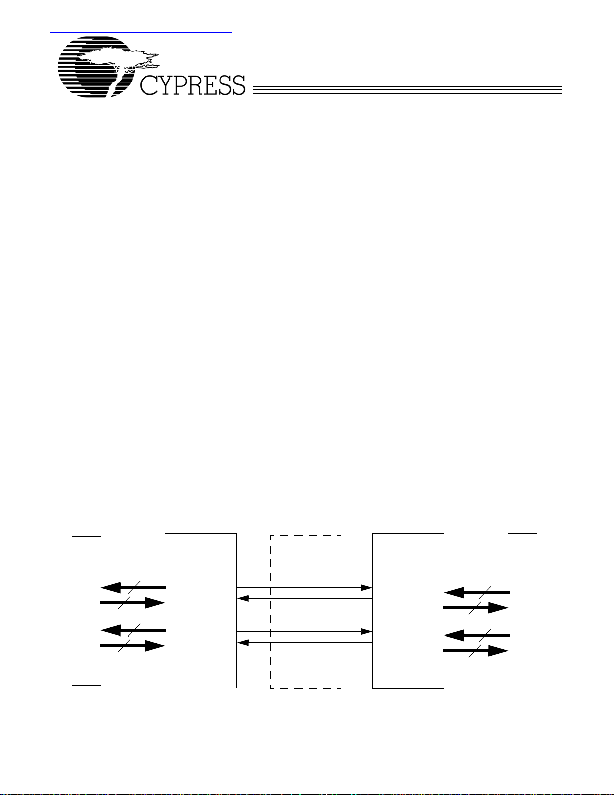
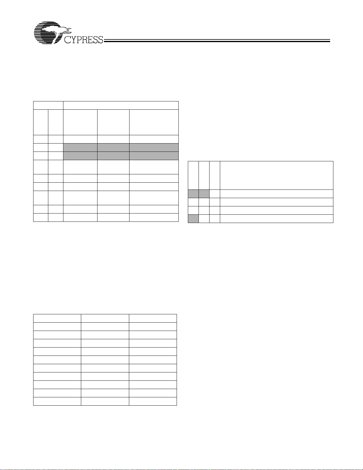
Dual-channel HOTLink II™
10
10
10
10
CYP(V)(W)15G0201DXB
System Host
Serial Links
Serial Links
Backplane or
Cabled
Connections
CYP(V)(W)15G0201DXB
10
10
10
10
System Host
Figure 1. HOTLink II™ System Connections
Note:
1. CYV15G0201DXB refers to SMPTE 259M and SMPTE 292M compliant devices. CYW15G0201DXB refers to OBSAI RP3 compliant devices (maximum
operating data rate is 1540 MBaud). CYP15G0201DXB refers to devices not compliant to SMPTE 259M and SMPTE 292M pathological test requirements and
also OBSAI RP3 operating datarate of 1536 MBaud. CYP(V)(W)15G0201DXB refers to all three devices.
Cypress Semiconductor Corporation • 3901 North First Street • San Jose, CA 95134 • 408-943-2600
Document #: 38-02058 Rev. *H Revised March 25, 2005
Page 2

CYP15G0201DXB
CYV15G0201DXB
CYW15G0201DXB
The CYW15G0201DXB
which includes operation at the OBSAI RP3 datarate of both
1536 MBaud and 768 MBaud.
The two channels may be combined to allow transport of wide
buses across significant distances with minimal concern for
offsets in clock phase or link delay. Each transmit channel
accepts parallel characters in an Input Register, encodes each
character for transport, and converts it to serial data. Each
receive channel accepts serial data and converts it to parallel
data, decodes the data into characters, and presents these
characters to an Output Register. Figure 1 illustrates typical
connections between independent host systems and corresponding CYP(V)(W)15G0201DXB parts. As a second-generation HOTLink device, the CYP(V)(W)15G0201DXB extends
the HOTLink family with enhanced levels of integration and
faster data rates, while maintaining serial-link compatibility
(data, command, and BIST) with other HOTLink devices.
The transmit (TX) section of the CYP(V)(W)15G0201DXB
Dual HOTLink II consists of two byte-wide channels that can
be operated independently or bonded to form wider buses.
Each channel can accept either 8-bit data characters or
pre-encoded 10-bit transmission characters. Data characters
are passed from the Transmit Input Register to an embedded
8B/10B Encoder to improve their serial transmission characteristics. These encoded characters are then serialized and
output from dual Positive ECL (PECL) compatible differential
transmission-line drivers at a bit-rate of either 10 or 20 times
the input reference clock.
The receive (RX) section of the CYP(V)(W)15G0201DXB Dual
HOTLink II consists of two byte-wide channels that can be
operated independently or synchronously bonded for greater
bandwidth. Each channel accepts a serial bit-stream from one
of two PECL-compatible differential line receivers and, using
a completely integrated PLL Clock Synchronizer, recovers the
timing information necessary for data reconstruction. Each
recovered bit-stream is deserialized and framed into
characters, 8B/10B decoded, and checked for transmission
[1]
operates from 195 to 1540 MBaud,
errors. Recovered decoded characters are then written to an
internal Elasticity Buffer, and presented to the destination host
system. The integrated 8B/10B Encoder/Decoder may be
bypassed for systems that present externally encoded or
scrambled data at the parallel interface.
For those systems using buses wider than a single byte, the
two independent receive paths can be bonded together to
allow synchronous delivery of data across a two-byte-wide
(16-bit) path.
The parallel I/O interface may be configured for numerous
forms of clocking to provide the highest flexibility in system
architecture. In addition to clocking the transmit path interfaces
from one of multiple sources, the receive interface may be
configured to present data relative to a recovered clock or to a
local reference clock.
Each transmit and receive channel contains independent
Built-In Self-Test (BIST) pattern generators and checkers. This
BIST hardware allows at-speed testing of the high-speed
serial data paths in each transmit and receive section, and
across the interconnecting links.
HOTLink II devices are ideal for a variety of applications where
parallel interfaces can be replaced with high-speed,
point-to-point serial links. Some applications include
interconnecting backplanes on switches, routers,
base-stations, servers and video transmission systems.
The CYV15G0201DXB is verified by testing to be compliant to
all the pathological test patterns, documented in SMPTE
EG34-1999 for both the SMPTE 259M and 292M signaling
rates. The tests ensure that the receiver recovers data with no
errors for the following patterns:
1. Repetitions of 20 ones and 20 zeros.
2. Single burst of 44 ones or 44 zeros.
3. Repetitions of 19 ones followed by 1 zero or 19 zeros
followed by 1 one.
Document #: 38-02058 Rev. *H Page 2 of 46
Page 3
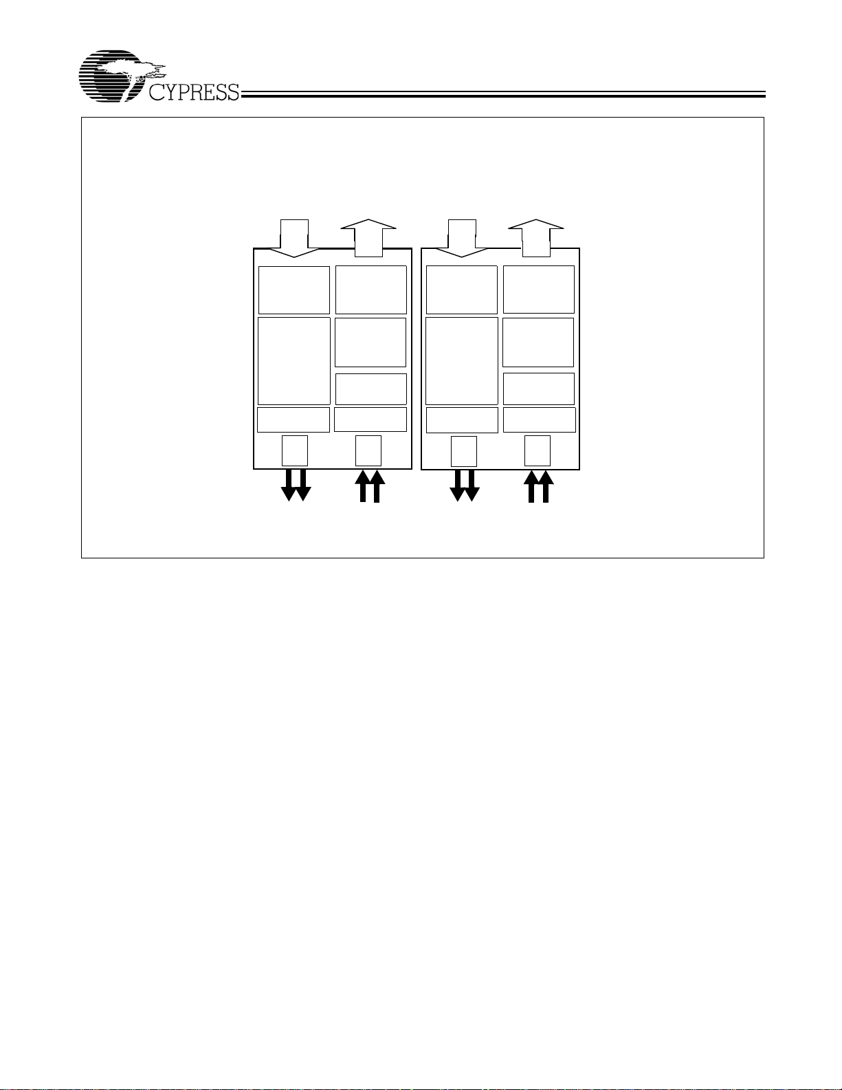
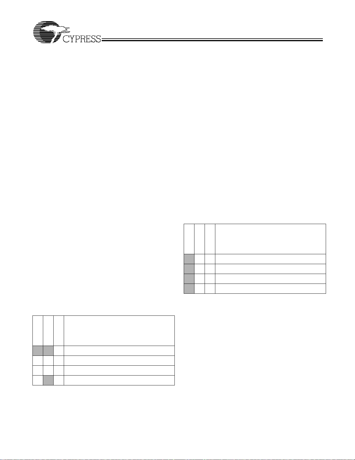
Transceiver Logic Block Diagram
TXDA[7:0]
TXCTA[1:0]
x10
RXDA[7:0]
RXSTA[2:0]
x11
TXDB[7:0]
TXCTB[1:0]
x10
RXDB[7:0]
RXSTB[2:0]
x11
CYP15G0201DXB
CYV15G0201DXB
CYW15G0201DXB
Phase
Align
Buffer
Encoder
8B/10B
Serializer
TX
OUTA1±
OUTA2±
Elasticity
Buffer
Decoder
8B/10B
Framer
Deserializer
RX
INA1±
INA2±
Phase
Align
Buffer
Encoder
8B/10B
Serializer
TX
OUTB1±
OUTB2±
Elasticity
Buffer
Decoder
8B/10B
Framer
Deserializer
RX
INB1±
INB2±
Document #: 38-02058 Rev. *H Page 3 of 46
Page 4

CYP15G0201DXB
CYV15G0201DXB
CYW15G0201DXB
Pin Configuration (Top View)
[2]
1 2 3 4 5 6 7 8 9 10 11 12 13 14
V
INA2+ OUTA2– V
CC
INA1+ OUTA1– V
CC
CC
V
INB2+ OUTB2– V
CC
INB1+ OUTB1– V
CC
A
TDO INA2– OUTA2+ V
INA1– OUTA1+ NC NC INB2– OUTB2+ V
CC
INB1– OUTB1+ BOE[3]
CC
B
NC RFEN V
LPEN RXLE RXRATE GND GND SPDSEL PARCTL RFMODE V
CC
SDASEL BOE[2]
CC
C
V
CC
V
CC
NC TXRATE RXMODE[1]RXMODE[0]GND GND TCLK TDI INSELB INSELA V
CC
D
BISTLE FRAMCHARTXMODE[1]TXMODE[0]BOE[0] BOE[1] GND GND TXOPB TXPERB TXCKSEL RXCKSEL TRSTZ TMS
E
DECMODEOELE RXCLKC+ RXSTA[2] RXSTA[1] GNDGNDGNDGNDTXDB[4] TXDB[3] TXDB[2] TXDB[1] TXDB[0]
F
V
CC
NC GNDGNDGNDGNDGNDGNDGNDGNDGNDGND NC V
G
V
CC
NC GNDGNDGNDGNDGNDGNDGNDGNDGNDGND NC V
H
RXSTA[0] RXOPA RXDA[0] RXDA[1] RXDA[2] GNDGNDGNDGNDTXCTB[0] TXCTB[1] TXDB[7] TXDB[6] TXDB[5]
J
RXDA[3] RXDA[4] RXDA[5] RXDA[6] TXDA[4] TXCLKA GND GND NC RXOPB RXCLKB+ RXCLKB- LFIB TXCLKB
K
V
CC
V
RXDA[7] LFIA TXDA[3] TXOPA GND GND SCSEL RXSTB[2] RXSTB[1] RXDB[7] V
CC
CC
L
RXCLKA- TXCTA[1] V
CC
NC TXDA[2] TXPERA GND GND TXRST NC RXSTB[0] V
RXDB[5] RXDB[6]
CC
M
RXCLKA+ TXCTA[0] TXDA[6] V
TXDA[1] NC NC NC REFCLK- TXCLKO+ V
CC
RXDB[2] RXDB[3] RXDB[4]
CC
N
V
TXDA[7] TXDA[5] V
CC
TXDA[0] NC V
CC
CC
V
REFCLK+ TXCLKO- V
CC
RXDB[1] RXDB[0] V
CC
P
Note:
2. NC = Do not connect.
CC
V
CC
CC
CC
V
CC
CC
Document #: 38-02058 Rev. *H Page 4 of 46
Page 5

CYP15G0201DXB
CYV15G0201DXB
CYW15G0201DXB
Pin Configuration (Bottom View)
[2]
14 13 12 11 10 9 8 7 6 5 4 3 2 1
V
OUTB1– INB1+ V
CC
BOE[3] OUTB1+ INB1– V
BOE[2] SDASEL V
V
TMS TRSTZ RXCKSEL TXCKSEL TXPERB TXOPB GND GND BOE[1] BOE[0] TXMODE[0] TXMODE[1]FRAMCHAR BISTLE
TXDB[0] TXDB[1] TXDB[2] TXDB[3] TXDB[4] GNDGNDGNDGNDRXSTA[1] RXSTA[2] RXCLKC+ OELE DECMODE
V
V
TXDB[5] TXDB[6] TXDB[7] TXCTB[1] TXCTB[0] GNDGNDGNDGNDRXDA[2] RXDA[1] RXDA[0] RXOPA RXSTA[0]
TXCLKB LFIB RXCLKB- RXCLKB+ RXOPB NC GND GND TXCLKA TXDA[4] RXDA[6] RXDA[5] RXDA[4] RXDA[3]
V
RXDB[6] RXDB[5] V
RXDB[4] RXDB[3] RXDB[2] VCCTXCLKO+ REFCLK- NC NC NC TXDA[1] V
V
V
CC
CC
CC
CC
CC
CC
NC GND GND GND GND GND GND GND GND GND GND NC V
NC GND GND GND GND GND GND GND GND GND GND NC V
V
CC
RXDB[0] RXDB[1] V
INSELA INSELB TDI TCLK GND GND RXMODE[0] RXMODE[1] TX RA TE N C V
RXDB[7] RXSTB[1] RXSTB[2] SCSEL GND GND TXOPA TXDA[3] LFIA RXDA[7] V
RFMODE PARCTL SPDSEL GND GND RXRATE RXLE LPEN V
CC
RXSTB[0] NC TXRST GND GND TXPERA TXDA[2] NC V
CC
OUTB2– INB2+ V
CC
OUTB2+ INB2– NC NC OUTA1+ INA1– V
CC
TXCLKO- REFCLK+ V
CC
CC
CC
V
OUTA1– INA1+ V
CC
V
CC
NC TXDA[0] V
OUTA2– INA2+ V
CC
OUTA2+ INA2– TDO
CC
RFEN NC
CC
TXCTA[1] RXCLKA-
CC
TXDA[6] TXCTA[0] RXCLKA+
CC
TXDA[5] TXDA[7] V
CC
CC
CC
CC
V
CC
CC
CC
V
CC
CC
A
B
C
D
E
F
G
H
J
K
L
M
N
P
Document #: 38-02058 Rev. *H Page 5 of 46
Page 6
CYP15G0201DXB
CYV15G0201DXB
CYW15G0201DXB
Pin Descriptions CYP(V)(W)15G0201DXB Dual HOTLink II Transceiver
Pin Name I/O Characteristics Signal Description
Transmit Path Data Signals
TXPERA
TXPERB
TXCTA[1:0]
TXCTB[1:0]
TXDA[7:0]
TXDB[7:0]
TXRST
Note:
3. When REFCLK is configured for half-rate operation (TXRATE = HIGH), these inputs are sampled (or the outputs change) relative to both the rising and falling
edges of REFCLK.
LVTTL Output,
changes relative to
REFCLK↑
LVTTL Input,
synchronous,
sampled by the
selected TXCLKx↑
or REFCLK↑
LVTTL Input,
synchronous,
sampled by the
selected TXCLKx↑
or REFCLK↑
LVTTL Input,
asynchronous,
internal pull-up,
REFCLK↑
[3]
[3]
[3]
[3]
Transmit Path Parity Error. Active HIGH. Asserted (HIGH) if parity checking is enabled
and a parity error is detected at the Encoder. This output is HIGH for one transmit character
clock period to indicate detection of a parity error in the character presented to the Encoder.
If a parity error is detected, the character in error is replaced with a C0.7 character to force
a corresponding bad-character detection at the remote end of the link. This replacement
takes place regardless of the encoded/non-encoded state of the interface.
When BIST is enabled for the specific transmit channel, BIST progress is presented on
these outputs. Once every 511 character times (plus a 16-character Word Sync Sequence
when the receive channels are clocked by a common clock, i.e., RXCKSEL = LOW or
HIGH), the associated TXPERx signal pulses HIGH for one transmit-character clock period
(if RXCKSEL = MID) or seventeen transmit- character clock periods (if RXCKSEL = LOW
or HIGH) to indicate a complete pass through the BIST sequence. For RXCKSEL = LOW
or HIGH, if TXMODE[1:0] = LL, then no Word Sync Sequence is sent in BIST, and TXPERx
pulses HIGH for one transmit-character clock period.
These outputs also provide indication of a transmit Phase-Align Buffer underflow or
overflow. When the transmit Phase-Align Buffers are enabled (TXCKSEL ≠ LOW, or
TXCKSEL = LOW and TXRATE = HIGH), if an underflow or overflow condition is detected,
TXPERx for the channel in error is asserted and remains asserted until either an atomic
Word Sync Sequence is transmitted or TXRST
Phase-Align Buffers.
Transmit Co ntrol. These inputs are captured on the rising edge of the transmit interface
clock as selected by TXCKSEL, and are passed to the Encoder or Transmit Shifter. They
identify how the associated TXDx[7:0] characters are interpreted. When the Encoder is
bypassed, these inputs are interpreted as data bits. When the Encoder is enabled, these
inputs determine if the TXDx[7:0] character is encoded as Data, a Special Character code,
or replaced with other Special Character codes. See Table 1 for details.
Transmit Data Inputs. These inputs are captured on the rising edge of the transmit
interface clock (selected by TXCKSEL) and passed to the Encoder or Transmit Shifter.
When the Encoder is enabled (TXMODE[1:0] ≠ LL), TXDx[7:0] specify the specific data or
command character to be sent.
When the Encoder is bypassed, these inputs are interpreted as data bits of the 10-bit input
character. See Tabl e 1 for details.
Transmit Clock Phase Reset. Transmit Clock Phase Reset. Active LOW. When sampled
LOW, the transmit Phase-align Buffers are allowed to adjust their data-transfer timing
(relative to the selected input clock) to allow clean transfer of data from the Input Register
to the Encoder or Transmit Shifter. When TXRST
relationship between the associated TXCLKx and the internal character-rate clock is fixed
and the device operates normally.
When configured for half-rate REFCLK sampling of the transmit character stream
(TXCKSEL = LOW and TXRATE = HIGH), assertion of TXRST
Phase-align buffer faults caused by highly asymmetric REFCLK periods or REFCLKs with
excessive cycle-to-cycle jitter. During this alignment period, one or more characters may be
added to or lost from all the associated transmit paths as the transmit Phase-align Buffers
are adjusted. TXRST
of REFCLK to ensure the reset operation is initiated correctly on all channels. This input is
ignored when both TXCKSEL and TXRATE are LOW, since the phase align buffer is
bypassed. In all other configurations, TXRST
to ensure proper operation of the Phase-align buffer. TXRST
presence of a valid TXCLKx and after allowing enough time for the TXPLL to lock to the
reference clock (as specified by parameter t
must be sampled LOW by a minimum of two consecutive rising edges
is sampled LOW to re-center the transmit
is sampled HIGH, the internal phase
is only used to clear
should be asserted during device initialization
should be asserted after
).
TXLOCK
Document #: 38-02058 Rev. *H Page 6 of 46
Page 7
CYP15G0201DXB
CYV15G0201DXB
CYW15G0201DXB
Pin Descriptions CYP(V)(W)15G0201DXB Dual HOTLink II Transceiver (continued)
Pin Name I/O Characteristics Signal Description
SCSEL LVTTL Input,
synchronous,
internal pull-down,
sampled by
TXOPA
TXOPB
TXCLKA↑
or REFCLK↑
LVTTL Input,
synchronous,
[3]
internal pull-up,
sampled by the
respective TXCLKx↑
or REFCLK↑
[3]
Transmit Path Clock and Clock Control
TXCKSEL 3-Level Select
Static Control Input
TXRATE LVTTL Input,
Static Control input,
internal pull-down
TXCLKO± LVTTL Output Transmit Clock Output. This true and complement output clock is synthesized by the
TXCLKA
TXCLKB
LVTTL Clock Input,
internal pull-down
Transmit Path Mode Control
TXMODE[1:0] 3-Level Select
Static Control inputs
Receive Path Data Signals
RXDA[7:0]
RXDB[7:0]
LVTTL Output,
synchronous to the
selected RXCLKx↑
output or
REFCLK↑
Note:
4. 3-Level select inputs are used for static configuration. They are ternary (not binary) inputs that make use of non-standard logic levels of LOW, MID, and HIGH.
The LOW level is usually implemented by direct connection to V
not connected or allowed to float, a 3-Level select input will self-bias to the MID level.
[3]
input
Special Character Select. Used in some transmit modes along with TXCTx[1:0] to encode
special characters or to initiate a Word Sync Sequence. When the transmit paths are
configured for independent inputs clocks (TXCKSEL = MID), SCSEL is captured relative to
TXCLKA↑.
Transmit Path Odd Parity. When parity checking is enabled (PARCTL ≠ LOW), the parity
captured at these inputs is XORed with the data on the associated transmit data TXDx bus
to verify the integrity of the captured character.
[4]
Transmit Clock Select. Selects the clock source, used to write data into the Transmit Input
Register, of the transmit channel(s).
When LOW, both Input Registers are clocked by REFCLK↑
[3]
. When MID, TXCLKx↑ is used
as the Input Register clock for TXDx[7:0] and TXCTx[1:0]. When HIGH, TXCLKA↑ is used
to clock data into the Input Register of each channel.
When TXCKSEL = MID or HIGH (TXCLKx or TXCLKA selected to clock input register),
configuring TXRATE = HIGH (Half-rate REFCLK) is an invalid mode of operation.
Transmit PLL Clock Rate Select. When TXRATE = HIGH, the Transmit PLL multiplies
REFCLK by 20 to generate the serial symbol-rate clock. When TXRATE = LOW, the transmit
PLL multiples REFCLK by 10 to generate the serial symbol-rate clock. See Ta ble 1 0 for a
list of operating serial rates.
When REFCLK is selected to clock the receive parallel interfaces (RXCKSEL = LOW), the
TXRATE input also determines if the clocks on the RXCLKA± and RXCLKC± outputs are
full or half-rate. When TXRATE = HIGH (REFCLK is half-rate), the RXCLKA± and RXCLKC±
output clocks are also half-rate clocks and follow the frequency and duty cycle of the
REFCLK input. When TXRATE = LOW (REFCLK is full-rate), the RXCLKA± and RXCLKC±
output clocks are full-rate clocks and follow the frequency and duty cycle of the REFCLK
input.
When TXCKSEL = MID or HIGH (TXCLKx or TXCLKA selected to clock input register),
configuring TXRATE = HIGH (Half-rate REFCLK) is an invalid mode of operation.
transmit PLL and operates synchronous to the internal transmit character clock. It operates
at either the same frequency as REFCLK (when TXRATE = LOW), or at twice the frequency
of REFCLK (when TXRATE = HIGH). This output clock has no direct phase relationship to
REFCLK.
Transmit Path Input Clocks. These clocks must be frequency-coherent to TXCLKO±, but
may be offset in phase. The internal operating phase of each input clock (relative to
REFLCK or TXCLKO±) is adjusted when TXRST = LOW and locked when TXRST =HIGH.
[4]
Transmit Operating Mode. These inputs are interpreted to select one of nine operating
modes of the transmit path. See Tab le 3 for a list of operating modes.
Parallel Data Output. These outputs change following the rising edge of the selected
receive interface clock.
When the Decoder is enabled (DECMODE = HIGH or MID), these outputs represent either
received data or special characters. The status of the received data is represented by the
values of RXSTx[2:0]. When the Decoder is bypassed (DECMODE = LOW), RXDx[7:0]
become the higher order bits of the 10-bit received character. See Table 16 for details.
(ground). The HIGH level is usually implemented by direct connection to VCC (power). When
SS
Document #: 38-02058 Rev. *H Page 7 of 46
Page 8

Pin Descriptions CYP(V)(W)15G0201DXB Dual HOTLink II Transceiver (continued)
Pin Name I/O Characteristics Signal Description
RXSTA[2:0]
RXSTB[2:0]
RXOPA
RXOPB
Receive Path Clock and Clock Control
RXRATE LVTTL Input
RXCLKA±
RXCLKB±
RXCKSEL 3-Level Select
LVTTL Output,
synchronous to the
selected RXCLKx↑
output or
REFCLK↑
3-state, LVTTL
Output, synchronous
to the selected
RXCLKx↑ output or
REFCLK↑
Static Control Input,
internal pull-down
3-state, LVTTL
Output clock or
Static control input
Static Control Input
[3]
[3]
input
input
[4]
Parallel Status Output. These outputs change following the rising edge of the selected
receive interface clock.
When the Decoder is bypassed (DECMODE = LOW), RXSTx[1:0] become the two
low-order bits of the 10-bit received character, while RXSTx[2] = HIGH indicates the
presence of a Comma character in the Output Register. See Tabl e 1 6 for details.
When the Decoder is enabled (DECMODE = HIGH or MID), RXSTx[2:0] provide status of
the received signal. See Table 18, Ta bl e 19 and Tab le 20 for a list of Receive Character
status.
Receive Path Odd Parity. When parity generation is enabled (PARCTL ≠ LOW), the parity
output at these pins is valid for the data on the associated RXDx bus bits. When parity
generation is disabled (PARCTL = LOW) these output drivers are disabled (High-Z).
Receive Clock Rate Select. When LOW, the RXCLKx± recovered clock outputs are
complementary clocks operating at the recovered character rate. Data for the associated
receive channels should be latched on the rising edge of RXCLKx+ or falling edge of
RXCLKx–. When HIGH, the RXCLKx± recovered clock outputs are complementary clocks
operating at half the character rate. Data for the associated receive channels should be
latched alternately on the rising edge of RXCLKx+ and RXCLKx–.
When REFCLK± is selected to clock the output registers (RXCKSELx = LOW), RXRATEx
is not interpreted. The RXCLKA± and RXCLKC± output clocks will follow the frequency and
duty cycle of REFCLK±.
Receive Character Clock Output or Clock Select Input. When configured such that all
output data paths are clocked by the recovered clock (RXCKSEL = MID), these true and
complement clocks are the receive interface clocks which are used to control timing of
output data (RXDx[7:0], RXSTx[2:0] and RXOPx). These clocks are output continuously at
either the dual-character rate (1/20
serial symbol-rate) of the data being received, as selected by RXRATE.
When configured such that all output data paths are clocked by REFCLK instead of a
recovered clock (RXCKSEL = LOW), the RXCLKA± and RXCLKC+ output drivers present
a buffered and delayed form of REFCLK. RXCLKA± and RXCLKC+ are buffered forms of
REFCLK that are slightly different in phase. This phase difference allows the user to select
the optimal setup/hold timing for their specific interface.
When RXCKSEL = HIGH and dual-channel bonding is enabled, one of the recovered clocks
from channels A or B is selected to present bonded data from channels A and B. RXCLKA±
output the recovered clock from either receive channel A or receive channel B as selected
by RXCLKB+ to clock the bonded output data from channels A and B. See Table 14 for
details.
When RXCKSEL = LOW and dual-channel bonding is enabled, REFCLK is selected to
present bonded data from channels A and B. RXCLKA± and RXCLKC+ output drivers
present a buffered and delayed form of REFCLK. The master channel for bonding is
selected by RXCLKB+ (which acts as an input in this mode) to clock the bonded output data
from channels A and B. See Ta bl e 1 4 for details.
Receive Clock Mode. Selects the receive clock-source used to transfer data to the Output
Registers.
When LOW, both Output Registers are clocked by REFCLK. RXCLKB± outputs are disabled
(High-Z), and RXCLKA± and RXCLKC+ present buffered and delayed forms of REFCLK.
When MID, each RXCLKx± output follows the recovered clock for the respective channel,
as selected by RXRATE. When the 10B/8B Decoder and Elasticity Buffer are bypassed
(DECMODE = LOW), RXCKSEL must be MID.
When HIGH, and channel bonding is enabled in dual-channel mode (RX modes 2 and 3),
RXCLKA± outputs the recovered clock from either receive channel A or receive channel B
as selected by RXCLKB+. These output clocks may operate at the character-rate or half the
character-rate as selected by RXRATE.
th
the serial symbol-rate) or character rate (1/10th the
CYP15G0201DXB
CYV15G0201DXB
CYW15G0201DXB
Document #: 38-02058 Rev. *H Page 8 of 46
Page 9

Pin Descriptions CYP(V)(W)15G0201DXB Dual HOTLink II Transceiver (continued)
Pin Name I/O Characteristics Signal Description
DECMODE 3-Level Select
Static Control Input
RXMODE[1:0]3-Level Select
Static Control Inputs
RFEN LVTTL input,
asynchronous,
internal pull-down
RFMODE 3-Level Select
Static Control Input
FRAMCHAR 3-Level Select
Static Control Input
Device Control Signals
PARCTL 3-Level Select
Static Control Input
[4]
Decoder Mode Select. This input selects the behavior of the Decoder block.
When LOW, the Decoder is bypassed and raw 10-bit characters are passed to the Output
Register. When the Decoder is bypassed, RXCKSEL must be MID.
When MID, the Decoder is enabled and the Cypress Decoder table for Special Code
characters is used. When HIGH, the Decoder is enabled and the alternate Decoder table
for Special Code characters is used. See Table 25 for a list of the Special Codes supported
in both encoded modes.
[4]
Receive Operating Mode. These inputs are interpreted to select one of nine operating
modes of the receive path. See Table 13 for details.
Reframe Enable for All Channels. Active HIGH. When HIGH, the framers in both channels
are enabled to frame per the presently enabled framing mode and selected framing
character.
[4]
Reframe Mode Select. Used to control the type of character framing used to adjust the
character boundaries (based on detection of one or more framing characters in the received
serial bit stream). This signal operates in conjunction with the presently enabled channel
bonding mode, and the type of framing character selected.
When LOW, the low-latency framer is selected. This will frame on each occurrence of the
selected framing character(s) in the received data stream. This mode of framing stretches
the recovered clock for one or multiple cycles to align that clock with the recovered data.
When MID, the Cypress-mode multi-byte parallel framer is selected. This requires a pair of
the selected framing character(s), on identical 10-bit boundaries, within a span of 50 bits,
before the character boundaries are adjusted. The recovered character clock remains in the
same phasing regardless of character offset.
When HIGH, the alternate mode multi-byte parallel framer is selected. This requires
detection of the selected framing character(s) of the allowed disparities in the received serial
bit stream, on identical 10-bit boundaries, on four directly adjacent characters. The
recovered character clock remains in the same phasing regardless of character offset.
[4]
Framing Character Select. Used to control the character or portion of a character used for
character framing of the received data streams.
When MID, the framer looks for both positive and negative disparity versions of the 8-bit
Comma character. When HIGH, the framer looks for both positive and negative disparity
versions of the K28.5 character. Configuring FRAMCHAR to LOW is reserved for
component test.
[4]
Parity Check/Generate Control. Used to control the different parity check and generate
functions.
When LOW, parity checking is disabled, and the RXOPx outputs are all disabled (High-Z).
When MID, and the Encoder/Decoder are enabled (TXMODE[1] ≠ LOW,
DECMODE ≠ LOW), TXDx[7:0] inputs are checked (along with TXOPx) for valid ODD parity,
and ODD parity is generated for the RXDx[7:0] outputs and presented on RXOPx. When
the Encoder and Decoder are disabled (TXMODE[1] = LOW, DECMODE = LOW), the
TXDx[7:0] and TXCTx[1:0] inputs are checked (along with TXOPx) for valid ODD parity, and
ODD parity is generated for the RXDx[7:0] and RXSTx[1:0] outputs and presented on
RXOPx. When HIGH, parity checking and generation are enabled. The TXDx[7:0] and
TXCTx[1:0] inputs are checked (along with TXOPx) for valid ODD parity, and ODD parity is
generated for the RXDx[7:0] and RXSTx[2:0] outputs and presented on RXOPx.
CYP15G0201DXB
CYV15G0201DXB
CYW15G0201DXB
Document #: 38-02058 Rev. *H Page 9 of 46
Page 10
Pin Descriptions CYP(V)(W)15G0201DXB Dual HOTLink II Transceiver (continued)
Pin Name I/O Characteristics Signal Description
REFCLK± Differential LVPECL
or single-ended
LVTTL input clock
RXCLKC+ 3-state LVTTL
SPDSEL 3-Level Select
TRSTZ
Analog I/O and Control
OUTA1±
OUTB1±
OUTA2±
OUTB2±
INA1±
INB1±
INA2±
INB2±
INSELA
INSELB
SDASEL 3-Level Select
LPEN LVTTL Input,
Output
static control input
LVTTL Input,
internal pull-up
CML Differential
Output
CML Differential
Output
LVPECL Differential
Input
LVPECL Differential
Input
LVTTL Input,
asynchronous
static configuration
input
asynchronous,
internal pull-down
Reference Clock. This clock input is used as the timing reference for the transmit and
receive PLLs. This input clock may also be selected to clock the transmit and receive parallel
interfaces. When driven by a single-ended LVCMOS or LVTTL clock source, connect the
clock source to either the true or complement REFCLK input, and leave the alternate
REFCLK input open (floating). When driven by an LVPECL clock source, the clock must be
a differential clock, using both inputs. When TXCKSEL = LOW, REFCLK is also used as the
clock for the parallel transmit data (input) interface. When RXCKSEL = LOW, the Elasticity
Buffer is enabled and REFCLK is used as the clock for the parallel receive data (output)
interface.
If the Elasticity Buffer is used, framing characters will be inserted or deleted to/from the data
stream to compensate for frequency differences between the reference clock and recovered
clock. When addition happens, a K28.5 will be appended immediately after a framing
character is detected in the Elasticity Buffer. When deletion happens, a framing character
will be removed from the datastream when detected in the Elasticity Buffer.
Delayed REFCLK+ when RXCKSEL=LOW. Delayed form of REFCLK+, used for transfer
of recovered data to a host system. This output is only enabled when the receive parallel
interface is configured to present data relative to REFCLK (RXCKSEL = LOW).
[4]
,
Serial Rate Select. This input specifies the operating bit-rate range of both transmit and
receive PLLs. LOW = 195–400 MBaud, MID = 400–800 MBaud, HIGH = 800–1500 MBaud
(800–1540 MBaud for CYW15G0201DXB). When SPDSEL is LOW, setting TXRATE =
HIGH (Half-rate Reference Clock) is invalid.
Device Reset. Active LOW. Initializes all state machines and counters in the device.
When sampled LOW by the rising edge of REFLCK, this input resets the internal state
machines and sets the Elasticity Buffer pointers to a nominal offset. When the reset is
removed (TRSTZ
deterministic in less than 16 REFCLK cycles.
The BISTLE, OELE, and RXLE latches are reset by TRSTZ.
If the Elasticity Buffer or the Phase Align Buffer are used, TRSTZ
power up to initialize the internal pointers into these memory arrays.
Primary Differential Serial Data Outputs. These PECL-compatible CML outputs (+3.3V
referenced) are capable of driving terminated transmission lines or standard fiber-optic
transmitter modules.
Secondary Differential Serial Data Outputs. These PECL-compatible CML outputs
(+3.3V referenced) are capable of driving terminated transmission lines or standard
fiber-optic transmitter modules.
Primary Differential Serial Data Inputs. These inputs accept the serial data stream for
deserialization and decoding. The INx1± serial streams are passed to the receiver Clock
and Data Recovery (CDR) circuits to extract the data content when INSELx = HIGH.
Secondary Differential Serial Data Inputs. These inputs accept the serial data stream for
deserialization and decoding. The INx2± serial streams are passed to the receiver Clock
and Data Recovery (CDR) circuits to extract the data content when INSELx = LOW.
Receive Input Selector. Determines which external serial bit stream is passed to the
receiver Clock and Data Recovery circuit. When HIGH, the INx1± input is selected. When
LOW, the INx2± input is selected.
[4]
,
Signal Detect Amplitude Level Select. Allows selection of one of three predefined
amplitude trip points for a valid signal indication, as listed in Table 11.
All-Port Loop-Back-Enable. Active HIGH. When asserted (HIGH), the transmit serial data
from each channel is internally routed to the associated receiver Clock and Data Recovery
(CDR) circuit. All serial drivers are forced to differential logic “1”. All serial data inputs are
ignored.
sampled HIGH by REFCLK↑), the status and data outputs will become
CYP15G0201DXB
CYV15G0201DXB
CYW15G0201DXB
should be applied after
Document #: 38-02058 Rev. *H Page 10 of 46
Page 11
Pin Descriptions CYP(V)(W)15G0201DXB Dual HOTLink II Transceiver (continued)
Pin Name I/O Characteristics Signal Description
OELE LVTTL Input,
asynchronous,
internal pull-up
RXLE LVTTL Input,
asynchronous,
internal pull-up
BISTLE LVTTL Input,
BOE[3:0] LVTTL Input,
LFIA
LFIB
JTAG Interface
TMS LVTTL Input,
TCLK LVTTL Input,
TDO 3-State
TDI LVTTL Input,
Power
V
CC
GND Signal and Power Ground for all internal circuits.
asynchronous,
internal pull-up
asynchronous,
internal pull-up
LVTTL Output,
Asynchronous
internal pull-up
internal pull-down
LVTTL Output
internal pull-up
Serial Driver Output Enable Latch Enable. Active HIGH. When OELE = HIGH, the signals
on the BOE[3:0] inputs directly control the OUTxy± differential drivers. When the BOE[x]
input is HIGH, the associated OUTxy± differential driver is enabled. When the BOE[x] input
is LOW, the associated OUTxy± differential driver is powered down. When OELE returns
LOW, the last values present on BOE[3:0] are captured in the internal Output Enable Latch.
The specific mapping of BOE[3:0] signals to transmit output enables is listed in Tab le 9 .
If the device is reset (TRSTZ
Receive Channel Power-Control Latch Enable. Active HIGH. When RXLE = HIGH, the
signals on the BOE[3:0] inputs directly control the power enables for the receive PLLs and
analog logic. When the BOE[3:0] input is HIGH, the associated receive channel A and
receive channel B PLL and analog logic are active. When the BOE[3:0] input is LOW, the
associated receive channel A and receive channel B PLL and analog logic are placed in a
non-functional power saving mode. When RXLE returns LOW, the last values present on
BOE[3:0] are captured in the internal RX PLL Enable Latch. The specific mapping of
BOE[3:0] signals to the associated receive channel enables is listed in Ta bl e 9 . When the
device is reset (TRSTZ
Transmit and Receive BIST Latch Enable. Active HIGH. When BISTLE = HIGH, the
signals on the BOE[3:0] inputs directly control the transmit and receive BIST enables. When
the BOE[x] input is LOW, the associated transmit or receive channel is configured to
generate or compare the BIST sequence. When the BOE[x] input is HIGH, the associated
transmit or receive channel is configured for normal data transmission or reception. When
BISTLE returns LOW, the last values present on BOE[3:0] are captured in the internal BIST
Enable Latch. The specific mapping of BOE[3:0] signals to transmit and receive BIST
enables is listed in Table 9. When the latch is closed, if the device is reset (TRSTZ
LOW), the latch is reset to disable BIST on all transmit and receive channels.
BIST, Serial Output, and Receive Channel Enables. These inputs are passed to and
through the Output Enable Latch when OELE = HIGH, and captured in this latch when
OELE returns LOW. These inputs are passed to and through the BIST Enable Latch when
BISTLE = HIGH, and captured in this latch when BISTLE returns LOW. These inputs are
passed to and through the Receive Channel Enable Latch when RXLE = HIGH, and
captured in this latch when RXLE returns LOW.
Link Fault Indication Output. Active LOW. LFIx is the logical OR of four internal conditions:
1. Received serial data frequency outside expected range.
2. Analog amplitude below expected levels.
3. Transition density lower than expected.
4. Receive Channel disabled.
Test Mode Select. Used to control access to the JTAG Test Modes. If maintained HIGH for
>5 TCLK cycles, the JTAG test controller is reset. The TAP controller is also reset automatically upon application of power to the device.
JTAG Test Clock.
Test Dat a O u t . JTAG data output buffer which is High-Z while JTAG test mode is not
selected.
Test Dat a In . JTAG data input port.
+3.3V power.
is sampled LOW), the latch is reset to disable all outputs.
is sampled LOW), the latch is reset to disable both receive channels.
CYP15G0201DXB
CYV15G0201DXB
CYW15G0201DXB
is sampled
Document #: 38-02058 Rev. *H Page 11 of 46
Page 12
CYP15G0201DXB
CYV15G0201DXB
CYW15G0201DXB
CYP(V)(W)15G0201DXB HOTLink II Operation
The CYP(V)(W)15G0201DXB is a highly configurable device
designed to support reliable transfer of large quantities of data,
using high-speed serial links, from one or multiple sources to
one or multiple destinations. This device supports two
single-byte or single-character channels that may be
combined to support transfer of wider buses.
CYP(V)(W)15G0201DXB Transmit Data Path
Operating Modes
The transmit path of the CYP(V)(W)15G0201DXB supports
two character-wide data paths. These data paths are used in
multiple operating modes as controlled by the TXMODE[1:0]
inputs.
Input Register
The bits in the Input Register for each channel support
different assignments, based on if the character is unencoded,
encoded with two control bits, or encoded with three control
bits. These assignments are shown in Tab le 1 .
Each Input Register captures a minimum of eight data bits and
two control bits on each input clock cycle. When the Encoder
is bypassed, the TXCTx[1:0] control bits are part of the
pre-encoded 10-bit character.
When the Encoder is enabled (TXMODE[1] ≠ LOW), the
TXCTx[1:0] bits are interpreted along with the associated
TXDx[7:0] character to generate the specific 10-bit transmission character. When TXMODE[0] ≠ HIGH, an additional
special character select (SCSEL) input is also captured and
interpreted. This SCSEL input is used to modify the encoding
of the associated characters. When the transmit Input
Registers are clocked by a common clock (TXCLKA↑ or
REFCLK↑), this SCSEL input can be changed on a
clock-by-clock basis and affects both channels.
Table 1. Input Register Bit Assignments
Signal Name Unencoded
TXDx[0]
(LSB) DINx[0] TXDx[0] TXDx[0]
TXDx[1] DINx[1] TXDx[1] TXDx[1]
TXDx[2] DINx[2] TXDx[2] TXDx[2]
TXDx[3] DINx[3] TXDx[3] TXDx[3]
TXDx[4] DINx[4] TXDx[4] TXDx[4]
TXDx[5] DINx[5] TXDx[5] TXDx[5]
TXDx[6] DINx[6] TXDx[6] TXDx[6]
TXDx[7] DINx[7] TXDx[7] TXDx[7]
TXCTx[0] DINx[8] TXCTx[0] TXCTx[0]
TXCTx[1]
(MSB) DINx[9] TXCTx[1] TXCTx[1]
SCSEL N/A N/A SCSEL
[5]
Encoded
2-bit
Control
3-bit
Control
When operated with a separate input clock on each transmit
channel, this SCSEL input is sampled synchronous to
TXCLKA↑. While the value on SCSEL still affects both
channels, it is interpreted when the character containing it is
read from the transmit Phase-Align Buffer (where both paths
are internally clocked synchronously).
Phase-Align Buffer
Data from the Input Registers is passed either to the Encoder
or to the associated Phase-Align Buffer. When the transmit
paths are operated synchronous to REFCLK↑ (TXCKSEL =
LOW and TXRATE = LOW), the Phase-Align Buffers are
bypassed and data is passed directly to the parity check and
Encoder blocks to reduce latency.
When an Input-Register clock with an uncontrolled phase
relationship to REFCLK is selected (TXCKSEL ≠ LOW) or if
data is captured on both edges of REFCLK
(TXRATE = HIGH), the Phase-Align Buffers are enabled.
These buffers are used to absorb clock phase differences
between the presently selected input clock and the internal
character clock.
Initialization of these Phase-Align buffers takes place when the
TXRST
input is sampled by two consecutive rising edges of
REFCLK. When TXRST
clock phase relative to REFCLK↑ is set. TXRST
is returned HIGH, the present input
is an
asynchronous input, but is sampled internally to synchronize
it to the internal transmit path state machines.
Once set, the input clocks are allowed to skew in time up to
half a character period in either direction relative to REFCLK↑;
i.e., ±180°. This time shift allows the delay paths of the
character clocks (relative to REFLCK↑) to change due to
operating voltage and temperature, while not affecting the
design operation.
If the phase offset, between the initialized location of the input
clock and REFCLK↑, exceeds the skew handling capabilities
of the Phase-Align Buffer, an error is reported on the
associated TXPERx output. This output indicates a continuous
error until the Phase-Align Buffer is reset. While the error
remains active, the transmitter for the associated channel
outputs a continuous C0.7 character to indicate to the remote
receiver that an error condition is present in the link.
In specific transmit modes, it is also possible to reset the
Phase-Align Buffers individually and with minimal disruption of
the serial data stream. When the transmit interface is
configured for generation of atomic Word Sync Sequences
(TXMODE[1] = MID) and a Phase-Align Buffer error is
present, the transmission of a Word Sync Sequence will
recenter the Phase Align Buffer and clear the error condition.
[6]
Notes:
5. The TXOPx inputs are also captured in the associated Input Register, but their interpretation is under the separate control of PARCTL.
6. One or more K28.5 characters may be added or lost from the data stream during this reset operation. When used with non-Cypress devices that require a
complete 16-character Word Sync Sequence for proper receive Elasticity Buffer alignment, it is recommend that the sequence be followed by a second Word
Sync Sequence to ensure proper operation.
Document #: 38-02058 Rev. *H Page 12 of 46
Page 13
CYP15G0201DXB
CYV15G0201DXB
CYW15G0201DXB
Parity Support
In addition to the ten data and control bits that are captured at
each transmit Input Register, a TXOPx input is also available
on each channel. This allows the CYP(V)(W)15G0201DXB to
support ODD parity checking for each channel. This parity
checking is available for all operating modes (including
Encoder Bypass). The specific mode of parity checking is
controlled by the PARCTL input, and operates per Tab le 2.
Table 2. Input Register Bits Checked for Parity
Transmit Parity Check Mode (PARCTL)
MID
Signal
Name
TXDx[0] X
TXDx[1] X X X
TXDx[2] X X X
TXDx[3] X X X
TXDx[4] X X X
TXDx[5] X X X
TXDx[6] X X X
TXDx[7] X X X
TXCTx[0] X X
TXCTx[1] X X
TXOPx X X X
When PARCTL is MID (open) and the Encoders are enabled
(TXMODE[1] ≠ L), only the TXDx[7:0] data bits are checked for
ODD parity along with the associated TXOPx bit. When
PARCTL = HIGH with the Encoder enabled (or MID with the
Encoder bypassed), the TXDx[7:0] and TXCTx[1:0] inputs are
checked for ODD parity along with the associated TXOPx bit.
When PARCTL = LOW, parity checking is disabled.
When parity checking and the Encoder are both enabled
(TXMODE[1] ≠ LOW), the detection of a parity error causes a
C0.7 character of proper disparity to be passed to the Transmit
Shifter. When the Encoder is bypassed (TXMODE[1] = LOW),
detection of a parity error causes a positive disparity version
of a C0.7 transmission character to be passed to the Transmit
Shifter.
Encoder
The character, received from the Input Register or
Phase-Align Buffer and Parity Check logic, is then passed to
the Encoder logic. This block interprets each character and
any associated control bits, and outputs a 10-bit transmission
character.
Depending on the configured operating mode, the generated
transmission character may be
• the 10-bit pre-encoded character accepted in the Input
Register
• the 10-bit equivalent of the 8-bit Data character accepted in
the Input Register
• the 10-bit equivalent of the 8-bit Special Character code
accepted in the Input Register
Notes:
7. Transmit path parity errors are reported on the associated TXPERx output.
8. Bits marked as X are XORed together. Result must be a logic-1 for parity to be valid.
LOW
TXMODE[1]
= LOW
[8]
TXMODE[1]
≠ LOW
[7]
HIGH
XX
The selection of the specific characters generated is controlled
by the TXMODE[1:0], SCSEL, TXCTx[1:0], and TXDx[7:0]
inputs for each character.
Data Encoding
Raw data, as received directly from the Transmit Input
Register, is seldom in a form suitable for transmission across
a serial link. The characters must usually be processed or
transformed to guarantee
When the Encoder is enabled (TXMODE[1] ≠ LOW), the
characters to be transmitted are converted from Data or
Special Character codes to 10-bit transmission characters (as
selected by their respective TXCTx[1:0] and SCSEL inputs),
using an integrated 8B/10B Encoder. When directed to encode
the character as a Special Character code, it is encoded using
the Special Character encoding rules listed in Table 25. When
directed to encode the character as a Data character, it is
encoded using the Data Character encoding rules in Table 24.
The 8B/10B Encoder is standards compliant with ANSI/NCITS
ASC X3.230-1994 (Fibre Channel), IEEE 802.3z (Gigabit
Ethernet), the IBM
Digital Video Broadcast DVB-ASI standards for data transport.
Many of the Special Character codes listed in Table 25 may be
generated by more than one input character. The
CYP(V)(W)15G0201DXB is designed to support two
independent (but non-overlapping) Special Character code
tables. This allows the CYP(V)(W)15G0201DXB to operate in
mixed environments with other CYP(V)(W)15G0201DXBs
using the enhanced Cypress command code set, and the
reduced command sets of other non-Cypress devices. Even
when used in an environment that normally uses non-Cypress
Special Character codes, the selective use of Cypress
command codes can permit operation where running disparity
and error handling must be managed.
Following conversion of each input character from eight bits to
a 10-bit transmission character, it is passed to the Transmit
Shifter and is shifted out LSB first, as required by ANSI and
IEEE standards for 8B/10B coded serial data streams.
Transmit Modes
The operating mode of the transmit path is set through the
TXMODE[1:0] inputs. These 3-level select inputs allow one of
nine transmit modes to be selected. The transmit modes are
listed in Table 3.
• the 10-bit equivalent of the C0.7 SVS character if parity
checking was enabled and a parity error was detected
• the 10-bit equivalent of the C0.7 SVS character if a
Phase-Align Buffer overflow or underflow error is present
• a character that is part of the 511-character BIST sequence
• a K28.5 character generated as an individual character or
as part of the 16-character Word Sync Sequence.
• a minimum transition density (to allow the serial receive PLL
to extract a clock from the data stream)
• a DC-balance in the signaling (to prevent baseline wander)
• run-length limits in the serial data (to limit the bandwidth
requirements of the serial link)
• the remote receiver a way of determining the correct
character boundaries (framing).
®
ESCON® and FICON® channels, and
Document #: 38-02058 Rev. *H Page 13 of 46
Page 14
CYP15G0201DXB
CYV15G0201DXB
CYW15G0201DXB
The encoded modes (TX Modes 3 through 8) support multiple
encoding tables. These encoding tables vary by the specific
combinations of SCSEL, TXCTx[1], and TXCTx[0] that are
used to control the generation of data and control characters.
These multiple encoding forms allow maximum flexibility in
interfacing to legacy applications, while also supporting
numerous extensions in capabilities.
Table 3. Transmit Operating Modes
TX Mode Operating Mode
Word Sync
Mode
Number
[1:0]
TXMODE
Sequence
Support
SCSEL
Control TXCTx Function
0 LL None None Encoder Bypass
1LM
2LH
3 ML Atomic Special
None None Reserved for test
None None Reserved for test
Encoder Control
Character
4 MM Atomic Word Sync Encoder Control
5 MH Atomic None Encoder Control
6 HL Interruptible Special
Encoder Control
Character
7 HM Interruptible Word Sync Encoder Control
8 HH Interruptible None Encoder Control
TX Mode 0—Encoder Bypass
When the Encoder is bypassed, the character captured in the
TXDx[7:0] and TXCTx[1:0] inputs is passed directly to the
Transmit Shifter without modification. If parity checking is
enabled (PARCTL ≠ LOW) and a parity error is detected, the
10-bit character is replaced with the 1001111000 pattern
(+C0.7 character).
With the Encoder bypassed, the TXCTx[1:0] inputs are
considered part of the data character and do not perform a
control function that would otherwise modify the interpretation
of the TXDx[7:0] bits. The bit usage and mapping of these
control bits when the Encoder is bypassed is shown in Table 4.
Table 4. Encoder Bypass Mode (TXMODE[1:0] = LL)
Signal Name Bus Weight 10B Name
TXDx[0]
(LSB)
[9]
TXDx[1] 2
TXDx[2] 2
TXDx[3] 2
TXDx[4] 2
TXDx[5] 2
TXDx[6] 2
TXDx[7] 2
TXCTx[0] 2
TXCTx[1]
Note:
9. LSB is shifted out first.
(MSB) 2
0
2
1
2
3
4
5
6
7
8
9
a
b
c
d
e
i
f
g
h
j
TX Modes 1 and 2—Factory Test Modes.
In Encoder Bypass the SCSEL input is ignored. All clocking
modes interpret the data the same, with no internal linking
between channels.
These modes enable specific factory test configurations. They
are not considered normal operating modes of the device.
Entry or configuration into these test modes will not damage
the device.
TX Mode 3—Atomic Word Sync and SCSEL Control of Special
Codes
When configured in TX Mode 3, the SCSEL input is captured
along with the associated TXCTx[1:0] data control inputs.
These bits combine to control the interpretation of the
TXDx[7:0] bits and the characters generated by them. These
bits are interpreted as listed in Table 5.
Table 5. TX Modes 3 and 6 Encoding
SCSEL
TXCTx[1]
TXCTx[0]
Characters Generated
X X 0 Encoded data character
0 0 1 K28.5 fill character
1 0 1 Special character code
X 1 1 16-character Word Sync Sequence
When TXCKSEL = MID, both transmit channels capture data
into their Input Registers using independent TXCLKx clocks.
The SCSEL input is sampled only by TXCLKA↑. When the
character (accepted in the Channel-A Input Register) has
passed through the Phase-Align Buffer and any selected parity
validation, the level captured on SCSEL is passed to the
Encoder of Channel-B during this same cycle.
To avoid the possible ambiguities that may arise due to the
uncontrolled arrival of SCSEL relative to the characters in the
alternate channel, SCSEL is often used as a static control
input.
Word Sync Sequence
When TXCTx[1:0] = 11, a 16-character sequence of K28.5
characters, known as a Word Sync Sequence, is generated on
the associated channel. This sequence of K28.5 characters
may start with either a positive or negative disparity K28.5 (as
determined by the current running disparity and the 8B/10B
coding rules). The disparity of the second and third K28.5
characters in this sequence are reversed from what normal
8B/10B coding rules would generate. The remaining K28.5
characters in the sequence follow all 8B/10B coding rules. The
disparity of the generated K28.5 characters in this sequence
would follow a pattern of either
++––+–+–+–+–+–+– or
––++–+–+–+–+–+–+.
When TXMODE[1] = MID (open, TX modes 3, 4, and 5), the
generation of this character sequence is an atomic (non-interruptible) operation. Once it has been successfully started, it
cannot be stopped until all 16 characters have been
generated. The content of the associated Input Register(s) is
ignored for the duration of this 16-character sequence.
Document #: 38-02058 Rev. *H Page 14 of 46
Page 15
CYP15G0201DXB
CYV15G0201DXB
CYW15G0201DXB
At the end of this sequence, if the TXCTx[1:0] = 11 condition
is sampled again, the sequence restarts and remains uninterruptible for the following 15 character clocks.
If parity checking is enabled, the character used to start the
Word Sync Sequence must also have correct ODD parity.
Once the sequence is started, parity is not checked on the
following 15 characters in the Word Sync Sequence.
When TXMODE[1] = HIGH (TX modes 6, 7, and 8), the generation of the Word Sync Sequence becomes an interruptible
operation. In TX Mode 6, this sequence is started as soon as
the TXCTx[1:0] = 11 condition is detected on a channel. In
order for the sequence to continue on that channel, the
TXCTx[1:0] inputs must be sampled as 00 for the remaining
15 characters of the sequence.
If at any time a sample period exists where TXCTx[1:0] ≠ 00,
the Word Sync Sequence is terminated, and a character representing the associated data and control bits is generated by
the Encoder. This resets the Word Sync Sequence state
machine such that it will start at the beginning of the sequence
at the next occurrence of TXCTx[1:0] = 11.
When parity checking is enabled and TXMODE[1] = HIGH, all
characters (including those in the middle of a Word Sync
Sequence) must have correct parity. The detection of a
character with incorrect parity during a Word Sync Sequence
(regardless of the state of TXCTx[1:0]) will interrupt that
sequence and force generation of a C0.7 SVS character. Any
interruption of the Word Sync Sequence causes the sequence
to terminate.
When TXCKSEL = LOW, the Input Registers for both transmit
channels are clocked by REFCLK
HIGH, the Input Registers for both transmit channels are
clocked with TXCLKA↑. In these clock modes both sets of
TXCTx[1:0] inputs operate synchronous to the SCSEL
[10]
input.
TX Mode 4—Atomic Word Sync and SCSEL Control of
Word Sync Sequence Generation
When configured in TX Mode 4, the SCSEL input is captured
along with the associated TXCTx[1:0] data control inputs.
These bits combine to control the interpretation of the
TXDx[7:0] bits and the characters generated by them. These
bits are interpreted as listed in Table 6.
Table 6. TX Modes 4 and 7 Encoding
SCSEL
X X 0 Encoded data character
0 0 1 K28.5 fill character
0 1 1 Special character code
1
When TXCKSEL = MID, both transmit channels operate
independently. The SCSEL input is sampled only by
Note:
10. When operated in any configuration where receive channels are bonded together, TXCKSEL must be either LOW or HIGH (not MID) to ensure that associated
TXCTx[0]
TXCTx[1]
X 1 16-character Word Sync Sequence
characters are transmitted in the same character cycle.
Characters Generated
[3]
. When TXCKSEL =
TXCLKA↑. When the character accepted in the Channel-A
Input Register has passed any selected validation and is ready
to be passed to the Encoder, the level captured on SCSEL is
passed to the Encoder of Channel-B during this same cycle.
Changing the state of SCSEL changes the relationship of the
characters on the alternate channel. SCSEL should either be
used as a static configuration input or changed only when the
state of TXCTx[1:0] on the alternate channel are such that
SCSEL is ignored during the change.
TX Mode 4 also supports an Atomic Word Sync Sequence.
Unlike TX Mode 3, this sequence is started when both SCSEL
and TXCTx[0] are sampled HIGH. With the exception of the
combination of control bits used to initiate the sequence, the
generation and operation of this Word Sync Sequence is the
same as that documented for TX Mode 3.
TX Mode 5—Atomic Word Sync, No SCSEL
When configured in TX Mode 5, the SCSEL signal is not used.
In addition to the standard character encodings, both with and
without atomic Word Sync Sequence generation, two
additional encoding mappings are controlled by the Channel
Bonding selection made through the RXMODE[1:0] inputs.
For non-bonded operation, the TXCTx[1:0] inputs for each
channel control the characters generated by that channel. The
specific characters generated by these bits are listed in
Tabl e 7 .
Table 7. TX Modes 5 and 8 Encoding, Non-Bonded
(RXMODE[1] = LOW)
SCSEL
X 0 0 Encoded data character
X 0 1 K28.5 fill character
X 1 0 Special character code
X 1 1 16-character Word Sync Sequence
TX Mode 5 also has the capability of generating an atomic
Word Sync Sequence. For the sequence to be started, the
TXCTx[1:0] inputs must both be sampled HIGH. With the
exception of the combination of control bits used to initiate the
sequence, the generation and operation of this Word Sync
Sequence is the same as that documented for TX Mode 3.
Two additional encoding maps are provided for use when
receive channel bonding is enabled. When dual-channel
bonding is enabled (RXMODE[1] = HIGH), the
CYP(V)(W)15G0201DXB is configured such that channels A
and B are bonded together to form a two-character-wide path.
When operated in this two-channel bonded mode, the
TXCTA[0] and TXCTB[0] inputs control the interpretation of the
data on both the A and B channels. The characters on each
half of these bonded channels are controlled by the associated
TXCTx[1] bit. The specific characters generated by these
control bit combinations are listed in Table 8.
TXCTx[0]
TXCTx[1]
Characters Generated
Document #: 38-02058 Rev. *H Page 15 of 46
Page 16

Table 8. TX Modes 5 and 8, Dual-channel Bonded (RXMODE[1] = HIGH)
CYP15G0201DXB
CYV15G0201DXB
CYW15G0201DXB
SCSEL
X0 0 X 0 Encoded data character on channel A
X0 1 X 0 K28.5 fill character on channel A
X1 0 X 0 Special character code on channel A
X1 1 X 0 16-character word sync on channel A
X X 0 0 0 Encoded data character on channel B
X X 1 0 0 K28.5 fill character on channel B
X X 0 1 0 Special character code on channel B
X X 1 1 0 16-character word sync on channel B
X X X X 1 16-character word sync on channels A and B
Note especially that any time TXCTB[0] is sampled HIGH, both
channels A and B start generating an Atomic Word Sync
Sequence, regardless of the state of any of the other bits in the
A or B Input Registers (with the exception of any enabled parity
checking).
Transmit BIST
Each transmit channel contains an internal pattern generator
that can be used to validate both device and link operation.
These generators are enabled by the associated BOE[x]
signals listed in Table 9 (when the BISTLE latch enable input
is HIGH). When enabled, a register in the associated transmit
channel becomes a signature pattern generator by logically
converting to a Linear Feedback Shift Register (LFSR). This
LFSR generates a 511-character sequence that includes all
Data and Special Character codes, including the explicit
violation symbols. This provides a predictable yet
pseudo-random sequence that can be matched to an identical
LFSR in the attached Receiver(s). If the receive channels are
configured for common clock operation (RXCKSEL ≠ MID)
and Encoder is enabled (TXMODE[1] ≠ LOW) each pass is
preceded by a 16-character Word Sync Sequence to allow
Elasticity Buffer alignment and management of clockfrequency variations.
When the BISTLE signal is HIGH, any BOE[x] input that is
LOW enables the BIST generator in the associated transmit
channel (or the BIST checker in the associated receive
channel). When BISTLE returns LOW, the values of all BOE[x]
signals are captured in the BIST Enable Latch. These values
remain in the BIST Enable Latch until BISTLE is returned
HIGH to open the latch. A device reset, (TRSTZ
LOW) presets the BIST Enable Latch to disable BIST on all
channels. All data and data-control information present at the
associated TXDx[7:0] and TXCTx[1:0] inputs are ignored
when BIST is active on that channel.
Serial Output Drivers
The serial interface Output Drivers use high-performance
differential CML (Current Mode Logic) to provide a
source-matched driver for the transmission lines. These
drivers accept data from the Transmit Shifters. These outputs
have signal swings equivalent to that of standard PECL
drivers, and are capable of driving AC-coupled optical
modules or transmission lines. To achieve OBSAI RP3
TXCTA[1]
TXCTA[0]
TXCTB[1]
TXCTB[0]
sampled
Characters Generated
compliancy, the serial output drivers must be AC-coupled to
the transmission medium.
When configured for local loopback (LPEN = HIGH), all
enabled Serial Drivers are configured to drive a static
differential logic-1.
Each Serial Driver can be enabled or disabled separately
through the BOE[3:0] inputs, as controlled by the OELE
latch-enable signal. When OELE is HIGH, the signals present
on the BOE[3:0] inputs are passed through the Serial Output
Enable Latch to control the serial output drivers. The BOE[3:0]
input associated with a specific OUTxy± driver is listed in
Tabl e 9 .
Table 9. Output Enable, BIST, and Receive Channel
Enable Signal Map
BOE
Input
BOE[3] OUTB2± Transmit B
BOE[2] OUTB1± Receive B Receive B
BOE[1] OUTA2± Transmit A
BOE[0] OUTA1± Receive A Receive A
When OELE is HIGH and BOE[x] is HIGH, the associated
Serial Driver is enabled. When OELE is HIGH and BOE[x] is
LOW, the associated driver is disabled and internally powered
down. If both outputs for a channel are in this disabled state,
the associated internal logic for that channel is also powered
down. When OELE returns LOW, the values present on the
BOE[3:0] inputs are latched in the Output Enable Latch, and
remain there until OELE returns HIGH to enable the latch. A
device reset (TRSTZ
disables all output drivers.
Note. When all transmit channels are disabled (i.e., both
outputs disabled in all channels) and a channel is re-enabled,
the data on the Serial Drivers may not meet all timing specifications for up to 200 µs.
Transmit PLL Clock Multiplier
The Transmit PLL Clock Multiplier accepts a character-rate or
half-character-rate external clock at the REFCLK input, and
multiples that clock by 10 or 20 (as selected by TXRATE) to
Output
Controlled
(OELE)
sampled LOW) clears this latch and
BIST
Channel
Enable
(BISTLE)
Receive PLL
Channel
Enable
(RXLE)
X
X
Document #: 38-02058 Rev. *H Page 16 of 46
Page 17

CYP15G0201DXB
CYV15G0201DXB
CYW15G0201DXB
generate a bit-rate clock for use by the Transmit Shifter. It also
provides a character-rate clock used by the transmit paths.
The clock multiplier PLL can accept a REFCLK input between
10 MHz and 150 MHz (19.5 MHz and 154 MHz for
CYW15G0201DXB), however, this clock range is limited by
the operating mode of the CYP(V)(W)15G0201DXB clock
multiplier (controlled by TXRATE) and by the level on the
SPDSEL input.
SPDSEL is a 3-level select
[4]
(ternary) input that selects one
of three operating ranges for the serial data outputs and inputs.
The operating serial signaling-rate and allowable range of
REFCLK frequencies are listed in Tab le 1 0.
Table 10. Operating Speed Settings
REFCLK
SPDSEL TXRATE
LOW
1 Reserved 195–400
Frequency
(MHz)
Signaling
Rate (MBaud)
0 19.5–40
MID (Open) 1 20–40 400–800
0 40–80
HIGH 1 40–75 800–1500
0 80–150
(800–1540 for
CYW15G0201
DXB)
signal of at least VI
differential. Each Line Receiver can be DC- or AC-coupled to
> 100 mV, or 200 mV peak-to-peak
DIFF
+3.3V powered fiber-optic interface modules (any ECL/PECL
logic family, not limited to 100K PECL) or AC-coupled to +5V
powered optical modules. The common-mode tolerance of
these line receivers accommodates a wide range of signal
termination voltages. Each receiver provides internal
DC-restoration, to the center of the receiver’s common mode
range, for AC-coupled signals.
The local loopback input (LPEN) allows the serial transmit data
outputs to be routed internally back to the Clock and Data
Recovery circuit associated with each channel. When
configured for local loopback, all transmit serial driver outputs
are forced to output a differential logic-1. This prevents local
diagnostic patterns from being broadcast to attached remote
receivers.
Signal Detect/Link Fault
Each selected Line Receiver (i.e., that routed to the Clock and
Data Recovery PLL) is simultaneously monitored for
• analog amplitude above limit specified by SDASEL
• transition density greater than specified limit
• range controller reports the received data stream within
normal frequency range (±1500 ppm)
[11]
• receive channel enabled
All of these conditions must be valid for the Signal Detect block
to indicate a valid signal is present. This status is presented on
When TXRATE = HIGH (Half-rate REFCLK), TXCKSEL =
HIGH or MID (TXCLKx or TXCLKA selected to clock input
register) is an invalid mode of operation.
The REFCLK± input is a differential input with each input internally biased to 1.4V. If the REFCLK+ input is connected to a
TTL, LVTTL, or LVCMOS clock source, the input signal is
recognized when it passes through the internally biased
reference point.
When both the REFCLK+ and REFCLK– inputs are
connected, the clock source must be a differential clock. This
can be either a differential LVPECL clock that is DC-or
AC-coupled, or a differential LVTTL or LVCMOS clock.
By connecting the REFCLK– input to an external voltage
source or resistive voltage divider, it is possible to adjust the
reference point of the REFCLK+ input for alternate logic levels.
When doing so it is necessary to ensure that the 0V-differential
crossing point remains within the parametric range supported
by the input.
CYP(V)(W)15G0201DXB Receive Data Path
the LFIx
receive channel, which changes synchronous to the selected
receive interface clock.
Table 11. Analog Amplitude Detect Valid Signal Levels
LOW 140 mV p-p differential
MID (Open) 280 mV p-p differential
HIGH 420 mV p-p differential
Analog Amplitude
While the majority of these signal monitors are based on fixed
constants, the analog amplitude level detection is adjustable
to allow operation with highly attenuated signals, or in
high-noise environments. This adjustment is made through the
SDASEL signal, a 3-level select
point for the detection of a valid signal at one of three levels,
as listed in Ta bl e 11 . This control input effects the analog
monitors for all receive channels.
(Link Fault Indicator) output associated with each
[12]
SDASEL Typical signal with peak amplitudes above
[4]
input, which sets the trip
The Analog Signal Detect monitors are active for the Line
Serial Line Receivers
Two differential Line Receivers, INx1± and INx2±, are
available on each channel for accepting serial data streams.
The active Serial Line Receiver on a channel is selected using
the associated INSELx input. The Serial Line Receiver inputs
are differential, and can accommodate wire interconnect and
filtering losses or transmission line attenuation greater than
Receiver, selected by the associated INSELx input. When
configured for local loopback (LPEN = HIGH), no line
receivers are selected, and the LFIx
output for each channel
reports only the receive VCO frequency out-of-range and
transition density status of the associated transmit signal.
When local loopback is active, the Analog Signal Detect
Monitors are disabled.
16 dB. For normal operation, these inputs should receive a
11. REFCLK has no phase or frequency relationship with the recovered clock(s) and only acts as a centering reference to reduce clock synchronization time. REFCLK
must be within ±1500 ppm (±0.15%) of the remote transmitter’s PLL reference (REFCLK) frequency. Although transmitting to a HOTLink II receiver necessitates
the frequency difference between the transmitter and receiver reference clocks to be within ±1500 ppm, the stability of the crystal needs to be within the limits
specified by the appropriate standard when transmitting to a remote receiver that is compliant to that standard. For example, to be IEEE 802.3z Gigabit Ethernet
compliant, the frequency stability of the crystal needs to be within ±100PPM
12. The peak amplitudes listed in this table are for typical waveforms that have generally 3–4 transitions for every ten bits. In a worse case environment the signals
may have a sign-wave appearance (highest transition density with repeating 0101...). Signal peak amplitudes levels within this environment type could increase
the values in the table above by approximately 100 mV.
Document #: 38-02058 Rev. *H Page 17 of 46
Page 18

CYP15G0201DXB
CYV15G0201DXB
CYW15G0201DXB
Transition Density
The Transition Detection logic checks for the absence of any
transitions spanning greater than six transmission characters
(60 bits). If no transitions are present in the data received on
a channel (within the referenced period), the Transition
Detection logic for that channel will assert LFIx
output remains asserted until at least one transition is detected
in each of three adjacent received characters.
Range Controls
The Clock/Data Recovery (CDR) circuit includes logic to
monitor the frequency of the Phase Locked Loop (PLL)
Voltage Controlled Oscillator (VCO) used to sample the
incoming data stream. This logic ensures that the VCO
operates at, or near the rate of the incoming data stream for
two primary cases:
• when the incoming data stream resumes after a time in
which it has been “missing”
• when the incoming data stream is outside the acceptable
frequency range
To perform this function, the frequency of the VCO is periodically sampled and compared to the frequency of the REFCLK
input. If the VCO is running at a frequency beyond
±1500 ppm
is periodically forced to the correct frequency (as defined by
REFCLK, SPDSEL, and TXRATE) and then released in an
attempt to lock to the input data stream. The sampling and
relock period of the Range Control is calculated as follows:
RANGE CONTROL SAMPLING PERIOD = (REFCLKPERIOD) * (16000).
During the time that the Range Control forces the PLL VCO to
run at REFCLK*10 (or REFCLK*20 when TXRATE = HIGH)
rate, the LFIx output will be asserted LOW. While the PLL is
attempting to re-lock to the incoming data stream, LFIx may be
either HIGH or LOW (depending on other factors such as
transition density and amplitude detection) and the recovered
byte clock (RXCLKx) may run at an incorrect rate (depending
on the quality or existence of the input serial data stream).
After a valid serial data stream is applied, it may take up to one
RANGE CONTROL SAMPLING PERIOD before the PLL
locks to the input data stream, after which LFIx should be
HIGH.
Receive Channel Enabled
The CYP(V)(W)15G0201DXB contains two receive channels
that can be independently enabled and disabled. Each
channel can be enabled or disabled separately through the
BOE[3:0] inputs, as controlled by the RXLE latch-enable
signal. When RXLE is HIGH, the signals present on the
BOE[3:0] inputs are passed through the Receive Channel
Enable latch to control the PLLs and logic of the associated
receive channel. The BOE[3:0] input associated with a specific
receive channel is listed in Tabl e 9 .
When RXLE = HIGH and BOE[x] = HIGH, the associated
receive channel is enabled to receive and decode a serial
stream. When RXLE = HIGH and BOE[x] = LOW, the
associated receive channel is disabled and internally
configured for minimum power dissipation. If a single channel
Note:
13. When a disabled receive channel is reenabled, the status of the associated LFIx
[11]
as defined by the reference clock frequency, it
indeterminate for up to 10 ms.
. The LFIx
of a bonded-pair is disabled, the other receive channels may
not bind correctly. If the disabled channel is selected as the
master channel for insert/delete functions, or recovered clock
select, these functions will not work correctly. Any disabled
channel indicates an asserted LFIx
returns LOW, the values present on the BOE[3:0] inputs are
latched in the Receive Channel Enable Latch, and remain
there until RXLE returns HIGH to opened the latch again.
Clock/Data Recovery
The extraction of a bit-rate clock and recovery of bits from each
received serial stream is performed by a separate CDR block
within each receive channel. The clock extraction function is
performed by high-performance embedded PLLs that track the
frequency of the transitions in the incoming bit streams and
align the phase of their internal bit-rate clocks to the transitions
in the selected serial data streams.
Each CDR accepts a character-rate (bit-rate ÷ 10) or
half-character-rate (bit rate ÷ 20) reference clock from the
REFCLK input. This REFCLK input is used to
• ensure that the VCO (within each CDR) is operating at the
correct frequency (rather than some harmonic of the bit rate)
• improve PLL acquisition time
• and to limit unlocked frequency excursions of the CDR VCO
when no data is present at the selected Serial Line Receiver.
Regardless of the type of signal present, the CDR will attempt
to recover a data stream from it. If the frequency of the
recovered data stream is outside the limits set by the range
control monitors, the CDR will switch to track REFCLK instead
of the data stream. Once the CDR output (RXCLKx) frequency
returns back close to REFCLK frequency, the CDR input will
be switched back to the input data stream to check its
frequency. In case no data is present at the input this switching
behavior may result in brief RXCLKx frequency excursions
from REFCLK. However, the validity of the input data stream
is indicated by the LFIx output. The frequency of REFCLK is
required to be within ±1500 ppm
clock that drives the REFCLK input of the remote transmitter
to ensure a lock to the incoming data stream.
For systems using multiple or redundant connections, the LFIx
output can be used to select an alternate data stream. When
an LFIx
selection of the associated INx1± and INx2± inputs through the
associated INSELx input. When a port switch takes place, it is
necessary for the receive PLL for that channel to reacquire the
new serial stream and frame to the incoming character boundaries. If channel bonding is also enabled, a channel alignment
event is also required before the output data may be
considered usable.
Deserializer/Framer
Each CDR circuit extracts bits from the associated serial data
stream and clocks these bits into the Shifter/Framer at the
bit-clock rate. When enabled, the Framer examines the data
stream looking for one or more Comma or K28.5 characters at
all possible bit positions. The location of this character in the
data stream is used to determine the character boundaries of
all following characters.
indication is detected, external logic can toggle
output and data on the parallel outputs for the associated channel may be
output. When RXLE
[11]
of the frequency of the
[13]
Document #: 38-02058 Rev. *H Page 18 of 46
Page 19

CYP15G0201DXB
CYV15G0201DXB
CYW15G0201DXB
Framing Character
The CYP(V)(W)15G0201DXB allows selection of two combinations of framing characters to support requirements of
different interfaces. The selection of the framing character is
made through the FRAMCHAR input.
The specific bit combinations of these framing characters are
listed in Tabl e 1 2. When the specific bit combination of the
selected framing character is detected by the framer, the
boundaries of the characters present in the received data
stream are known.
Table 12. Framing Character Selector
Bits Detected in Framer
FRAMCHAR
LOW
MID (Open) Comma+
HIGH –K28.5
Framer
The framer on each channel operates in one of three different
modes, as selected by the RFMODE input. In addition, the
framer itself may be enabled or disabled through the RFEN
input. When RFEN = LOW, the framers in both receive paths
are disabled, and no combination of bits in a received data
stream will alter the character boundaries. When
RFEN = HIGH, the framer selected by RFMODE is enabled on
both channels.
When RFMODE = LOW, the low-latency framer is selected.
This framer operates by stretching the recovered character
clock until it aligns with the received character boundaries. In
this mode the framer starts its alignment process on the first
detection of the selected framing character. To reduce the
impact on external circuits that make use of a recovered clock,
the clock period is not stretched by more than two bit-periods
in any one clock cycle. When operated in with a character-rate
output clock (RXRATE = LOW), the output of properly framed
characters may be delayed by up to nine character-clock
cycles from the detection of the selected framing character.
When operated with a half-character-rate output clock
(RXRATE = HIGH), the output of properly framed characters
may be delayed by up to 14 character-clock cycles from the
detection of the selected framing character.
When RFMODE is MID (open) the Cypress-mode multi-byte
framer is selected. The required detection of multiple framing
characters makes the associated link much more robust to
incorrect framing due to aliased SYNC characters in the data
stream. In this mode, the framer does not adjust the character
clock boundary, but instead aligns the character to the already
recovered character clock. This ensures that the recovered
clock will not contain any significant phase changes or hops
during normal operation or framing, and allows the recovered
clock to be replicated and distributed to other external circuits
or components using PLL-based clock distribution elements.
In this framing mode the character boundaries are only
adjusted if the selected framing character is detected at least
Notes:
14. The standard definition of a Comma contains only seven bits. However, since all valid Comma characters within the 8B/10B character set also have the 8th bit
as an inversion of the 7th bit, the compare pattern is extended to a full eight bits to reduce the possibility of a framing error.
15. When Receive BIST is enabled on a channel, the Low-latency Framer must not be enabled. The BIST sequence contains an aliased K28.5 framing character,
which causes the Receiver to update its character boundaries incorrectly.
Character Name Bits Detected
Reserved for test
[14]
Comma–
+K28.5
00 111110XX
or 11000001XX
00 111110 1 0 o r
1100000101
[15]
twice within a span of 50 bits, with both instances on identical
10-bit character boundaries.
When RFMODE = HIGH, the alternate-mode multi-byte
framer is enabled. Like the Cypress-mode multi-byte framer,
multiple framing characters must be detected before the
character boundary is adjusted. In this mode, the data stream
must contain a minimum of four of the selected framing
characters, received as consecutive characters, on identical
10-bit boundaries, before character framing is adjusted. In this
mode, the Framer does not adjust the character clock
boundary, but instead aligns the character to the already
recovered character clock.
Framing for all channels is enabled when RFEN = HIGH. If
RFEN = LOW, the framer for each channel is disabled. When
the framers are disabled, no changes are made to the
recovered character boundaries on any channel, regardless of
the presence of framing characters in the data stream.
10B/8B Decoder Block
The Decoder logic block performs three primary functions:
• decoding the received transmission characters back into
Data and Special Character codes,
• comparing generated BIST patterns with received
characters to permit at-speed link and device testing,
• generation of ODD parity on the decoded characters.
10B/8B Decoder
The framed parallel output of each deserializer shifter is
passed to the 10B/8B Decoder where, if the Decoder is
enabled (DECMODE ≠ LOW), it is transformed from a 10-bit
transmission character back to the original Data and Special
Character codes. This block uses the 10B/8B Decoder
patterns in Table 24 and Table 25 of this data sheet. Valid data
characters are indicated by a 000b bit-combination on the
associated RXSTx[2:0] status bits, and Special Character
codes are indicated by a 001b bit-combination on these same
status outputs. Framing characters, invalid patterns, disparity
errors, and synchronization status are presented as alternate
combinations of these status bits.
The 10B/8B Decoder operates in two normal modes, and can
also be bypassed. The operating mode for the Decoder is
controlled by the DECMODE input.
When DECMODE = LOW, the Decoder is bypassed and raw
10-bit characters are passed to the Output Register. In this
mode, channel bonding is not possible, the receive Elasticity
Buffers are bypassed, and RXCKSEL must be MID. This clock
mode generates separate RXCLKx± outputs for each receive
channel.
When DECMODE = MID (or open), the 10-bit transmission
characters are decoded using Ta bl e 24 and Table 25.
Received Special Code characters are decoded using the
Cypress column of Tabl e 2 5.
When DECMODE = HIGH, the 10-bit transmission characters
are decoded using Table 24 and Table 25. Received Special
Code characters are decoded using the Alternate column of
Tabl e 2 5.
Document #: 38-02058 Rev. *H Page 19 of 46
Page 20

CYP15G0201DXB
CYV15G0201DXB
CYW15G0201DXB
In all settings where the Decoder is enabled, the receive paths
may be operated as separate channels or bonded to form
dual-channel buses.
Receive BIST Operation
The Receiver interfaces contain internal pattern generators
that can be used to validate both device and link operation.
These generators are enabled by the associated BOE[x]
signals listed in Table 9 (when the BISTLE latch enable input
is HIGH). When enabled, a register in the associated receive
channel becomes a signature pattern generator and checker
by logically converting to a Linear Feedback Shift Register
(LFSR). This LFSR generates a 511-character sequence that
includes all Data and Special Character codes, including the
explicit violation symbols. This provides a predictable yet
pseudo-random sequence that can be matched to an identical
LFSR in the attached Transmitter(s). If the receive channels
are configured for common clock operation (RXCKSEL ≠ MID)
each pass is preceded by a 16-character Word Sync
Sequence. When synchronized with the received data stream,
the associated Receiver checks each character in the
Decoder with each character generate by the LFSR and
indicates compare errors and BIST status at the RXSTx[2:0]
bits of the Output Register. See Tab le 2 0 for details.
When the BISTLE signal is HIGH, any BOE[x] input that is
LOW enables the BIST generator/checker in the associated
Receive channel (or the BIST generator in the associated
Transmit channel). When BISTLE returns LOW, the values of
all BOE[x] signals are captured in the BIST Enable Latch.
These values remain in the BIST Enable Latch until BISTLE is
returned HIGH. All captured signals in the BIST Enable Latch
are set HIGH (i.e., BIST is disabled) following a device reset
(TRSTZ
When BIST is first recognized as being enabled in the
Receiver, the LFSR is preset to the BIST-loop start-code of
D0.0 This code D0.0 is sent only once per BIST loop. The
status of the BIST progress and any character mismatches is
presented on the RXSTx[2:0] status outputs.
Code rule violations or running disparity errors that occur as
part of the BIST loop do not cause an error indication.
RXSTx[2:0] indicates 010b or 100b for one character period
per BIST loop to indicate loop completion. This status can be
used to check test pattern progress. These same status values
are presented when the Decoder is bypassed and BIST is
enabled on a receive channel.
The specific status reported by the BIST state machine are
listed in Table 18. These same codes are reported on the
receive status outputs regardless of the state of DECMODE.
The specific patterns checked by each receiver are described
in detail in the Cypress application note entitled “HOTLink
Built-In Self-Test.” The sequence compared by the
CYP(V)(W)15G0201DXB when RXCKSEL = MID is identical
to that in the CY7B933 and CY7C924DX, allowing interoperable systems to be built when used at compatible serial
signaling rates.
If the number of invalid characters received ever exceeds the
number of valid characters by 16, the receive BIST state
machine aborts the compare operations and resets the LFSR
to the D0.0 state to look for the start of the BIST sequence
again.
When the receive paths are configured for common clock
operation (RXCKSEL ≠ MID) each pass must be preceded by
is sampled LOW).
a 16-character Word Sync Sequence to allow output buffer
alignment and management of clock frequency variations.
This is automatically generated by the transmitter when its
local RXCKSEL ≠ MID and Encoder is enabled.
The BIST state machine requires the characters to be correctly
framed for it to detect the BIST sequence. If the Low Latency
framer is enabled (RFMODE = LOW), the framer will misalign
to an aliased SYNC character within the BIST sequence. If the
Alternate Multi-Byte Framer is enabled (RFMODE = HIGH)
and the Receiver outputs are clocked relative to a recovered
clock, it is generally necessary to frame the receiver before
BIST is enabled. If the receive outputs are clocked relative to
REFCLK (RXCKSEL = LOW), the transmitter precedes every
511 character BIST sequence with a 16-character Word Sync
Sequence.
Receive Elasticity Buffer
Each receive channel contains an Elasticity Buffer that is
designed to support multiple clocking modes. These buffers
allow data to be read using an Elasticity Buffer read-clock that
is asynchronous in both frequency and phase from the
Elasticity Buffer write clock, or to use a read clock that is
frequency coherent but with uncontrolled phase relative to the
Elasticity Buffer write clock.
Each Elasticity Buffer is a minimum of 10 characters deep, and
supports a 12-bit-wide data path. It is capable of supporting a
decoded character, three status bits, and a parity bit for each
character present in the buffer. The write clock for these
buffers is always the recovered clock for the associated read
channel.
The read clock for the Elasticity Buffers may come from one of
three selectable sources. It may be a
• character-rate REFCLK
• recovered clock from the same receive channel
• recovered clock from an alternate receive channel
These Elasticity Buffers are also used to align the output data
streams when both channels are bonded together. More
details on how the Elasticity Buffer is used for Independent
Channel Modes and Channel Bonded Modes is discussed in
the next section. The Elasticity Buffers are bypassed
whenever the Decoders are bypassed (DECMODE = LOW).
When the Decoders and Elasticity Buffers are bypassed,
RXCKSELx must be set to MID.
Receive Modes
The operating mode of the receive path is set through the
RXMODE[1:0] inputs. The ‘Reserved for test’ settings
(RXMODE0=M) is not allowed, even if the receiver is not being
used. A[1:0] settings are ignored as long as they are not test
modes. It will stop normal function of the device. When the
decoder is disabled, the RX MODE. These modes determine
the type (if any) of channel bonding and status reporting. The
different receive modes are listed in Table 13. When
RXMODE[1] = MID or RXMODE[0] = MID the resulting modes
are reserved for test.
Independent Channel Modes
In independent channel modes (RX Modes 0 and 1, where
RXMODE[1] = LOW), both receive paths may be clocked in
any clock mode selected by RXCKSEL.
When RXCKSEL = LOW, both channels are clocked by
REFCLK. RXCLKB± output is disabled (High-Z), and the
Document #: 38-02058 Rev. *H Page 20 of 46
Page 21

CYP15G0201DXB
CYV15G0201DXB
CYW15G0201DXB
Table 13. Receive Operating Modes
RX Mode Operating Mode
Mode
Number
0 LL Independent Status A
1 LH Independent Status B
2 HL Dual Status A
3 HH Dual Status B
RXCLKA± and RXCLKC+ outputs presents buffered and
delayed forms of REFCLK. In this mode, the receive Elasticity
Buffers are enabled. For REFCLK clocking, the Elasticity
Buffers must be able to insert K28.5 characters and delete
framing characters as appropriate.
The insertion of a K28.5 or deletion of a framing character can
occur at any time on any channel, however, the actual timing
on these insertions and deletions is controlled in part by the
how the transmitter sends its data. Insertion of a K28.5
character can only occur when the receiver has a framing
character in the Elasticity Buffer. Likewise, to delete a framing
character, one must also be in the Elasticity Buffer. To prevent
a receive buffer overflow or underflow on a receive channel, a
minimum density of framing characters must be present in the
received data streams.
When RXCKSEL = MID (or open), each received channel
Output Register is clocked by the recovered clock for that
channel. Since no characters may be added or deleted, the
receiver Elasticity Buffer is bypassed.
When RXCKSEL = HIGH, all channels are clocked by the
selected recovered clock. This selected clock is always output
on RXCLKA±. In this mode the receive Elasticity Buffers are
enabled. When data is output using a recovered clock
(RXCKSEL = HIGH), receive channels are not allowed to
insert and delete characters, except as necessary for Elasticity
Buffer alignment.
When the Elasticity Buffer is used, prior to delivery of valid data,
a Word Sync Sequence (or at least four framing characters)
must be received to center the Elasticity Buffers. The Elasticity
buffer may also be centered by a device reset operation
initiated through the TRSTZ
event the CYP(V)(W)15G0201DXB will normally require a
framing event before it will correctly decode characters. When
RXCKSEL = HIGH, since the Elasticity buffer is not allowed to
insert or delete framing characters, the transmit clocks on all
received channels must all be from a common source.
Dual-channel Bonded Modes
In dual-channel bonded modes (RX Modes 2 and 3, where
RXMODE[1] = HIGH), the associated receive channel pair
Output Registers must be clocked by a common clock. This
mode does not operate when RXCKSEL = MID.
Proper operation in this mode requires that the associated
transmit data streams are clocked from a common reference
with no long-term character slippage between the bonded
channels. In dual-channel mode this means that channels A
and B must be clocked from a common reference.
Prior to the reception of valid data, a Word Sync Sequence (or
that portion of one necessary to align the receive buffers) must
be received on the bonded channels (within the allowable
inter-channel skew window) to allow the Receive Elasticity
Buffers to be centered. While normal characters may be output
RXMODE
[1:0]
Channel
Bonding
input, however, following such an
RXSTx Status
Reporting
prior to this alignment event, they are not necessarily aligned
within the same word boundaries as when they were transmitted.
When RXCKSEL = LOW, both receive channels are clocked
by REFCLK. RXCLKB± outputs are disabled (High-Z), and the
RXCLKA± and RXCLKC+ outputs present buffered and
delayed forms of REFCLK. In this mode, the receive Elasticity
Buffers are enabled. For REFCLK clocking, the Elasticity
Buffers must be able to insert K28.5 characters and delete
framing characters as appropriate. While these insertions and
deletions can take place at any time, they must occur at the
same time on both channels that are bonded together. This is
necessary to keep the data in the bonded channel-pair
properly aligned. This insert and delete process is controlled
by the master channel selected by the RXCLKB+ input as
listed in Table 14.
When RXCKSEL = HIGH, the A and B channels are clocked
by the selected recovered clock, as shown in Tab le 1 4. The
output clock for the channel A/B bonded-pair is output continuously on RXCLKA±. The clock source for this output is
selected from the recovered clock for channel A or channel B
using the RXCLKB+ input.
Table 14. Dual-Channel Bonded Recovered Clock Select
and Master Channel Select
Clock Source
RXCLKB+
0RXCLKA
1RXCLKB
When data is output using a recovered clock (RXCKSEL =
HIGH), receive channels are not allowed to insert and delete
characters, except as necessary for Elasticity Buffer
alignment.
Power Control
The CYP(V)(W)15G0201DXB supports user control of the
powered up or down state of each transmit and receive
channel. The receive channels are controlled by the RXLE
signal and values present on the BOE [3:0] bus. The transmit
channels are controlled by the OELE signal and the values
present on the BOE[3:0] bus. Powering down unused
channels will save power and reduce system heat generation.
Controlling system power dissipation will improve the system
performance.
Receive Channels
When RXLE = HIGH, the signals on the BOE[3:0] inputs
directly control the power enables for the receive PLLs and
analog circuits. When a BOE[3:0] input is HIGH, the
associated receive channel [A and B] PLL and analog logic are
active. When a BOE[3:0] input is LOW, the associated receive
channel [A and B] PLL and analog logic are powered down.
When RXLE returns LOW, the last values present on the
BOE[3:0] inputs are captured. The specific BOE[3:0] input
signal associated with a receive channel is listed in Table 9.
Any disabled receive channel will indicate a constant LFIx
output.
When a disable receive channel is re-enabled, the status of
the associated LFIx
the associated channel may be indeterminate for up to 10 ms.
output and data on the parallel outputs for
RXCLKA±
Document #: 38-02058 Rev. *H Page 21 of 46
Page 22

CYP15G0201DXB
CYV15G0201DXB
CYW15G0201DXB
Transmit Channels
When OELE is HIGH, the signals on the BOE[3:0] inputs
directly control the power enables for the Serial Drivers. When
BOE[3:0] input is HIGH, the associated Serial Driver is
enabled. When BOE[3:0] input is LOW, the associated Serial
Driver is disabled and powered down. If both Serial Drivers of
a channel are disabled, the internal logic for that channel is
powered down. When OELE returns LOW, the value present
on the BOE[3:0] inputs are latched in the Output Enable Latch.
Device Reset State
When the CYP(V)(W)15G0201DXB is reset by the assertion
of TRSTZ
, the Transmit Enable and Receive Enable Latches
are both cleared, and the BIST Enable Latch is preset. In this
state, all transmit and receive channels are disabled, and BIST
is disabled on all channels.
Following a device reset, it is necessary to enable the transmit
and receive channels used for normal operation. This can be
characters. The bit usage and mapping of the external signals
to the raw 10B transmission character is shown in Table 16.
Table 16. Decoder Bypass Mode (DECMODE = LOW)
Signal Name Bus Weight 10B Name
RXSTx[2] (LSB) COMDETx
RXSTx[1] 2
RXSTx[0] 2
RXDx[0] 2
RXDx[1] 2
RXDx[2] 2
RXDx[3] 2
RXDx[4] 2
RXDx[5] 2
RXDx[6] 2
RXDx[7]
(MSB) 2
0
1
2
3
4
5
6
7
8
9
done by sequencing the appropriate values on the BOE[3:0]
inputs while the OELE and RXLE signals are raised and
lowered. For systems that do not require dynamic control of
power, or want the device to power up in a fixed configuration,
it is also possible to strap the RXLE and OELE control signals
HIGH to permanently enable their associated latches.
Connection of the associated BOE[3:0] signals HIGH will then
enable the respective transmit and receive channels as soon
as the TRSTZ
signal is deasserted.
Output Bus
Each receive channel presents a 12-signal output bus
consisting of
• an 8-bit data bus
• a 3-bit status bus
• a parity bit.
The signals present on this output bus are modified by the
present operating mode of the CYP(V)(W)15G0201DXB as
selected by DECMODE. The bits are assigned per Table 1 5.
Table 15. Output Register Bit Assignments
[16]
DECMODE = MID
Signal Name DECMODE = LOW
RXSTx[2]
(LSB) COMDETx RXSTx[2]
or HIGH
RXSTx[1] DOUTx[0] RXSTx[1]
RXSTx[0] DOUTx[1] RXSTx[0]
RXDx[0] DOUTx[2] RXDx[0]
RXDx[1] DOUTx[3] RXDx[1]
RXDx[2] DOUTx[4] RXDx[2]
RXDx[3] DOUTx[5] RXDx[3]
RXDx[4] DOUTx[6] RXDx[4]
RXDx[5] DOUTx[7] RXDx[5]
RXDx[6] DOUTx[8] RXDx[6]
RXDx[7]
(MSB) DOUTx[9] RXDx[7]
When the 10B/8B Decoder is bypassed (DECMODE = LOW),
the framed 10-bit and a single status bit are presented at the
receiver Output Register. The status output indicates if the
character in the Output Register is one of the selected framing
Note:
16. The RXOPx outputs are also driven from the associated Output Register, but their interpretation is under the separate control of PARCTL.
The COMDETx status outputs operate the same regardless of
the bit combination selected for character framing by the
FRAMCHAR input. They are HIGH when the character in the
Output Register contains the selected framing character at the
proper character boundary, and LOW for all other bit combinations.
When the low-latency framer and half-rate receive port
clocking are also enabled (RFMODE = LOW, RXRATE =
HIGH, and RXCKSEL ≠ LOW), the framer will stretch the
recovered clock to the nearest 20-bit boundary such that the
rising edge of RXCLKx+ occurs when COMDETx is present on
the associated output bus.
When the Cypress or Alternate Mode Framer is enabled and
half-rate receive port clocking is also enabled (RFMODE ≠
LOW and RXRATE = HIGH), the output clock is not modified
when framing is detected, but a single pipeline stage may be
added or subtracted from the data stream by the framer logic
such that the rising edge of RXCLKx+ occurs when COMDETx
is present on the associated output bus.
This adjustment only occurs when the framer is enabled
(RFEN = HIGH). When the framer is disabled, the clock
boundaries are not adjusted, and COMDETx may be asserted
during the rising edge of RXCLKx– (if an odd number of
characters were received following the initial framing).
Parity Generation
In addition to the eleven data and status bits that are presented
by each channel, an RXOPx parity output is also available on
each channel. This allows the CYP(V)(W)15G0201DXB to
support ODD parity generation for each channel. To handle a
wide range of system environments, the
CYP(V)(W)15G0201DXB supports multiple different forms of
parity generation including no parity. When the Decoders are
enabled (DECMODE ≠ LOW), parity can be generated on
• the RXDx[7:0] character
• the RXDx[7:0] character and RXSTx[2:0] status.
When the Decoders are bypassed (DECMODE = LOW), parity
can be generated on
• the RXDx[7:0] and RXSTx[1:0] bits
• the RXDx[7:0] and RXSTx[2:0] bits.
a
b
c
d
e
i
f
g
h
j
Document #: 38-02058 Rev. *H Page 22 of 46
Page 23

CYP15G0201DXB
CYV15G0201DXB
CYW15G0201DXB
These modes differ in the number bits which are included in
the parity calculation. For all cases, only ODD parity is
provided which ensures that at least one bit of the data bus is
always a logic-1. Those bits covered by parity generation are
listed in Tab le 17 .
Parity generation is enabled through the 3-level select
PARCTL input. When PARCTL = LOW, parity checking is
disabled, and the RXOPx outputs are all disabled (High-Z).
When PARCTL = MID (open) and the Decoders are enabled
(DECMODE ≠ LOW), ODD parity is generated for the received
and decoded character in the RXDx[7:0] signals and is
Table 17. Output Register Parity Generation
Receive Parity Generate Mode (PARCTL)
MID
Signal
Name
LOW
[17]
DECMODE
= LOW
DECMODE
≠ LOW
RXDx[4] X X X
RXDx[5] X X X
RXDx[6] X X X
RXDx[7] X X X
HIGH
presented on the associated RXOPx output.
When PARCTL = MID (open) and the Decoders are bypassed
(DECMODE = LOW), ODD parity is generated for the received
and decoded character in the RXDx[7:0] and RXSTx[1:0] bit
positions.
When PARCTL = HIGH, ODD parity is generated for the
RXDx[7:0] and the associated RXSTx[2:0] status bits.
Receive Status Bits
When the 10B/8B Decoder is enabled (DECMODE ≠ LOW),
each character presented at the Output Register includes
three associated status bits. These bits are used to identify
• if the contents of the data bus are valid
• the type of character present
• the state of receive BIST operations (regardless of the state
of DECMODE)
• character violations
• and channel bonding status.
These conditions normally overlap; i.e., a valid data character
received with incorrect running disparity is not reported as a
valid data character. It is instead reported as a Decoder
violation of some specific type. This implies a hierarchy or
priority level to the various status bit combinations. The
hierarchy and value of each status is listed in Table 18 when
channel bonding enabled and in Table 19 when channel
bonding is disabled.
Table 17. Output Register Parity Generation
Receive Parity Generate Mode (PARCTL)
MID
Signal
Name
LOW
[17]
DECMODE
= LOW
RXSTx[2] X
DECMODE
≠ LOW
HIGH
[18]
RXSTx[1] X X
RXSTx[0] X X
RXDx[0] X X X
RXDx[1] X X X
RXDx[2] X X X
RXDx[3] X X X
Receive Synchronization State Machine When Channel
Bonding is Enabled
Each receive channel contains a Receive Synchronization
State Machine. This machine handles loss and recovery of bit,
channel, and word framing, and part of the control for channel
bonding. This state machine is enabled whenever the receive
channels are configured for channel bonding (RXMODE[1]
≠ LOW). Separate forms of the state machine exist for the two
different types of status reporting. When operated without
channel bonding (RXMODE[1] = LOW, RX Modes 0 and 1),
these state machines are disabled and characters are
decoded directly. In RX Mode 0 the RESYNC (111b) status is
never reported. In RX Mode 1, neither the RESYNC (111b) or
Channel Lock Detected (010b) status are reported.
Status Type-A Receive State Machine
This machine has four primary states: NO_SYNC, RESYNC,
COULD_NOT_BOND, and IN_SYNC, as shown in Figure 2.
The IN_SYNC state can respond with multiple status types,
while others can respond with only one type.
Status Type-B Receive State Machine
This machine has four primary states: NO_SYNC, RESYNC,
IN_SYNC, and RESYNC_IN_SYNC, as shown in Figure 3.
Some of these state can respond with only one status value,
while others can respond with multiple status types.
BIST Status State Machine
When a receive path is enabled to look for and compare the
received data stream with the BIST pattern, the RXSTx[2:0]
bits identify the present state of the BIST compare operation.
Within these status decodes, there are three modes of status
reporting. The two normal or data status reporting modes
(Type A and Type B) are selectable through the RXMODE[0]
input. These status types allow compability with legacy
systems, while allowing full reporting in new systems. The third
status mode is used for reporting receive BIST status and
progress. These status values are generated in part by the
Receive Synchronization State Machine, and are listed in
Table 18. The receive status when the channels are operated
independently with channel bonding disabled is shown in
Tabl e 1 9. The receive status when Receive BIST is enabled is
shown in Tabl e 2 0.
Notes:
17. Receive path parity output drivers (RXOPx) are disabled (High-Z) when PARCTL = LOW.
18. When the Decoder is bypassed (DECMODE = LOW) and BIST is not enabled (Receive BIST Latch output is HIGH), RXSTx[2] is driven to a logic-0, except
when the character in the output buffer is a framing character.
Document #: 38-02058 Rev. *H Page 23 of 46
Page 24

CYP15G0201DXB
CYV15G0201DXB
CYW15G0201DXB
The BIST state machine has multiple states, as shown in
Figure 4 and Ta bl e 1 8. When the receive PLL detects an
out-of-lock condition, the BIST state is forced to the
Start-of-BIST state, regardless of the present state of the BIST
state machine. If the number of detected errors ever exceeds
the number of valid matches by greater than 16, the state
machine is forced to the WAIT_FOR_BIST state where it
monitors the interface for the first character of the next BIST
sequence (D0.0). Also, if the Elasticity Buffer ever hits and
overflow/underflow condition, the status is forced to the
BIST_START until the buffer is re centered (approximately
nine character periods).
Table 18. Receive Character Status Bits when Channel Bonding is Enabled
RXSTx[2:0] Priority
000 7 Normal Character Received. The valid Data character on the output bus meets all the formatting require-
ments of Data characters listed in Tab le 24 .
001 7 Special Code Detected. The valid special character on the output bus meets all the formatting require-
ments of Special Code characters listed in Table 25, but is not the presently selected framing character
or a Decoder violation indication.
010 2 Receive Elasticity Buffer Underrun/Overrun
Error. The receive buffer was not able to add/drop
a K28.5 or framing character.
011 5 Framing Character Detected. This indicates that a character matching the patterns identified as a
framing character (as selected by FRAMCHAR) was detected. The decoded value of this character is
present in the associated output bus.
100 4 Codeword Violation. The character on the output bus is a C0.7. This indicates that the received
character cannot be decoded into any valid character.
101 1 Loss of Sync. The character on the bus is invalid,
due to an event that has caused the receive
channels to lose synchronization. When channel
bonding is enabled, this indicates that one or more
channels have either lost bit synchronization (loss of
character framing), or that the bonded channels are
no longer in proper character alignment. When the
channels are operated independently (with the
Decoder enabled), this indicates a PLL Out of Lock
condition.
110 6 Running Disparity Error. The character on the output bus is a C4.7, C1.7, or C2.7.
111 3 Resync. The receiver state machine is in the Resynchronization state. In this state the data on the output
bus reflects the presently decoded FRAMCHAR.
Type-A Status Type-B Status
To ensure compatibility between the source and destination
BIST operating modes, the sending and receiving ends of the
link must use the same receive clock setup (RXCKSEL = MID
or RXCKSEL ≠ MID.
Description
Channel Lock Detected. Asserts when the bonded
channels have detected RESYNC within the allotted
window. Presented only on the last cycle before
aligned data is presented.
Loss of Sync. The character on the bus is invalid,
due to an event that has caused the receive
channels to lose synchronization. When channel
bonding is enabled, this indicates that one or more
channels have either lost bit synchronization (loss of
character framing), or that the bonded channels are
no longer in proper character alignment. When the
channels are operated independently (with the
Decoder enabled), this indicates a PLL Out of Lock
condition. Also used to indicate receive Elasticity
Buffer underflow/ overflow errors.
Document #: 38-02058 Rev. *H Page 24 of 46
Page 25

CYP15G0201DXB
CYV15G0201DXB
CYW15G0201DXB
Reset
IN_SYNC
5
NO_SYNC
RXSTx=101
6
4
COULD_NOT_BOND
RXSTx=101
# State Transition Conditions
1 Deskew Window Expired
2 FRAMCHAR Detected
3 (Elasticity Buffer Under/Overrun) OR (RX PLL Loss of Lock) OR (Any Decoder Error)
4 Four Consecutive FRAMCHAR Detected
5 (Elasticity Buffer Under/Overrun) OR (RX PLL Loss of Lock) OR (Four Consecutive Decoder Errors) OR
(Invalid Minus Valid = 4)
6 Valid Character other than a FRAMCHAR
Figure 2. Status Type-A Receive State Machine
1
3
RESYNC
RXSTx=111
4
2
Document #: 38-02058 Rev. *H Page 25 of 46
Page 26

CYP15G0201DXB
CYV15G0201DXB
CYW15G0201DXB
RXSTx = 101
5
RXSTx = 010
4
RXSTx = 010
6
1
RXSTx = 111
6
7
RXSTx = 101
RESYNC_IN_SYNC
RXSTx=011
2
# Condition
1 (Channels Did Not Bond) AND (Deskew Window Expired) OR (Decoder Error)
2 FRAMCHAR Detected
3 (Elasticity Buffer Under/Overrun) OR (RX PLL Loss of Lock) OR (Any Decoder Error) OR ((Channels Did Not Bond)
AND (Deskew Window Expired))
4 Four Consecutive FRAMCHAR Detected
5 (Elasticity Buffer Under/Overrun) OR (RX PLL Loss of Lock) OR (Four Consecutive Decoder Errors) OR (Invalid
Minus Valid = 4)
6 Last FRAMCHAR Before a Valid Character AND Bonded
7 (Elasticity Buffer Under/Overrun) OR (RX PLL Loss of Lock)
NO_SYNCIN_SYNC
3
RESYNC
RXSTx=111
Reset
4
2
Figure 3. Status Type-B Receive State Machine
Document #: 38-02058 Rev. *H Page 26 of 46
Page 27

CYP15G0201DXB
CYV15G0201DXB
CYW15G0201DXB
Table 19. Receive Character Status when Channels are Operated in Independent Mode (RXMODE[1:0] = LL or H)
RXSTx[2:0] Priority Type-A Status Type-B Status
000 7 Normal Character Received. The valid data character with the correct running disparity received
001 7 Special Code Detected. Special code other than the selected framing character or decoder
violation received
010 2 Receive Elasticity Buffer underrun/overrun
011 5 Framing Character Detected. This indicates that a character matching the patterns identified as
100 4 Codeword Violation. The character on the output bus is a C0.7. This indicates that the received
101 1 PLL Out Of Lock Indication
110 6 Running Disparity Error. The character on the output bus is a C4.7, C1.7 or C2.7
111 3 INVALID
Table 20. Receive Character Status when Channels are Operated to Receive BIST Data
RXSTx[2:0] Priority
000 7 BIST Data Compare. Character compared correctly
001 7 BIST Command Compare. Character compared correctly
010 2 BIST Last Good. Last Character of BIST sequence detected and valid.
011 5 RESERVED for TEST
100 4 BIST Last Bad. Last Character of BIST sequence detected invalid.
101 1 BIST Start. Receive BIST is enabled on this channel, but character compares have not yet
110 6 BIST Error. While comparing characters, a mismatch was found in one or more of the decoded
111 3 BIST Wait. The receiver is comparing characters. but has not yet found the start of BIST character
error. The receive elasticity buffer was not able to
add/drop a K28.5 or framing character.
a framing character was detected. The decoded value of this character is present on the associated output bus.
character cannot be decoded into any valid character.
Receive BIST Status
(Receive BIST = Enabled)
commenced. This also indicates a PLL Out of Lock condition, and Elasticity Buffer
overflow/underflow conditions.
character bits.
to enable the LFSR.
INVALID
Document #: 38-02058 Rev. *H Page 27 of 46
Page 28

CYP15G0201DXB
CYV15G0201DXB
CYW15G0201DXB
JTAG Support
The CYP(V)(W)15G0201DXB contains a JTAG port to allow
system level diagnosis of device interconnect. Of the available
JTAG modes, only boundary scan is supported. This capability
is present only on the LVTTL inputs and outputs and the
REFCLK± clock input. The high-speed serial inputs and
outputs are not part of the JTAG test chain.
Monitor Data
Received RXSTx =
RXSTx =
BIST_WAIT (111)
No
BIST_DATA_COMPARE (000)/ BIST_COMMAND_COMPARE(001)
BIST Detected
RXSTx =
BIST_START (101)
Yes
Start of
Yes, RXSTx =
Elasticity
Buffer Error
No
JTAG ID
The JTAG device ID for the CYP(V)(W)15G0201DXB is
‘1C80C069’x.
3-Level Select Inputs
Each 3-Level select input reports as two bits in the scan
register. These bits report the LOW, MID, and HIGH state of
the associated input as 00, 10, and 11, respectively.
Receive BIST
Detected LOW
BIST_START (101)
RX PLL
Out of Lock
Mismatch
Yes
Auto-Abort
Condition
No
End-of-BIST
State
Yes, RXSTx =
BIST_LAST_BAD (100)
Compare
Next Character
Match
Data or
Command
End-of-BIST
Yes, RXSTx =
BIST_LAST_GOOD (010)
No, RXSTx =
BIST_ERROR (110)
Figure 4. Receive BIST State Machine
BIST_COMMAND_COMPARE (001)
Command
Data
State
RXSTx =
RXSTx =
BIST_DATA_COMPARE (000)
No
Document #: 38-02058 Rev. *H Page 28 of 46
Page 29

CYP15G0201DXB
CYV15G0201DXB
CYW15G0201DXB
Maximum Ratings
Static Discharge Voltage..........................................> 2000 V
(per MIL-STD-883, Method 3015)
(Above which the useful life may be impaired. For user guidelines, not tested.)
Storage Temperature ..................................–65°C to +150°C
Ambient Temperature with
Latch-up Current.....................................................> 200 mA
Power-up requirements: The CYP(V)(W)15G0201DXB
requires one power-supply. The voltage on any input or I/O pin
cannot exceed the power pin during power-up.
Power Applied.............................................–55°C to +125°C
Supply Voltage to Ground Potential............... –0.5V to +3.8V
DC Voltage Applied to LVTTL Outputs
in High-Z State .......................................–0.5V to V
CC
+0.5V
Output Current into LVTTL Outputs (LOW)..................60 mA
DC Input Voltage....................................–0.5V to V
CC
+0.5V
CYP(V)(W)15G0201DXB DC Electrical Characteristics Over the Operating Range
Operating Range
Range Ambient Temp. V
Commercial 0°C to +70°C +3.3V ±5%
Industrial –40°C to +85°C +3.3V ±5%
CC
Parameter Description Test Conditions Min. Max. Unit
LVTTL-compatible Outputs
V
V
I
OST
I
OZL
OHT
OLT
Output HIGH Voltage IOH = − 4 mA, VCC = Min. 2.4 V
CC
Output LOW Voltage IOL = 4 mA, VCC = Min. 0 0.4 V
Output Short Circuit Current V
OUT
= 0V
[19]
–20 –100 mA
High-Z Output Leakage Current –20 20 µA
LVTTL-compatible Inputs
V
V
I
I
IHT
ILT
IHT
ILT
Input HIGH Voltage 2.0 VCC+0.3 V
Input LOW Voltage –0.5 0.8 V
Input HIGH Current REFCLK Input, VIN = V
Other Inputs, VIN = V
CC
CC
1.5 mA
+40 µA
Input LOW Current REFCLK Input, VIN = 0.0V –1.5 mA
Other Inputs, VIN = 0.0V –40 µA
I
IHPDT
I
ILPUT
Input HIGH current with internal pull-down VIN = V
CC
+200 µA
Input LOW current with internal pull-up VIN = 0.0V –200 µA
LVDIFF Inputs: REFCLK±
[20]
V
V
V
V
DIFF
IHHP
ILLP
COM
Input Differential Voltage 400 V
Highest Input HIGH Voltage 1.0 V
Lowest Input LOW voltage 0.0 VCC/2 V
[21]
Common Mode Range 1.0 VCC–1.2V V
CC
CC
mV
3-Level Inputs
V
V
V
I
IHH
I
IMM
I
ILL
IHH
IMM
ILL
3-Level Input HIGH Voltage Min. ≤ VCC ≤ Max. 0.87 * V
CC
3-Level Input MID Voltage Min. ≤ VCC ≤ Max. 0.47 * VCC0.53 * V
3-Level Input LOW Voltage Min. ≤ VCC ≤ Max. 0.0 0.13 * V
Input HIGH Current VIN = V
CC
V
CC
CC
CC
200 µA
Input MID current VIN = VCC/2 –50 50 µA
Input LOW current VIN = GND –200 µA
Differential CML Serial Outputs: OUTA1±, OUTA2±, OUTB1±, OUTB2±
V
OHC
Notes:
19. Tested one output at a time, output shorted for less than one second, less than 10% duty cycle.
20. This is the minimum difference in voltage between the true and complement inputs required to ensure detection of a logic-1 or logic-0. A logic-1 exists when
the true (+) input is more positive than the complement (−) input. A logic-0 exists when the complement (−) input is more positive than true (+) input.
21. The common mode range defines the allowable range of REFCLK+ and REFCLK− when REFCLK+ = REFCLK−. This marks the zero-crossing between the
true and complement inputs as the signal switches between a logic-1 and a logic-0.
Output HIGH Voltage
(V
referenced)
CC
100Ω differential load VCC–0.5 VCC–0.2 V
150Ω differential load VCC–0.5 VCC–0.2 V
V
V
V
V
V
Document #: 38-02058 Rev. *H Page 29 of 46
Page 30

CYP15G0201DXB
CYV15G0201DXB
CYW15G0201DXB
CYP(V)(W)15G0201DXB DC Electrical Characteristics Over the Operating Range
(continued)
Parameter Description Test Conditions Min. Max. Unit
V
V
OLC
ODIF
Output LOW Voltage
(V
referenced)
CC
Output Differential Voltage
|(OUT+) − (OUT−)|
100Ω differential load VCC–1.4 VCC– 0.7 V
150Ω differential load VCC–1.4 VCC–0.7 V
100Ω differential load 450 900 mV
150Ω differential load 560 1000 mV
Differential Serial Line Receiver Inputs: INA1±, INA2±, INB1±, INB2±
[20]
V
DIFFS
V
IHE
V
ILE
I
IHE
I
ILE
V
COM
I
CC
I
CC
Input Differential Voltage |(IN+) − (IN−)| 100 1200 mV
Highest Input HIGH Voltage V
Lowest Input LOW Voltage V
Input HIGH Current VIN = V
Input LOW Current VIN = V
[22, 23]
Common Mode Input Range VCC–1.95 VCC – 0.05 V
Max. 1350 µA
IHE
Min. –700 µA
ILE
Power Supply Typ.
Power Supply Current
REFCLK
= Max.
Power Supply Current
REFCLK = 125 MHz
Commercial 570 700 mA
Industrial 710 mA
Commercial 570 700 mA
Industrial 710 mA
– 2.0 V
CC
[22]
Max.
CC
[21]
Unit
AC Test Loads and Waveforms
V
3.3V
R1 = 590Ω
R2 = 435Ω
≤ 7 pF
C
L
(Includes fixture and
probe capacitance)
R1
C
L
R2
RL= 100Ω
(b) CML Output Test Load
[26]
R
L
[26]
(a) LVTTL Output Test Load
3.0V
Vth=1.4V
GND
≤ 1ns
2.0V
0.8V
(c) LVTTL Input Test Waveform
Notes:
22. The common mode range defines the allowable range of INPUT+ and INPUT− when INPUT+ = INPUT−. This marks the zero-crossing between the true and
complement inputs as the signal switches between a logic-1 and a logic-0.
23. Not applicable for AC-coupled interfaces. For AC-coupled interfaces, V
24. Maximum I
01 pattern to the associated receive channel, and outputs unloaded.
25. Typical I
Line Driver per transmit channel sending a continuous alternating 01 pattern to the associated receive channel. The redundant outputs on each channel are
powered down and the parallel outputs are unloaded.
26. Cypress uses constant current (ATE) load configurations and forcing functions. This figure is for reference only. 5-pF differential load reflects tester capacitance,
and is recommended at low data rates only.
27. The LVTTL switching threshold is 1.4V. All timing references are made relative to the point where the signal edges crosses this threshold voltage.
is measured with VCC = MAX, RXCKSEL = LOW, with all TX and RX channels and Serial Line Drivers enabled, sending a continuous alternating
CC
is measured under similar conditions except with VCC = 3.3V, TA = 25°C, RXCKSEL = LOW, with all TX and RX channels enabled and one Serial
CC
2.0V
0.8V
Vth=1.4V
≤ 1 ns
[27]
DIFFS
V
IHE
V
ILE
≤ 270 ps
20%
80%
(d) CML/LVPECL Input Test Waveform
requirement still needs to be satisfied.
V
IHE
80%
20%
V
ILE
≤ 270 ps
Document #: 38-02058 Rev. *H Page 30 of 46
Page 31

CYP15G0201DXB
CYV15G0201DXB
CYW15G0201DXB
CYP(V)(W)15G0201DXB AC Characteristics Over the Operating Range
Parameter Description Min. Max. Unit
Transmitter LVTTL Switching Characteristics
f
TS
t
TXCLK
t
TXCLKH
[30]
t
TXCLKL
t
TXCLKR
[30, 31, 32]
t
TXCLKF
t
TXDS
t
TXDH
f
TOS
t
TXCLKO
t
TXCLKOD+
t
TXCLKOD–
[30]
[30, 31, 32]
TXCLKx Clock Frequency 19.5 150
TXCLKx Period 6.66
[29]
TXCLKx HIGH Time 2.2 ns
TXCLKx LOW Time 2.2 ns
TXCLKx Rise Time 0.2 1.7 ns
TXCLKx Fall Time 0.2 1.7 ns
Transmit Data Set-Up Time to TXCLKx↑ (TXCKSEL ≠ LOW) 1.7 ns
Transmit Data Hold Time from TXCLKx↑ (TXCKSEL ≠ LOW) 0.8 ns
TXCLKO Clock Frequency = 1x or 2x REFCLK Frequency 19.5 150
TXCLKO Period 6.66
[29]
TXCLKO+ Duty Cycle with 60% HIGH time –1.0 +0.5 ns
TXCLKO– Duty Cycle with 40% HIGH time –0.5 +1.0 ns
Receiver LVTTL Switching Characteristics
f
RS
t
RXCLKP
t
RXCLKH
RXCLKx Clock Output Frequency 9.75 150
RXCLKx Period 6.66
RXCLKx HIGH Time (RXRATE = LOW) 2.33
[29]
[30]
RXCLKx HIGH Time (RXRATE = HIGH) 5.66 52.28 ns
t
RXCLKL
RXCLKx LOW Time (RXRATE = LOW) 2.33
[30]
RXCLKx LOW Time (RXRATE = HIGH) 5.66 52.28 ns
t
RXCLKD
t
RXCLKR
t
RXCLKF
t
RXDV–
[30]
[30]
[33]
RXCLKx Duty Cycle centered at 50% –1.0 +1.0 ns
RXCLKx Rise Time 0.3 1.2 ns
RXCLKx Fall Time 0.3 1.2 ns
Status and Data Valid Time to RXCLKx (RXCKSEL = HIGH or MID) 5UI – 1.5 ns
Status and Data Valid Time to RXCLKx (Half Rate Recovered Clock) 5UI – 1.0 ns
[33]
t
RXDV+
Status and Data Valid Time From RXCLKx (RXCKSEL = HIGH or MID) 5UI – 1.8 ns
Status and Data Valid Time From RXCLKx (Half Rate Recovered Clock) 5UI – 2.3 ns
REFCLK Switching Characteristics Over the Operating Range
f
REF
t
REFCLK
t
REFH
t
REFL
[34]
t
REFD
[30, 31, 32]
t
REFR
[30, 31, 32]
t
REFF
t
TREFDS
t
TREFDH
Notes:
28. This parameter is 154 MHz for CYW15G0201DXB.
29. This parameter is 6.49 ns for CYW15G0201DXB.
30. Tested initially and after any design or process changes that may affect these parameters, but not 100% tested.
31. The ratio of rise time to falling time must not vary by greater than 2:1.
32. For a given operating frequency, neither rise or fall specification can be greater than 20% of the clock-cycle period or the data sheet maximum time.
33. Parallel data output specifications are only valid if all inputs or outputs are loaded with similar DC and AC loads.
34. The duty cycle specification is a simultaneous condition with the t
cannot be as large as 30%–70%.
REFCLK Clock Frequency 19.5 150
REFCLK Period 6.66
[29]
REFCLK HIGH Time (TXRATE = HIGH) 5.9 ns
REFCLK HIGH Time (TXRATE = LOW) 2.9
[30]
REFCLK LOW Time (TXRATE = HIGH) 5.9 ns
REFCLK LOW Time (TXRATE = LOW) 2.9
[30]
REFCLK Duty Cycle 30 70 %
REFCLK Rise Time (20% – 80%) 2 ns
REFCLK Fall Time (20% – 80%) 2 ns
Transmit Data Set-up Time to REFCLK (TXCKSEL = LOW) 1.7 ns
Transmit Data Hold Time from REFCLK (TXCKSEL = LOW) 0.8 ns
REFH
and t
parameters. This means that at faster character rates the REFCLK duty cycle
REFL
[28]
51.28 ns
[28]
51.28 ns
[28]
102.56 ns
26.64 ns
26.64 ns
[28]
51.28 ns
MHz
MHz
MHz
MHz
ns
ns
Document #: 38-02058 Rev. *H Page 31 of 46
Page 32

CYP15G0201DXB
CYV15G0201DXB
CYW15G0201DXB
CYP(V)(W)15G0201DXB AC Characteristics Over the Operating Range (continued)
Parameter Description Min. Max. Unit
[35]
t
RREFDA
t
RREFDV
t
REFADV–
t
REFADV+
t
REFCDV–
t
REFCDV+
[30, 32]
t
REFRX
Transmit Serial Outputs and TX PLL Characteristics
t
B
[30]
t
RISE
[30]
t
FAL L
[30, 37, 39]
t
DJ
[30, 38, 39]
t
RJ
t
TXLOCK
Receive Serial Inputs and CDR PLL Characteristics
t
RXLOCK
t
RXUNLOCK
[39]
t
JTOL
[39]
t
DJTOL
Capacitance
Parameter Description Test Conditions Max. Unit
C
INTTL
C
INPECL
Notes:
35. Since this timing parameter is greater than the minimum time period of REFCLK it sets an upper limit to the frequency in which REFCLKx can be used to clock
the receive data out of the output register. For predictable timing, users can use this parameter only if REFCLK period is greater than sum of t
time of the upstream device. When this condition is not true, RXCLKC± or RXCLKA± (a buffered or delayed version of REFCLK when RXCKSELx = LOW)
could be used to clock the receive data out of the device.
36. This parameter is 649 ps for CYW15G0201DXB.
37. While sending continuous K28.5s, outputs loaded to a balanced 100Ω load, measured at the cross point of the differential outputs over the operating range.
38. While sending continuous K28.7s, after 100,000 samples measured at the cross point of differential outputs, time referenced to REFCLK input, over the operating range.
39. Total jitter is calculated at an assumed BER of 1E
40. Also meets all Jitter Generation and Jitter Tolerance requirements as specified by SMPTE 259M, SMPTE 292M, OBSAI RP3, CPRI, ESCON, FICON, Fibre
Channel and DVB-ASI.
41. Receiver UI (Unit Interval) is calculated as 1/(f
(when RXRATE
Receive Data Access Time from REFCLK (RXCKSEL = LOW) 9.5 ns
Receive Data Valid Time from REFCLK (RXCKSEL = LOW) 2.5 ns
Received Data Valid Time to RXCLKA (RXCKSEL = LOW) 10UI – 4.7 ns
Received Data Valid Time from RXCLKA (RXCKSEL = LOW) 0.5 ns
Received Data Valid Time to RXCLKC (RXCKSEL = LOW) 10UI – 4.3 ns
Received Data Valid Time from RXCLKC (RXCKSEL = LOW) –0.2 ns
REFCLK Frequency Referenced to Extracted Received Clock Frequency –0.02 +0.02 %
Bit Time 5100 666
[36]
CML Output Rise Time 20% – 80% (CML Test Load) SPDSEL = HIGH 60 270 ps
SPDSEL = MID 100 500 ps
SPDSEL = LOW 180 1000 ps
CML Output Fall Time 80% – 20% (CML Test Load) SPDSEL = HIGH 60 270 ps
SPDSEL = MID 100 500 ps
SPDSEL = LOW 180 1000 ps
Deterministic Jitter (peak-peak) IEEE 802.3z 25 ps
Random Jitter (σ) IEEE 802.3z 11 ps
Transmit PLL lock to REFCLK 200 us
Receive PLL lock to input data stream (cold start) 376K UI
Receive PLL lock to input data stream 376K UI
Receive PLL Unlock Rate 46 UI
Total Jitter Tolerance IEEE 802.3z
Deterministic Jitter Tolerance IEEE 802.3z
[30]
[40]
[40]
600 ps
370 ps
TTL Input Capacitance TA = 25°C, f0 = 1 MHz, VCC = 3.3V 7 pF
PECL input Capacitance TA=25°C, f0=1 MHz, VCC=3.3V 4 pF
RREFDA
= HIGH) or 1/(f
−12. Hence: Total Jitter (t
* 20) (when RXRATE = HIGH) or 1/(f
REF
* 10 ) (when RXRATE = LOW) of the remote transmitter if data is being received. In an operating link this is equivalent to t
REF
) = (tRJ * 14) + tDJ.
J
* 10) (when RXRATE = LOW) if no data is being received, or 1/(f
REF
ps
and set-up
* 20)
REF
[41]
B.
Document #: 38-02058 Rev. *H Page 32 of 46
Page 33

CYP(V)(W)15G0201DXB HOTLink II Transmitter Switching Waveforms
Transmit Interface
Write Timing
TXCKSEL ≠ LOW
TXCLKx
TXDx[7:0],
TXCTx[1:0],
TXOPx,
SCSEL
t
TXCLKH
t
TXCLK
t
TXCLKL
t
TXDS
t
TXDH
Transmit Interface
Write Timing
TXCKSEL = LOW
TXRATE = LOW
REFCLK
TXDx[7:0],
TXCTx[1:0],
TXOPx,
SCSEL
t
REFH
t
REFCLK
t
REFL
t
TREFDS
t
TREFDH
CYP15G0201DXB
CYV15G0201DXB
CYW15G0201DXB
Transmit Interface
Write Timing
TXCKSEL = LOW
TXRATE = HIGH
REFCLK
TXDx[7:0],
TXCTx[1:0],
TXOPx,
SCSEL
Note 42
t
TREFDH
t
REFH
Transmit Interface
TXCLKO Timing
TXCKSEL = LOW
TXRATE = HIGH
REFCLK
Note 43
t
TXCLKOD+
TXCLKO
(internal)
Notes:
42. When REFCLK is configured for half-rate operation (TXRATE = HIGH) and data is captured using REFCLK instead of a TXCLKx clock (TXCKSEL = LOW), data
is captured using both the rising and falling edges of REFCLK.
43. The TXCLKO output is at twice the rate of REFCLK when TXRATE = HIGH and same rate as REFCLK when TXRATE = LOW. TXCLKO does not follow the
duty cycle of REFCLK.
44. The TXCLKO output remains at the character rate regardless of the state of TXRATE and does not follow the duty cycle of REFCLK.
t
REFH
t
TXCLKO
t
TXCLKOD-
Note 43
t
t
TREFDS
t
REFCLK
Note 42
REFCLK
t
TREFDH
t
REFL
t
REFL
t
TREFDS
Document #: 38-02058 Rev. *H Page 33 of 46
Page 34

CYP15G0201DXB
CYV15G0201DXB
CYW15G0201DXB
CYP(V)(W)15G0201DXB HOTLink II Transmitter Switching Waveforms (continued)
Transmit Interface
TXCLKO Timing
TXCKSEL = LOW
TXRATE = LOW
REFCLK
Note 44
TXCLKO
t
TXCLKOD+
Switching Waveforms for the CYP(V)(W)15G0201DXB HOTLink II Receiver
t
REFH
t
REFCLK
Note 44
t
TXCLKO
t
REFL
t
TXCLKOD-
Receive Interface
Read Timing
RXCKSEL = LOW
TXRATE = LOW
REFCLK
RXDx[7:0],
RXSTx[2:0],
RXOPx
RXCLKA
RXCLKC+
t
REFH
Receive Interface
Read Timing
RXCKSEL = LOW
TXRATE = HIGH
REFCLK
RXDx[7:0],
RXSTx[2:0],
RXOPx
RXCLKA
RXCLKC+
Notes:
45. RXCLKA is delayed in phase from REFCLK, and are different in phase from each other.
46. When operated with a half-rate REFCLK, the set-up and hold specifications for data relative to RXCLKA are relative to both rising and falling edges of the
respective clock output.
t
REFCLK
t
REFH
t
RREFDA
t
RREFDA
t
REFL
t
REFADV+
t
REFCDV+
t
REFADV+
t
REFCDV+
Note 45
t
REFCLK
Note 45
t
RREFDV
t
RREFDV
t
REFL
t
RREFDA
t
REFADV-
t
REFCDV-
t
REFADV-
t
REFCDV-
-
Note 46
Document #: 38-02058 Rev. *H Page 34 of 46
Page 35

Switching Waveforms for the CYP(V)(W)15G0201DXB HOTLink II Receiver
CYP15G0201DXB
CYV15G0201DXB
CYW15G0201DXB
Receive Interface
Read Timing
RXCKSEL = HIGH or MID
RXRATE = LOW
RXCLKx+
RXCLKx–
RXDx[7:0],
RXSTx[2:0],
RXOPx
Receive Interface
Read Timing
RXCKSEL = HIGH or MID
RXRATE = HIGH
RXCLKx+
RXCLKx–
t
RXCLKH
t
RXCLKP
t
RXCLKH
t
RXCLKL
t
RXDV-
t
RXCLKP
t
RXDV+
t
RXCLKL
RXDx[7:0],
RXSTx[2:0],
RXOPx
t
RXDV-
t
RXDV+
Document #: 38-02058 Rev. *H Page 35 of 46
Page 36

CYP15G0201DXB
CYV15G0201DXB
CYW15G0201DXB
Table 21. Package Coordinate Signal Allocation
Ball
ID Signal Name Signal Type
A1 VCC POWER C5 RXLE LVTTL IN PU E9 TXOPB LVTTL IN PU
A2 INA2+ CML IN C6 RXRATE LVTTL IN PD E10 TXPERB LVTTL OUT
A3 OUTA2– CML OUT C7 GND GROUND E11 TXCKSEL 3-LEVEL SEL
A4 VCC POWER C8 GND GROUND E12 RXCKSEL 3-LEVEL SEL
A5 INA1+ CML IN C9 SPDSEL 3-LEVEL SEL E13 TRSTZ LVTTL IN PU
A6 OUTA1– CML OUT C10 PARCTL 3-LEVEL SEL E14 TMS LVTTL IN PU
A7 VCC POWER C11 RFMODE 3-LEVEL SEL F1 DECMODE 3-LEVEL SEL
A8 VCC POWER C12 VCC POWER F2 OELE LVTTL IN PU
A9 INB2+ CML IN C13 SDASEL 3-LEVEL SEL F3 RXCLKC+ LVTTL 3-S OUT
A10 OUTB2– CML OUT C14 BOE[2] LVTTL IN PU F4 RXSTA[2] LVTTL OUT
A11 VCC POWER D1 VCC POWER F5 RXSTA[1] LVTTL OUT
A12 INB1+ CML IN D2 VCC POWER F6 GND GROUND
A13 OUTB1– CML OUT D3 NC Not Connected F7 GND GROUND
A14 VCC POWER D4 TXRATE LVTTL IN PD F8 GND GROUND
B1 TDO LVTTL 3-S OUT D5 RXMODE[1] 3-LEVEL SEL F9 GND GROUND
B2 INA2– CML IN D6 RXMODE[0] 3-LEVEL SEL F10 TXDB[4] LVTTL IN
B3 OUTA2+ CML OUT D7 GND GROUND F11 TXDB[3] LVTTL IN
B4 VCC POWER D8 GND GROUND F12 TXDB[2] LVTTL IN
B5 INA1– CML IN D9 TCLK LVTTL IN PD F13 TXDB[1] LVTTL IN
B6 OUTA1+ CML OUT D10 TDI LVTTL IN PU F14 TXDB[0] LVTTL IN
B7 NC Not Connected D11 INSELB LVTTL IN G1 VCC POWER
B8 NC Not Connected D12 INSELA LVTLL IN G2 NC Not Connected
B9 INB2– CML IN D13 VCC POWER G3 GND GROUND
B10 OUTB2+ CML OUT D14 VCC POWER G4 GND GROUND
B11 VCC POWER E1 BISTLE LVTTL IN PU G5 GND GROUND
B12 INB1– CML IN E2 FRAMCHAR 3-LEVEL SEL G6 GND GROUND
B13 OUTB1+ CML OUT E3 TXMODE[1] 3-LEVEL SEL G7 GND GROUND
B14 BOE[3] LVTTL IN PU E4 TXMODE[0] 3-LEVEL SEL G8 GND GROUND
C1 NC Not Connected E5 BOE[0] LVTTL IN PU G9 GND GROUND
C2 RFEN LVTTL IN PD E6 BOE[1] LVTTL IN PU G10 GND GROUND
C3 VCC POWER E7 GND GROUND G11 GND GROUND
C4 LPEN LVTTL IN PD E8 GND GROUND G12 GND GROUND
G13 NC Not Connected K4 RXDA[6] LVTTL OUT M9 TXRSTn LVTTL IN PU
G14 VCC POWER K5 TXDA[4] LVTTL OUT M10 NC Not Connected
H1 VCC POWER K6 TXCLKA LVTTL IN PD M11 RXSTB[0] LVTTL OUT
H2 NC Not Connected K7 GND GROUND M12 VCC POWER
H3 GND GROUND K8 GND GROUND M13 RXDB[5] LVTTL OUT
H4 GND GROUND K9 NC Not Connected M14 RXDB[6] LVTTL OUT
H5 GND GROUND K10 RXOPB LVTTL 3-S OUT N1 RXCLKA+ LVTTL I/O PD
H6 GND GROUND K11 RXCLKB+ LVTTL I/O PD N2 TXCTA[0] LVTTL IN
H7 GND GROUND K12 RXCLKB– LVTTL I/O PD N3 TXDA[6] LVTTL IN
H8 GND GROUND K13 LFIB LVTTL OUT N4 VCC POWER
H9 GND GROUND K14 TXCLKB LVTTL IN PD N5 TXDA[1] LVTTL IN
Ball
ID Signal Name Signal Type
Ball
ID Signal Name Signal Type
Document #: 38-02058 Rev. *H Page 36 of 46
Page 37

CYP15G0201DXB
CYV15G0201DXB
CYW15G0201DXB
Table 21. Package Coordinate Signal Allocation (continued)
Ball
ID Signal Name Signal Type
H10 GND GROUND L1 VCC POWER N6 NC Not Connected
H11 GND GROUND L2 VCC POWER N7 NC Not Connected
H12 GND GROUND L3 RXDA[7] LVTTL OUT N8 NC Not Connected
H13 NC Not Connected L4 LFIA LVTTL OUT N9 REFCLK– PECL IN
H14 VCC POWER L5 TXDA[3] LVTTL IN N10 TXCLKO+ LVTTL OUT
J1 RXSTA[0] LVTTL OUT L6 TXOPA LVTTL IN N11 VCC POWER
J2 RXOPA LVTTL 3-S OUT L7 GND GROUND N12 RXDB[2] LVTTL OUT
J3 RXDA[0] LVTTL OUT L8 GND GROUND N13 RXDB[3] LVTTL OUT
J4 RXDA[1] LVTTL OUT L9 SCSEL LVTTL IN N14 RXDB[4] LVTTL OUT
J5 RXDA[2] LVTTL OUT L10 RXSTB[2] LVTTL OUT P1 VCC POWER
J6 GND GROUND L11 RXSTB[1] LVTTL OUT P2 TXDA[7] LVTTL IN
J7 GND GROUND L12 RXDB[7] LVTTL OUT P3 TXDA[5] LVTTL IN
J8 GND GROUND L13 VCC POWER P4 VCC POWER
J9 GND GROUND L14 VCC POWER P5 TXDA[0] LVTTL IN
J10 TXCTB[0] LVTTL IN M1 RXCLKA– LVTTL I/O PD P6 NC Not Connected
J11 TXCTB[1] LVTTL IN M2 TXCTA[1] LVTTL IN P7 VCC POWER
J12 TXDB[7] LVTTL IN M3 VCC POWER P8 VCC POWER
J13 TXDB[6] LVTTL IN M4 NC Not Connected P9 REFCLK+ PECL IN
J14 TXDB[5] LVTTL IN M5 TXDA[2] LVTTL IN P10 TXCLKO– LVTTL OUT
K1 RXDA[3] LVTTL OUT M6 TXPERA LVTTL OUT P11 VCC POWER
K2 RXDA[4] LVTTL OUT M7 GND GROUND P12 RXDB[1] LVTTL OUT
K3 RXDA[5] LVTTL OUT M8 GND GROUND P13 RXDB[0] LVTTL OUT
P14 VCC POWER
Ball
ID Signal Name Signal Type
Ball
ID Signal Name Signal Type
Document #: 38-02058 Rev. *H Page 37 of 46
Page 38

CYP15G0201DXB
CYV15G0201DXB
CYW15G0201DXB
X3.230 Codes and Notation Conventions
Information to be transmitted over a serial link is encoded eight
bits at a time into a 10-bit Transmission Character and then
sent serially, bit by bit. Information received over a serial link
is collected ten bits at a time, and those Transmission
Characters that are used for data (Data Characters) are
decoded into the correct eight-bit codes. The 10-bit Transmission Code supports all 256 8-bit combinations. Some of the
remaining Transmission Characters (Special Characters) are
used for functions other than data transmission.
The primary rationale for use of a Transmission Code is to
improve the transmission characteristics of a serial link. The
encoding defined by the Transmission Code ensures that sufficient transitions are present in the serial bit stream to make
clock recovery possible at the Receiver. Such encoding also
greatly increases the likelihood of detecting any single or
multiple bit errors that may occur during transmission and
reception of information. In addition, some Special Characters
of the Transmission Code selected by Fibre Channel Standard
contain a distinct and easily recognizable bit pattern (the
Special Character COMMA) that assists a Receiver in
achieving character alignment on the incoming bit stream.
Notation Conventions
The documentation for the 8B/10B Transmission Code uses
letter notation for the bits in an 8-bit byte. Fibre Channel
Standard notation uses a bit notation of A, B, C, D, E, F, G, H
for the 8-bit byte for the raw 8-bit data, and the letters a, b, c,
d, e, i, f, g, h, j for encoded 10-bit data. There is a correspondence between bit A and bit a, B and b, C and c, D and d, E
and e, F and f, G and g, and H and h. Bits i and j are derived,
respectively, from (A,B,C,D,E) and (F,G,H).
The bit labeled A in the description of the 8B/10B Transmission
Code corresponds to bit 0 in the numbering scheme of the
FC-2 specification, B corresponds to bit 1, as shown below.
FC-2 bit designation— 76543210
HOTLink D/Q designation— 76543210
8B/10B bit designation— H G F E D C B A
To clarify this correspondence, the following example shows
the conversion from an FC-2 Valid Data Byte to a Transmission
Character (using 8B/10B Transmission Code notation)
FC-2 45
Bits: 7654
Converted to 8B/10B notation (note carefully that the order of
bits is reversed):
Data Byte Name D5.2
Bits:ABCDE
Translated to a transmission Character in the 8B/10B Transmission Code:
Bits: abcdeifgh
1010010101
Each valid Transmission Character of the 8B/10B Transmission Code has been given a name using the following
convention: cxx.y, where c is used to show whether the Transmission Character is a Data Character (c is set to D, and SC/D
= LOW) or a Special Character (c is set to K, and SC/D =
HIGH). When c is set to D, xx is the decimal value of the binary
number composed of the bits E, D, C, B, and A in that order,
3210
0100 0101
FGH
10100 010
j
and the y is the decimal value of the binary number composed
of the bits H, G, and F in that order. When c is set to K, xx and
y are derived by comparing the encoded bit patterns of the
Special Character to those patterns derived from encoded
Valid Data bytes and selecting the names of the patterns most
similar to the encoded bit patterns of the Special Character.
Under the above conventions, the Transmission Character
used for the examples above, is referred to by the name D5.2.
The Special Character K29.7 is so named because the first six
bits (abcdei) of this character make up a bit pattern similar to
that resulting from the encoding of the unencoded 11101
pattern (29), and because the second four bits (fghj) make up
a bit pattern similar to that resulting from the encoding of the
unencoded 111 pattern (7).This definition of the 10-bit Transmission Code is based on the following references.
A.X. Widmer and P.A. Franaszek. “A DC-Balanced, Partitioned-Block, 8B/10B Transmission Code” IBM Journal of
Research and Development, 27, No. 5: 440−451 (September,
1983).
U.S. Patent 4,486,739. Peter A. Franaszek and Albert X.
Widmer. “Byte-Oriented DC Balanced (0.4) 8B/10B Partitioned Block Transmission Code” (December 4, 1984).
Fibre Channel Physical and Signaling Interface (ANS
X3.230−1994 ANSI FC−PH Standard).
IBM Enterprise Systems Architecture/390 ESCON I/O
Interface (document number SA22−7202).
8B/10B Transmission Code
The following information describes how the tables shall be
used for both generating valid Transmission Characters
(encoding) and checking the validity of received Transmission
Characters (decoding). It also specifies the ordering rules to
be followed when transmitting the bits within a character and
the characters within any higher-level constructs specified by
the standard.
Transmission Order
Within the definition of the 8B/10B Transmission Code, the bit
positions of the Transmission Characters are labeled a, b, c,
d, e, i, f, g, h, j. Bit “a” is transmitted first followed by bits b, c,
d, e, i, f, g, h, and j in that order.
Note that bit i is transmitted between bit e and bit f, rather than
in alphabetical order.)
Valid and Invalid Transmission Characters
The following tables define the valid Data Characters and valid
Special Characters (K characters), respectively. The tables
are used for both generating valid Transmission Characters
(encoding) and checking the validity of received Transmission
Characters (decoding). In the tables, each Valid-Data-byte or
Special-Character-code entry has two columns that represent
two (not necessarily different) Transmission Characters. The
two columns correspond to the current value of the running
disparity (“Current RD−” or “Current RD+”). Running disparity
is a binary parameter with either a negative (−) or positive (+)
value.
After powering on, the Transmitter may assume either a
positive or negative value for its initial running disparity. Upon
transmission of any Transmission Character, the transmitter
will select the proper version of the Transmission Character
based on the current running disparity value, and the Trans-
Document #: 38-02058 Rev. *H Page 38 of 46
Page 39

CYP15G0201DXB
CYV15G0201DXB
CYW15G0201DXB
mitter calculates a new value for its running disparity based on
the contents of the transmitted character. Special Character
codes C1.7 and C2.7 can be used to force the transmission of
a specific Special Character with a specific running disparity
as required for some special sequences in X3.230.
After powering on, the Receiver may assume either a positive
or negative value for its initial running disparity. Upon reception
of any Transmission Character, the Receiver decides whether
the Transmission Character is valid or invalid according to the
following rules and tables and calculates a new value for its
Running Disparity based on the contents of the received
character.
The following rules for running disparity are used to calculate
the new running-disparity value for Transmission Characters
that have been transmitted and that have been received.
Running disparity for a Transmission Character is calculated
from sub-blocks, where the first six bits (abcdei) form one
sub-block and the second four bits (fghj) form the other
sub-block. Running disparity at the beginning of the 6-bit
sub-block is the running disparity at the end of the previous
Transmission Character. Running disparity at the beginning of
the 4-bit sub-block is the running disparity at the end of the
6-bit sub-block. Running disparity at the end of the Transmission Character is the running disparity at the end of the
4-bit sub-block.
Running disparity for the sub-blocks is calculated as follows:
1. Running disparity at the end of any sub-block is positive if
the sub-block contains more ones than zeros. It is also positive at the end of the 6-bit sub-block if the 6-bit sub-block
is 000111, and it is positive at the end of the 4-bit sub-block
if the 4-bit sub-block is 0011.
2. Running disparity at the end of any sub-block is negative if
the sub-block contains more zeros than ones. It is also
negative at the end of the 6-bit sub-block if the 6-bit
sub-block is 111000, and it is negative at the end of the 4-bit
sub-block if the 4-bit sub-block is 1100.
3. Otherwise, running disparity at the end of the sub-block is
the same as at the beginning of the sub-block
Use of the Tables for Generating Transmission Characters
The appropriate entry in Ta bl e 24 for the Valid Data byte or
Tabl e 2 5 for the Special Character byte for which Transmission
Character is to be generated (encoded). The current value of
the Transmitter’s running disparity is used to select the Transmission Character from its corresponding column. For each
Transmission Character transmitted, a new value of the
running disparity is calculated. This new value shall be used
as the Transmitter’s current running disparity for the next Valid
Data byte or Special Character byte to be encoded and transmitted. Ta bl e 22 shows naming notations and examples of
valid transmission characters.
Use of the Tables for Checking the Validity of Received
Transmission Characters
The column corresponding to the current value of the
Receiver’s running disparity is searched for the received
Transmission Character. If the received Transmission
Character is found in the proper column, then the Transmission Character is valid and the associated Data byte or
Special Character code is determined (decoded). If the
received Transmission Character is not found in that column,
then the Transmission Character is invalid. This is called a
code violation. Independent of the Transmission Character’s
validity, the received Transmission Character is used to
calculate a new value of running disparity. The new value is
used as the Receiver’s current running disparity for the next
received Transmission Character.
Table 22. Valid Transmission Characters
Data
DIN or Q
Byte Name
D0.0 000 00000 00
D1.0 000 00001 01
D2.0 000 00010 02
.g
.
D5.2 010 000101 45
.
.
D30.7 111 11110 FE
D31.7 111 11111 FF
Detection of a code violation does not necessarily show that
the Transmission Character in which the code violation was
detected is in error. Code violations may result from a prior
error that altered the running disparity of the bit stream which
did not result in a detectable error at the Transmission
Character in which the error occurred. Tab le 2 3 shows an
example of this behavior.
.
.
.
.
OUT
.
.
.
.
Hex Value765 43210
.
.
.
.
Table 23. Code Violations Resulting from Prior Errors
RD Character RD Character RD Character RD
Transmitted data character – D21.1 – D10.2 – D23.5 +
Transmitted bit stream – 101010 1001 – 010101 0101 – 111010 1010 +
Bit stream after error – 101010 1011 + 010101 0101 + 111010 1010 +
Decoded data character – D21.0 + D10.2 + Code Violation +
Document #: 38-02058 Rev. *H Page 39 of 46
Page 40

CYP15G0201DXB
CYV15G0201DXB
CYW15G0201DXB
Table 24. Valid Data Characters (TXCTx[0] = 0, RXSTx[2:0] = 000)
Data
Byte
Name
D0.0 000 00000 100111 0100 011000 1011 D0.1 001 00000 100111 1001 011000 1001
D1.0 000 00001 011101 0100 100010 1011 D1.1 001 00001 011101 1001 100010 1001
D2.0 000 00010 101101 0100 010010 1011 D2.1 001 00010 101101 1001 010010 1001
D3.0 000 00011 110001 1011 110001 0100 D3.1 001 00011 110001 1001 110001 1001
D4.0 000 00100 110101 0100 001010 1011 D4.1 001 00100 110101 1001 001010 1001
D5.0 000 00101 101001 1011 101001 0100 D5.1 001 00101 101001 1001 101001 1001
D6.0 000 00110 011001 1011 011001 0100 D6.1 001 00110 011001 1001 011001 1001
D7.0 000 00111 111000 1011 000111 0100 D7.1 001 00111 111000 1001 000111 1001
D8.0 000 01000 111001 0100 000110 1011 D8.1 001 01000 111001 1001 000110 1001
D9.0 000 01001 100101 1011 100101 0100 D9.1 001 01001 100101 1001 100101 1001
D10.0 000 01010 010101 1011 010101 0100 D10.1 001 01010 010101 1001 010101 1001
Bits Current RD− Current RD+
HGF EDCBA abcdei fghj abcdei fghj HGF EDCBA abcdei fghj abcdei fghj
Data
Byte
Name
Bits Current RD− Current RD+
D11.0 000 01011 110100 1011 110100 0100 D11.1 001 01011 110100 1001 110100 1001
D12.0 000 01100 001101 1011 001101 0100 D12.1 001 01100 001101 1001 001101 1001
D13.0 000 01101 101100 1011 101100 0100 D13.1 001 01101 101100 1001 101100 1001
D14.0 000 01110 011100 1011 011100 0100 D14.1 001 01110 011100 1001 011100 1001
D15.0 000 01111 010111 0100 101000 1011 D15.1 001 01111 010111 1001 101000 1001
D16.0 000 10000 011011 0100 100100 1011 D16.1 001 10000 011011 1001 100100 1001
D17.0 000 10001 100011 1011 100011 0100 D17.1 001 10001 100011 1001 100011 1001
D18.0 000 10010 010011 1011 010011 0100 D18.1 001 10010 010011 1001 010011 1001
D19.0 000 10011 110010 1011 110010 0100 D19.1 001 10011 110010 1001 110010 1001
D20.0 000 10100 001011 1011 001011 0100 D20.1 001 10100 001011 1001 001011 1001
D21.0 000 10101 101010 1011 101010 0100 D21.1 001 10101 101010 1001 101010 1001
D22.0 000 10110 011010 1011 011010 0100 D22.1 001 10110 011010 1001 011010 1001
D23.0 000 10111 111010 0100 000101 1011 D23.1 001 10111 111010 1001 000101 1001
D24.0 000 11000 110011 0100 001100 1011 D24.1 001 11000 110011 1001 001100 1001
D25.0 000 11001 100110 1011 100110 0100 D25.1 001 11001 100110 1001 100110 1001
D26.0 000 11010 010110 1011 010110 0100 D26.1 001 11010 010110 1001 010110 1001
D27.0 000 11011 110110 0100 001001 1011 D27.1 001 11011 110110 1001 001001 1001
D28.0 000 11100 001110 1011 001110 0100 D28.1 001 11100 001110 1001 001110 1001
D29.0 000 11101 101110 0100 010001 1011 D29.1 001 11101 101110 1001 010001 1001
D30.0 000 11110 011110 0100 100001 1011 D30.1 001 11110 011110 1001 100001 1001
D31.0 000 11111 101011 0100 010100 1011 D31.1 001 11111 101011 1001 010100 1001
Document #: 38-02058 Rev. *H Page 40 of 46
Page 41

CYP15G0201DXB
CYV15G0201DXB
CYW15G0201DXB
Table 24. Valid Data Characters (TXCTx[0] = 0, RXSTx[2:0] = 000) (continued)
Data
Byte
Name
D0.2 010 00000 100111 0101 011000 0101 D0.3 011 00000 100111 0011 011000 1100
D1.2 010 00001 011101 0101 100010 0101 D1.3 011 00001 011101 0011 100010 1100
D2.2 010 00010 101101 0101 010010 0101 D2.3 011 00010 101101 0011 010010 1100
D3.2 010 00011 110001 0101 110001 0101 D3.3 011 00011 110001 1100 110001 0011
D4.2 010 00100 110101 0101 001010 0101 D4.3 011 00100 110101 0011 001010 1100
D5.2 010 00101 101001 0101 101001 0101 D5.3 011 00101 101001 1100 101001 0011
D6.2 010 00110 011001 0101 011001 0101 D6.3 011 00110 011001 1100 011001 0011
D7.2 010 00111 111000 0101 000111 0101 D7.3 011 00111 111000 1100 000111 0011
D8.2 010 01000 111001 0101 000110 0101 D8.3 011 01000 111001 0011 000110 1100
D9.2 010 01001 100101 0101 100101 0101 D9.3 011 01001 100101 1100 100101 0011
D10.2 010 01010 010101 0101 010101 0101 D10.3 011 01010 010101 1100 010101 0011
Bits Current RD− Current RD+
HGF EDCBA abcdei fghj abcdei fghj HGF EDCBA abcdei fghj abcdei fghj
Data
Byte
Name
Bits Current RD− Current RD+
D11.2 010 01011 110100 0101 110100 0101 D11.3 011 01011 110100 1100 110100 0011
D12.2 010 01100 001101 0101 001101 0101 D12.3 011 01100 001101 1100 001101 0011
D13.2 010 01101 101100 0101 101100 0101 D13.3 011 01101 101100 1100 101100 0011
D14.2 010 01110 011100 0101 011100 0101 D14.3 011 01110 011100 1100 011100 0011
D15.2 010 01111 010111 0101 101000 0101 D15.3 011 01111 010111 0011 101000 1100
D16.2 010 10000 011011 0101 100100 0101 D16.3 011 10000 011011 0011 100100 1100
D17.2 010 10001 100011 0101 100011 0101 D17.3 011 10001 100011 1100 100011 0011
D18.2 010 10010 010011 0101 010011 0101 D18.3 011 10010 010011 1100 010011 0011
D19.2 010 10011 110010 0101 110010 0101 D19.3 011 10011 110010 1100 110010 0011
D20.2 010 10100 001011 0101 001011 0101 D20.3 011 10100 001011 1100 001011 0011
D21.2 010 10101 101010 0101 101010 0101 D21.3 011 10101 101010 1100 101010 0011
D22.2 010 10110 011010 0101 011010 0101 D22.3 011 10110 011010 1100 011010 0011
D23.2 010 10111 111010 0101 000101 0101 D23.3 011 10111 111010 0011 000101 1100
D24.2 010 11000 110011 0101 001100 0101 D24.3 011 11000 110011 0011 001100 1100
D25.2 010 11001 100110 0101 100110 0101 D25.3 011 11001 100110 1100 100110 0011
D26.2 010 11010 010110 0101 010110 0101 D26.3 011 11010 010110 1100 010110 0011
D27.2 010 11011 110110 0101 001001 0101 D27.3 011 11011 110110 0011 001001 1100
D28.2 010 11100 001110 0101 001110 0101 D28.3 011 11100 001110 1100 001110 0011
D29.2 010 11101 101110 0101 010001 0101 D29.3 011 11101 101110 0011 010001 1100
D30.2 010 11110 011110 0101 100001 0101 D30.3 011 11110 011110 0011 100001 1100
D31.2 010 11111 101011 0101 010100 0101 D31.3 011 11111 101011 0011 010100 1100
Document #: 38-02058 Rev. *H Page 41 of 46
Page 42

CYP15G0201DXB
CYV15G0201DXB
CYW15G0201DXB
Table 24. Valid Data Characters (TXCTx[0] = 0, RXSTx[2:0] = 000) (continued)
Data
Byte
Name
D0.4 100 00000 100111 0010 011000 1101 D0.5 101 00000 100111 1010 011000 1010
D1.4 100 00001 011101 0010 100010 1101 D1.5 101 00001 011101 1010 100010 1010
D2.4 100 00010 101101 0010 010010 1101 D2.5 101 00010 101101 1010 010010 1010
D3.4 100 00011 110001 1101 110001 0010 D3.5 101 00011 110001 1010 110001 1010
D4.4 100 00100 110101 0010 001010 1101 D4.5 101 00100 110101 1010 001010 1010
D5.4 100 00101 101001 1101 101001 0010 D5.5 101 00101 101001 1010 101001 1010
D6.4 100 00110 011001 1101 011001 0010 D6.5 101 00110 011001 1010 011001 1010
D7.4 100 00111 111000 1101 000111 0010 D7.5 101 00111 111000 1010 000111 1010
D8.4 100 01000 111001 0010 000110 1101 D8.5 101 01000 111001 1010 000110 1010
D9.4 100 01001 100101 1101 100101 0010 D9.5 101 01001 100101 1010 100101 1010
D10.4 100 01010 010101 1101 010101 0010 D10.5 101 01010 010101 1010 010101 1010
Bits Current RD− Current RD+
HGF EDCBA abcdei fghj abcdei fghj HGF EDCBA abcdei fghj abcdei fghj
Data
Byte
Name
Bits Current RD− Current RD+
D11.4 100 01011 110100 1101 110100 0010 D11.5 101 01011 110100 1010 110100 1010
D12.4 100 01100 001101 1101 001101 0010 D12.5 101 01100 001101 1010 001101 1010
D13.4 100 01101 101100 1101 101100 0010 D13.5 101 01101 101100 1010 101100 1010
D14.4 100 01110 011100 1101 011100 0010 D14.5 101 01110 011100 1010 011100 1010
D15.4 100 01111 010111 0010 101000 1101 D15.5 101 01111 010111 1010 101000 1010
D16.4 100 10000 011011 0010 100100 1101 D16.5 101 10000 011011 1010 100100 1010
D17.4 100 10001 100011 1101 100011 0010 D17.5 101 10001 100011 1010 100011 1010
D18.4 100 10010 010011 1101 010011 0010 D18.5 101 10010 010011 1010 010011 1010
D19.4 100 10011 110010 1101 110010 0010 D19.5 101 10011 110010 1010 110010 1010
D20.4 100 10100 001011 1101 001011 0010 D20.5 101 10100 001011 1010 001011 1010
D21.4 100 10101 101010 1101 101010 0010 D21.5 101 10101 101010 1010 101010 1010
D22.4 100 10110 011010 1101 011010 0010 D22.5 101 10110 011010 1010 011010 1010
D23.4 100 10111 111010 0010 000101 1101 D23.5 101 10111 111010 1010 000101 1010
D24.4 100 11000 110011 0010 001100 1101 D24.5 101 11000 110011 1010 001100 1010
D25.4 100 11001 100110 1101 100110 0010 D25.5 101 11001 100110 1010 100110 1010
D26.4 100 11010 010110 1101 010110 0010 D26.5 101 11010 010110 1010 010110 1010
D27.4 100 11011 110110 0010 001001 1101 D27.5 101 11011 110110 1010 001001 1010
D28.4 100 11100 001110 1101 001110 0010 D28.5 101 11100 001110 1010 001110 1010
D29.4 100 11101 101110 0010 010001 1101 D29.5 101 11101 101110 1010 010001 1010
D30.4 100 11110 011110 0010 100001 1101 D30.5 101 11110 011110 1010 100001 1010
D31.4 100 11111 101011 0010 010100 1101 D31.5 101 11111 101011 1010 010100 1010
D0.6 110 00000 100111 0110 011000 0110 D0.7 111 00000 100111 0001 011000 1110
D1.6 110 00001 011101 0110 100010 0110 D1.7 111 00001 011101 0001 100010 1110
D2.6 110 00010 101101 0110 010010 0110 D2.7 111 00010 101101 0001 010010 1110
Document #: 38-02058 Rev. *H Page 42 of 46
Page 43

CYP15G0201DXB
CYV15G0201DXB
CYW15G0201DXB
Table 24. Valid Data Characters (TXCTx[0] = 0, RXSTx[2:0] = 000) (continued)
Data
Byte
Name
D3.6 110 00011 110001 0110 110001 0110 D3.7 111 00011 110001 1110 110001 0001
D4.6 110 00100 110101 0110 001010 0110 D4.7 111 00100 110101 0001 001010 1110
D5.6 110 00101 101001 0110 101001 0110 D5.7 111 00101 101001 1110 101001 0001
D6.6 110 00110 011001 0110 011001 0110 D6.7 111 00110 011001 1110 011001 0001
D7.6 110 00111 111000 0110 000111 0110 D7.7 111 00111 111000 1110 000111 0001
D8.6 110 01000 111001 0110 000110 0110 D8.7 111 01000 111001 0001 000110 1110
D9.6 110 01001 100101 0110 100101 0110 D9.7 111 01001 100101 1110 100101 0001
D10.6 110 01010 010101 0110 010101 0110 D10.7 111 01010 010101 1110 010101 0001
D11.6 110 01011 110100 0110 110100 0110 D11.7 111 01011 110100 1110 110100 1000
D12.6 110 01100 001101 0110 001101 0110 D12.7 111 01100 001101 1110 001101 0001
D13.6 110 01101 101100 0110 101100 0110 D13.7 111 01101 101100 1110 101100 1000
Bits Current RD− Current RD+
HGF EDCBA abcdei fghj abcdei fghj HGF EDCBA abcdei fghj abcdei fghj
Data
Byte
Name
Bits Current RD− Current RD+
D14.6 110 01110 011100 0110 011100 0110 D14.7 111 01110 011100 1110 011100 1000
D15.6 110 01111 010111 0110 101000 0110 D15.7 111 01111 010111 0001 101000 1110
D16.6 110 10000 011011 0110 100100 0110 D16.7 111 10000 011011 0001 100100 1110
D17.6 110 10001 100011 0110 100011 0110 D17.7 111 10001 100011 0111 100011 0001
D18.6 110 10010 010011 0110 010011 0110 D18.7 111 10010 010011 0111 010011 0001
D19.6 110 10011 110010 0110 110010 0110 D19.7 111 10011 110010 1110 110010 0001
D20.6 110 10100 001011 0110 001011 0110 D20.7 111 10100 001011 0111 001011 0001
D21.6 110 10101 101010 0110 101010 0110 D21.7 111 10101 101010 1110 101010 0001
D22.6 110 10110 011010 0110 011010 0110 D22.7 111 10110 011010 1110 011010 0001
D23.6 110 10111 111010 0110 000101 0110 D23.7 111 10111 111010 0001 000101 1110
D24.6 110 11000 110011 0110 001100 0110 D24.7 111 11000 110011 0001 001100 1110
D25.6 110 11001 100110 0110 100110 0110 D25.7 111 11001 100110 1110 100110 0001
D26.6 110 11010 010110 0110 010110 0110 D26.7 111 11010 010110 1110 010110 0001
D27.6 110 11011 110110 0110 001001 0110 D27.7 111 11011 110110 0001 001001 1110
D28.6 110 11100 001110 0110 001110 0110 D28.7 111 11100 001110 1110 001110 0001
D29.6 110 11101 101110 0110 010001 0110 D29.7 111 11101 101110 0001 010001 1110
D30.6 110 11110 011110 0110 100001 0110 D30.7 111 11110 011110 0001 100001 1110
D31.6 110 11111 101011 0110 010100 0110 D31.7 111 11111 101011 0001 010100 1110
Document #: 38-02058 Rev. *H Page 43 of 46
Page 44

CYP15G0201DXB
CYV15G0201DXB
CYW15G0201DXB
Table 25. Valid Special Character Codes and Sequences (TXCTx = special character code or RXSTx[2:0] = 001)
[47, 48]
S.C. Byte Name
Cypress Alternate
S.C. Code Name
S.C. Byte
[49]
Name
Bits
HGF EDCBA
S.C. Byte
[49]
Name
Bits
HGF EDCBA
Current RD−
abcdei fghj
Current RD+
abcdei fghj
K28.0 C0.0 (C00) 000 00000 C28.0 (C1C) 000 11100 001111 0100 110000 1011
[50]
K28.1
K28.2
[50]
C1.0 (C01) 000 00001 C28.1 (C3C) 001 11100 001111 1001 110000 0110
C2.0 (C02) 000 00010 C28.2 (C5C) 010 11100 001111 0101 110000 1010
K28.3 C3.0 (C03) 000 00011 C28.3 (C7C) 011 11100 0 0 1111 0 011 110000 1100
[50]
K28.4
K28.5
K28.6
K28.7
[50, 51]
[50]
[50, 52]
C4.0 (C04) 000 00100 C28.4 (C9C) 100 11100 001111 0010 110000 1101
C5.0 (C05) 000 00101 C28.5 (CBC) 101 11100 001111 1010 110000 0101
C6.0 (C06) 000 00110 C28.6 (CDC) 110 111 00 0 0 1111 0 110 110000 1001
C7.0 (C07) 000 00111 C28.7 (CFC) 111 11100 001111 1000 110 000 0 111
K23.7 C8.0 (C08) 000 01000 C23.7 (CF7) 111 10 111 111010 1000 000101 0111
K27.7 C9.0 (C09) 000 01001 C27.7 (CFB) 111 11011 110110 1000 001001 0111
K29.7 C10.0 (C0A) 000 01010 C29.7 (CFD) 111 111 01 101110 1000 010001 0111
K30.7 C11.0 (C0B) 000 01011 C30.7 (CFE) 111 1111 0 011110 1000 100001 0111
End of Frame Sequence
[53]
EOFxx
C2.1 (C22) 001 00010 C2.1 (C22) 001 00010 −K28.5,Dn.xxx0 +K28.5,Dn.xxx1
Code Rule Violation and SVS Tx Pattern
Exception
[55]
−K28.5
[56]
+K28.5
[52, 54]
C0.7 (CE0) 111 00000 C0.7 (CE0) 111 00000
C1.7 (CE1) 111 00001 C1.7 (CE1) 111 00001
C2.7 (CE2) 111 00010 C2.7 (CE2) 111 00010
[58]
[58]
[58]
100111 1000 011000 0111
001111 1010 001111 1010
110000 0101 110000 0101
Running Disparity Violation Pattern
Exception
Notes:
47. All codes not shown are reserved.
48. Notation for Special Character Code Name is consistent with Fibre Channel and ESCON naming conventions. Special Character Code Name is intended to
49. Both the Cypress and alternate encodings may be used for data transmission to generate specific Special Character Codes. The decoding process for received
50. These characters are used for control of ESCON interfaces. They can be sent as embedded commands or other markers when not operating using ESCON
51. The K28.5 character is used for framing operations by the receiver. It is also the pad or fill character transmitted to maintain the serial link when no user data
52. Care must be taken when using this Special Character code. When a K28.7(C7.0) or SVS(C0.7) is followed by a D11.x or D20.x,an alias K28.5 sync character
53. C2.1 = Transmit either −K28.5+ or +K28.5− as determined by Current RD and modify the Transmission Character that follows, by setting its least significant
54. C0.7 = Transmit a deliberate code rule violation. The code chosen for this function follows the normal Running Disparity rules. The receiver will only output this
55. C1.7 = Transmit Negative K28.5 (−K28.5+) disregarding Current RD. The receiver will only output this Special Character if K28.5 is received with the wrong
56. C2.7 = Transmit Positive K28.5 (+K28.5−) disregarding Current RD. The receiver will only output this Special Character if K28.5 is received with the wrong
57. C4.7 = Transmit a deliberate code rule violation to indicate a Running Disparity violation. The receiver will only output this Special Character if the Transmission
58. Supported only for data transmission. The receive status for these conditions will be reported by specific combinations of receive status bits.
[57]
describe binary information present on I/O pins. Common usage for the name can either be in the form used for describing Data patterns (i.e., C0.0 through
C31.7), or in hex notation (i.e., Cnn where nn = the specified value between 00 and FF).
characters generates Cypress codes or Alternate codes as selected by the DECMODE configuration input.
protocols.
is available.
is created. These sequences can cause erroneous framing and should be avoided while RFEN = HIGH.
bit to 1 or 0. If Current RD at the start of the following character is plus (+) the LSB is set to 0, and if Current RD is minus (−) the LSB becomes 1. This modification
allows construction of X3.230 “EOF” frame delimiters wherein the second data byte is determined by the Current RD.
For example, to send “EOFdt” the controller could issue the sequence C2.1−D21.4− D21.4−D21.4, and the HOTLink Transmitter will send either
K28.5−D21.4−D21.4−D21.4 or K28.5−D21.5− D21.4−D21.4 based on Current RD. Likewise to send “EOFdti” the controller could issue the sequence
C2.1−D10.4−D21.4−D21.4, and the HOTLink Transmitter will send either K28.5−D10.4−D21.4− D21.4 or K28.5−D10.5−D21.4− D21.4 based on Current RD.
The receiver will never output this Special Character, since K28.5 is decoded as C5.0, C1.7, or C2.7, and the subsequent bytes are decoded as data.
Special Character if the Transmission Character being decoded is not found in the tables.
running disparity. The receiver will output C1.7 if −K28.5 is received with RD+, otherwise K28.5 is decoded as C5.0 or C2.7.
running disparity. The receiver will output C2.7 if +K28.5 is received with RD−, otherwise K28.5 is decoded as C5.0 or C1.7.
Character being decoded is found in the tables, but Running Disparity does not match. This might indicate that an error occurred in a prior byte.
C4.7 (CE4) 111 00100 C4.7 (CE4) 111 00100
[58]
110 111 0 101 001000 1010
Document #: 38-02058 Rev. *H Page 44 of 46
Page 45

CYP15G0201DXB
CYV15G0201DXB
CYW15G0201DXB
Ordering Information
Speed Ordering Code Package Name Package Type Operating Range
Standard CYP15G0201DXB-BBC BB196A 196-ball Grid Array Commercial
Standard CYP15G0201DXB-BBI BB196A 196-ball Grid Array Industrial
Standard CYV15G0201DXB-BBC BB196A 196-ball Grid Array Commercial
Standard CYV15G0201DXB-BBI BB196A 196-ball Grid Array Industrial
OBSAI CYW15G0201DXB-BBC BB196A 196-ball Grid Array Commercial
OBSAI CYW15G0201DXB-BBI BB196A 196-ball Grid Array Industrial
Standard CYP15G0201DXB-BBXC BB196A Pb-Free 196-ball Grid Array Commercial
Standard CYP15G0201DXB-BBXI BB196A Pb-Free 196-ball Grid Array Industrial
Standard CYV15G0201DXB-BBXC BB196A Pb-Free 196-ball Grid Array Commercial
Standard CYV15G0201DXB-BBXI BB196A Pb-Free 196-ball Grid Array Industrial
OBSAI CYW15G0201DXB-BBXC BB196A Pb-Free 196-ball Grid Array Commercial
OBSAI CYW15G0201DXB-BBXI BB196A Pb-Free 196-ball Grid Array Industrial
Package Diagram
196-ball FBGA (15 x 15 x 1.5 mm) BB196A
51-85156-*A
HOTLink is a registered trademark, and HOTLink II and MultiFrame are trademarks, of Cypress Semiconductor Corporation.
CPRI is a trademark of Siemens AG. IBM, ESCON, and FICON are registered trademarks of International Business Machines.
All product and company names mentioned in this document may be the trademarks of their respective holders.
Document #: 38-02058 Rev. *H Page 45 of 46
© Cypress Semiconductor Corporation, 2005 The information contained herein is subject to change without notice. Cypress Semiconductor Corporation assumes no responsibility for the use
of any circuitry other than circuitry embodied in a Cypress product. Nor does it convey or imply any license under patent or other rights. Cypress products are not warranted nor intended to be
used for medical, life support, life saving, critical control or safety applications, unless pursuant to an express written agreement with Cypress. Furthermore, Cypress do es not authorize its
products for use as critical components in life-support systems where a malfunction or failure may reasonably be expected to result in significant injury to the user. The inclusion of Cypress
products in life-support systems application implies that the manufacturer assumes all risk of such use and in doing so indemnifies Cypress against all charges.
Page 46

CYP15G0201DXB
CYV15G0201DXB
CYW15G0201DXB
Document History Page
Document Title: CYP(V)(W)15G0201DXB Dual-channel HOTLink II™ Transceiver
Document Number: 38-02058
REV. ECN NO.
DATE
** 116633 07/16/02 SDR New Data Sheet
*A 119705 10/30/02 LNM Revised receive block diagram for RXCLKC+ signal
*B 122212 12/28/02 RBI Document Control minor change
*C 122547 12/9/2002 CGX Changed Minimum t
*D 124548 02/13/03 LJN Minor Change: Corrected errors and Power-up notes
*E 124995 04/15/03 POT Changed CYP15G0201DXB to CYP(V)15G0201DXB type corresponding
*F 128368 07/28/03 PDS Revised the value of t
*G 131900 01/30/04 PDS When TXCKSEL = MID or HIGH, TXRATE = HIGH is an invalid mode. Made
*H 338721 See ECN SUA Added CYW15G0201DXB part number for OBSAI RP3 compliance to
ISSUE
ORIG. OF
CHANGE DESCRIPTION OF CHANGE
Changed TXPERx description
Changed TXCLKO description
Corrected RXCLKB- description in REFCLK clocking mode to be disabled
Removed reference to ATM support
Removed the LOW setting for FRAMCHAR and related references
Changed the I
Changed V
Changed the t
Changed t
Changed t
Changed the JTAG ID from 0C80C069 to 1C80C069
boundary values
OST
and V
ODIF
TXCLKR
and t
TXDS
REFADV–
OLC
and t
TXDH
, t
REFCDV–
for CML output
min. values
TXCLKF
and t
, and t
TREFDS
REFCDV+
and t
TREFDH
Added a section for characterization and Standards compliance
Changed I/O type of RXCLKC in I/O coordinates table
Changed t
Changed t
Changed t
Changed t
Changed t
Changed t
Changed Power specs
RXLOCK
DJ, tRJ
JTOL
TXLOCK
RXCLKH
TXCLKOD+
RISE/tFALL
, t
RXCLKL
, t
TXCLKOD-
for CML
Changed verbiage...Paragraph: Clock/Data Recovery
Changed verbiage...Paragraph: Range Control
Added Power-up Requirements
to the Video-compliant parts
Reduced the lower limit of the serial signaling rate from 200 Mbaud to
195 Mbaud and changed the associated specifications accordingly
RREFDV, tREFADV+ and tREFCDV+
appropriate changes to reflect this invalid condition.
Removed requirement of AC coupling for Serial I/Os for interfacing with
LVPECL I/Os.
Changed LFIx to Asynchronous output.
Expanded the CDR Range Controller’s permissible frequency offset
between incoming serial signalling rate and Reference clock from
±200-PPM to ±1500-PPM (changed parameter t
Added Table for RXSTx[2:0] status for non-bonded (Independent Channel)
REFRX
mode of operation for clarity. Separated the Receive BIST status to a new
Table for clarity.
support operating data rate up to 1540 MBaud. Made changes to reflect
OBSAI RP3 and CPR compliance. Added Pb-Free Package option for all
parts listed in the datasheet.
Changed MBd to MBaud in SPDSEL pin description
).
Document #: 38-02058 Rev. *H Page 46 of 46
Page 47

 Loading...